

Page 1
General Description
The MAX17007A/MAX17008 are dual Quick-PWM™
step-down controllers intended for general power generation in battery-powered systems. The two switchedmode power supplies (SMPSs) can also be combined to
operate in a two-phase single-output mode. Constant
on-time Quick-PWM operation provides fast response to
load transients and handles wide input/output (I/O) voltage ratios with ease, while maintaining a relatively constant switching frequency. The switching frequency can
be individually adjusted between 200kHz and 600kHz
with external resistors. Differential output current sensing allows output sense-resistor sensing for an accurate
current limit, or lossless inductor direct-current resistance (DCR) current sensing for lower power dissipation
while maintaining 0.7% output accuracy. Overvoltage
(MAX17007A only), undervoltage protection, and accurate user-selectable current limits (15mV, 30mV, 45mV,
and 60mV) ensure robust operations.
The SMPS outputs can operate in skip mode or in ultrasonic mode for improved light-load efficiency. The ultrasonic mode eliminates audible noises by maintaining a
minimum switching frequency of 25kHz in pulseskipping mode.
The output voltage of SMPS1 can be dynamically
adjusted by changing the voltage at the REFIN1 pin.
The device includes a 0.5% accurate reference output
that can be used to set the REFIN1 voltage. An external
5V bias supply is required to power the internal circuitry
and its gate drivers.
Independent on/off controls with well-defined logic thresholds and independent open-drain power-good outputs
provide flexible system configurations. To prevent current
surges at startup, the internal voltage target is slowly
ramped up from zero to the final target with a slew rate of
1.3mV/μs for SMPS1 at CSL1 and 0.65mV/μs for SMPS2
at FB2. To prevent the output from ringing off below
ground in shutdown, the internal voltage target is ramped
down from its previous value to zero with the same
respective slew rates. Integrated bootstrap switches
eliminate the need for external bootstrap diodes.
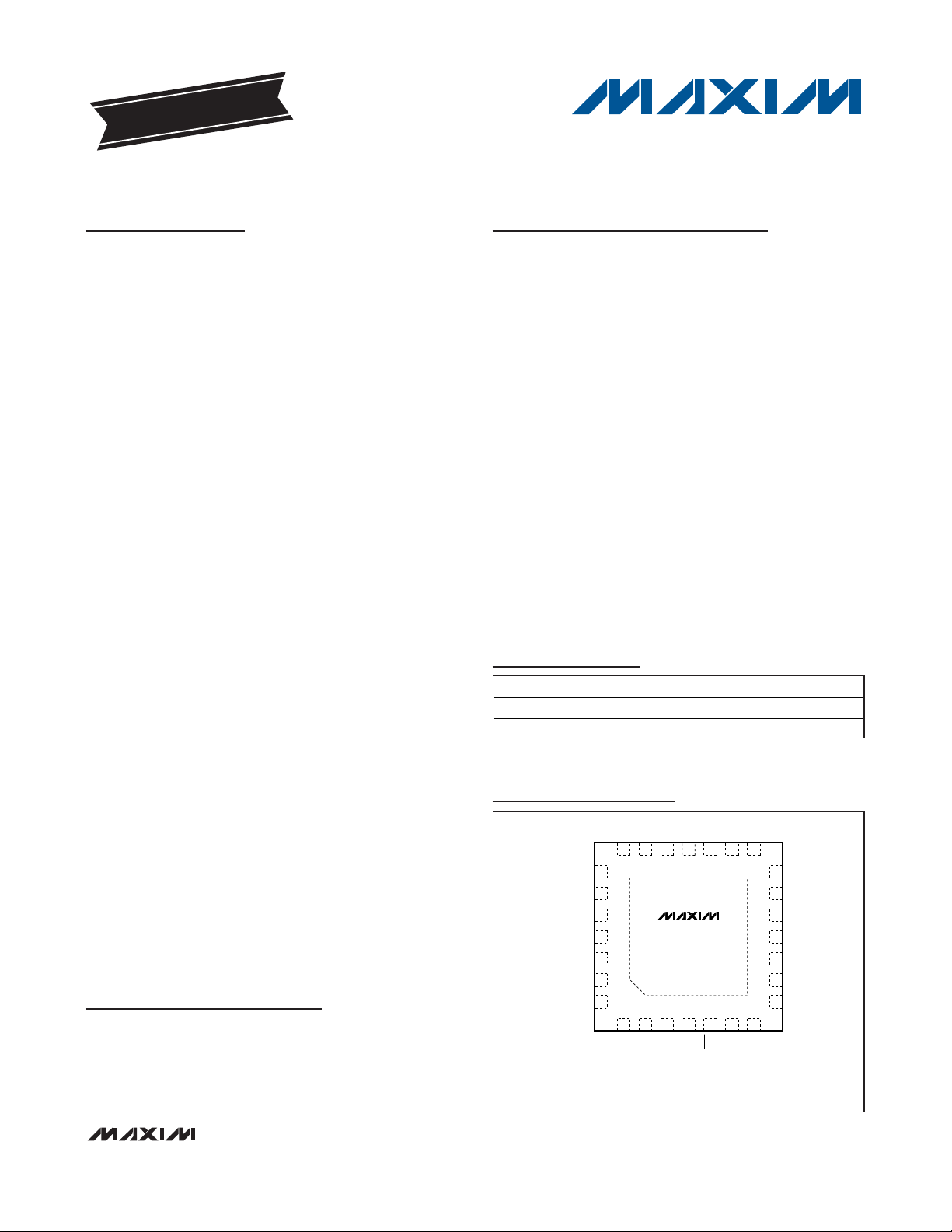
The MAX17007A/MAX17008 are available in a spacesaving, 28-pin, 4mm x 4mm, thin QFN package with an
exposed backside pad.
Applications
Features
o Dual Quick-PWM with Fast Transient Response
o Automatic Dynamic REFIN1 Detection and
PGOOD1/Fault Blanking
o Fixed and Adjustable Output Voltages
±0.7% Output Accuracy Over Line and Load
OUT1: 0 to 2V Dynamic Output or Preset 1.05V
OUT2: 0.7V to 2V Range or Preset 1.5V
o Resistor-Programmable Switching Frequency
o Integrated BST Switches
o Differential Current-Sense Inputs
Low-Cost DCR Sensing or Accurate CurrentSense Resistors
Internally Coupled Current-Sense Compensation
o Combinable Mode Supports High-Current
Dynamic Output Voltages
o Selectable Forced-PWM, Pulse Skip, or Ultrasonic
Mode Operation
o 26V Maximum Input Voltage Rating
o Independent Enable Inputs
o Independent Power-Good Outputs
o Overvoltage Protection (MAX17007A Only)
o Undervoltage/Thermal Protection
o Voltage Soft-Start and Soft-Shutdown
MAX17007A/MAX17008
Dual and Combinable QPWM Graphics
Core Controllers for Notebook Computers
________________________________________________________________
Maxim Integrated Products
1
MAX17007A
MAX17008
18
THIN QFN
(4mm x 4mm)
4175166
15
1422
7
19
3202
21
1323
1224
1125
1026
927
828
1
LX1
DH1
PGOOD1
EN1
CSH1
TOP VIEW
*EP
*EP = EXPOSED PAD.
CSL1
REFIN1
LX2
DH2
PGOOD2
EN2
CSH2
CSL2
FB2
BST2
PGND
DL2
VDDDL1
GND
BST1
REF
ILIM1
(CCI) ILIM2
V
CC
SKIP
TON1
TON2
+
Pin Configuration
Ordering Information
19-3200; Rev 2; 10/08
For pricing, delivery, and ordering information, please contact Maxim Direct at 1-888-629-4642,
or visit Maxim’s website at www.maxim-ic.com.
EVALUATION KIT
AVAILABLE
+
Denotes a lead-free/RoHS-compliant package.
*
EP = Exposed pad.
PART TEMP RANGE PIN-PACKAGE
MAX17007AGTI+ -40°C to +105°C 28 Thin QFN-EP*
MAX17008GTI+ -40°C to +105°C 28 Thin QFN-EP*
Notebook Computers
Low-Power I/O Supplies
GPU Core Supplies
2 to 4 Li+ Cells BatteryPowered Devices
Quick-PWM is a trademark of Maxim Integrated Products, Inc.
Page 2
MAX17007A/MAX17008
Dual and Combinable QPWM Graphics
Core Controllers for Notebook Computers
2 _______________________________________________________________________________________
ABSOLUTE MAXIMUM RATINGS
ELECTRICAL CHARACTERISTICS
(VIN= 12V, VDD= VCC= V
EN1
= V
EN2
= 5V, V
REFIN1
= 2V, SKIP = GND, TA= 0 to +85°C, unless otherwise noted. Typical values are
at T
A
= +25°C.)
Stresses beyond those listed under “Absolute Maximum Ratings” may cause permanent damage to the device. These are stress ratings only, and functional
operation of the device at these or any other conditions beyond those indicated in the operational sections of the specifications is not implied. Exposure to
absolute maximum rating conditions for extended periods may affect device reliability.
BST1, BST2 to GND ...............................................-0.3V to +34V
BST1, BST2 to V
DD
.................................................-0.3V to +28V
TON1, TON2 to GND..............................................-0.3V to +28V
V
DD
to GND..............................................................-0.3V to +6V
V
DD
to VCC............................................................-0.3V to +0.3V
LX1 to BST1..............................................................-6V to +0.3V
LX2 to BST2..............................................................-6V to +0.3V
DH1 to LX1 ..............................................-0.3V to (V
BST1
+ 0.3V)
DH2 to LX2 ..............................................-0.3V to (V
BST2
+ 0.3V)
ILIM1, ILIM2, REF to GND ..........................-0.3V to (V
CC
+ 0.3V)
CSH1, CSH2, CSL1, CSL2, FB2, REFIN1 to GND....-0.3V to +6V
EN1, EN2, SKIP, PGOOD1, PGOOD2 to GND.........-0.3V to +6V
DL1 to GND ................................................-0.3V to (V
DD
+ 0.3V)
DL2 to PGND..............................................-0.3V to (V
DD
+ 0.3V)
PGND to GND ......................................................-0.3V to + 0.3V
REF Short Circuit to GND ...........................................Continuous
Continuous Power Dissipation (T
A
= +70°C)
28-Pin TQFN T2844-1
(derate 20.8mW/°C above +70°C) ............................1667mW
Extended Operating Temperature Range .........-40°C to +105°C
Junction Temperature......................................................+150°C
Storage Temperature Range .............................-65°C to +150°C
Lead Temperature (soldering, 10s) .................................+300°C
PARAMETER SYMBOL CONDITIONS MIN TYP MAX UNITS
PWM CONTROLLER
Input Voltage Range V
IN
4.5 26 V
Quiescent Supply Current
(V
DD
, VCC)
I
DD
+ I
CC
Output forced above regulation vo ltage,
V
EN1
= V
EN2
= 5V
1.7 2.5 mA
Shutdown Supply Current
(V
DD
, VCC)
I
SHDN
EN1 = EN2 = GND, TA = +25°C 0.1 5 μA
R
TON1
= R
TON2
=
97.5k (600kHz)
142
(-15%)
174
194
(+15%)
R
TON1
= R
TON2
=
200k (300kHz)
305
(-10%)
336
368
(+10%)
On-Time (Note 1) t
ON1
, t
ON2
VIN = 12V,
V
CSL1
= V
CSL2
=
V
CCI
= 1.2V,
separate or
combined mode
R
TON1
= R
TON2
=
302.5 k (200kH z)
425
(-15%)
500
575
(+15%)
ns
Minimum Off-Time t
OFF(MIN)
(Note 1) 250 400 ns
TON1, TON2, Shutdown Supply
Current
I
TON1
,
I
TON2
EN1 = EN2 = GND, V
TON1
= V
TON2
= 26V,
V
DD
= 0 or 5V, TA = +25°C
0.01 1 μA
REFIN1 Voltage Range V
REFIN1
(Note 2) 0 V
REF
V
FB2 Regulation Voltage V
FB2
Adju stable mode 0.7 V
FB2 Input Voltage Range Preset mode 1.7 2.3 V
FB2 Combined-Mode Threshold Comb ined mode 3.8
V
CC
-
1V
VCC -
0.4
V
REFIN1 Dual Mode™
Switcho ver Threshold
3.8
VCC -
1V
VCC -
0.4
V
REFIN1, FB2 Bias Current
I
REFIN1
,
I
FB2
REFIN1 = 0.5V to 2V;
V
FB2
= 0.7V, TA = +25°C
-0.1 +0.1 μA
V
CSL1
Measured at CSL1, REFIN1 = VCC,
V
IN
= 2V to 26V, SKIP = VCC (Note 2)
1.043 1.05 1.057 V
TA = +25°C -12 +12
REFIN1 = 500mV,
SKIP = V
CC
TA = 0°C to +85°C -20 +20
SMPS1 Voltage Accuracy
V
CSL1
-
V
REFIN1
REFIN1 = 2V, SKIP = VCC -20 +20
mV
Dual Mode is a trademark of Maxim Integrated Products, Inc.
Page 3
MAX17007A/MAX17008
Dual and Combinable QPWM Graphics
Core Controllers for Notebook Computers
_______________________________________________________________________________________ 3
PARAMETER SYMBOL CONDITIONS MIN TYP MAX UNITS
SMPS2 Voltage Accuracy V
CSL2
Measured at CSL2, FB2 = REF,
V
IN
= 2V to 26V, SKIP = V
CC
1.489 1.5 1.511 V
Load Regulation Error I
LOAD
= 0 to full load, SKIP = V
CC
(Note 3) 0.1 %
Line Regulation Error VDD = 4.5V to 5.5V, VIN = 4.5V to 26V (Note 3) 0.25 %
CSL1 Soft-Start/-Stop Slew Rate SR
SS1
Risi ng/fall ing edge on EN1 1.25 mV/μs
FB2 Soft-Start/-Stop Slew Rate SR
SS2
Rising/falling edge on EN2 0.63 mV/μs
Dynamic REFIN1 Slew Rate SR
DYN
Risi ng edge on REFIN1 11.4 mV/μs
INTERNAL REFERENCE
Reference Voltage V
REF
VDD = 4.5V to 5.5V 1.990 2.000 2.010 V
Reference Lockout Voltage V
REF(UVLO)
Risi ng edge, hysteresis = 230mV 1.8 V
Reference Load Regulation I
REF
= -10μA to +100μA 1.980 2.015 mV
FAULT DETECTION
With respect to the internal target vo ltage
(error comparator threshold); rising edge;
hystere sis = 50mV
260 300 340 mV
Dynamic transition V
REF
+ 0.30 V
SMPS1 Overvoltage Trip
Threshold and PGOOD1 Upper
Threshold
(MAX17007A Only)
V
OVP1
,
V
PG1_H
Minimum OVP threshold 0.7 V
SMPS2 Adjustable Mode
Overvoltage Trip Threshold and
PGOOD2 Upper Threshold
(MAX17007A Only)
V
OVP2
,
V
PG2_H
With respect to the internal target vo ltage
0.7V (error comparator threshold);
hystere sis = 50mV
120 150 180 mV
Output Overvoltage Fault
Propagati on De lay
(MAX17007A Only)
t
OVP
CSL1/FB2 forced 25mV above trip threshold 5 μs
SMPS1 Undervoltage Protection
Trip Threshold and Lower
PGOOD1 Threshold
V
UVP1
,
V
PG1_L
With respect to the internal target vo ltage
(error comparator threshold); falling edge;
hystere sis = 50mV
-240 -200 -160 mV
SMPS2 Undervoltage Protection
Trip Threshold and Lower
PGOOD2 Threshold
V
UVP2
,
V
PG2_L
With respect to the internal target vo ltage
0.7V (error comparator threshold);
falling edge; hysteresis = 50mV
-130 -100 -70 mV
Output Undervoltage Fault
Propagati on De lay
t
UVP
CSL1/FB2 forced 25mV below trip threshold 90 205 360 μs
UVP falling edge, 25mV overdrive 5
OVP rising edge, 25mV overdrive 5
PGOOD_ Propagation Dela y t
PGOOD
Startup delay from regulation 90 205 360
μs
PGOOD_ Output Low Voltage I
SINK
= 3mA 0.4 V
PGOOD_ Lea kage Current I
PGOOD
CSL1 = REFIN1, FB2 = 0.7V (PGOOD_ high
impedance), PGOOD_ forced to 5V, T
A
= +25°C
1 μA
Dynamic REFIN1 Transition
Fault-Blanking Threshold
Fault blanking initiated; REFIN1 deviation
from the internal target vo ltage (error
comparator threshold); hy steresis = 10mV
±50 mV
Thermal-Shutdown Threshold T
SHDN
Hysteresis = 15°C (Note 3) 160 °C
VCC Undervoltage Lockout
Threshold
V
UVLO(VCC)
Ri sing edge, PWM disab led below this level,
hysteresis = 100mV
3.95 4.20 4.45 V
ELECTRICAL CHARACTERISTICS (continued)
(VIN= 12V, VDD= VCC= V
EN1
= V
EN2
= 5V, V
REFIN1
= 2V, SKIP = GND, TA= 0 to +85°C, unless otherwise noted. Typical values are
at T
A
= +25°C.)
Page 4
MAX17007A/MAX17008
Dual and Combinable QPWM Graphics
Core Controllers for Notebook Computers
4 _______________________________________________________________________________________
ELECTRICAL CHARACTERISTICS (continued)
(VIN= 12V, VDD= VCC= V
EN1
= V
EN2
= 5V, V
REFIN1
= 2V, SKIP = GND, TA= 0 to +85°C, unless otherwise noted. Typical values are
at T
A
= +25°C.)
PARAMETER SYMBOL CONDITIONS MIN TYP MAX UNITS
CURRENT LIMIT
CSH1, CSH2 0 2.3
Current-Sense Input Range
CSL1, CSL2 0 2.3
V
Current-Sense Input (CSH_)
Leakage Current
CSH_ = GND or V
CC
, TA = +25°C -0.2 +0.2 μA
Current-Sense Input (CSL_)
Leakage Current
CSL_= CSL_ = 2V, T
A
= +25°C 1 μA
TA = +25°C 28 30 32
V
CSH_
- V
CSL_
ILIM1 = ILIM2 = REF
T
A
= 0°C to +85°C 27 30 33
V
CSH_
- V
CSL_
, ILIM1 = ILIM2 = VCC 56 60 64
V
CSH_
- V
CSL_
, ILIM1 = ILIM2 = OPEN 42 45 48
Current-Limit Threshold (Fixed) V
CSLIMIT
V
CSH_
- V
CSL_,
ILIM1 = ILIM2 = GND 13 15 17
mV
Current-Limit Threshold
(Negative)
V
NEG
V
CSH_
- V
CSL_
, SKIP = V
CC
-1.2 x
V
CSLIMIT
mV
Current-Limit Threshold
(Zero Crossing)
V
ZX
V
CSH_
- V
CSL_
, SKIP = GND or OPEN;
ILIM1 = ILIM2 = REF
1 mV
Ultrasonic Frequency
SKIP = open (3.3V); V
CSL1
= V
REFIN1
+ 50mV;
V
CSL2
= V
FB2
+ 50mV
20 kHz
V
CSL1
= V
REF1
+ 50mV 22 33 46
Ultrasonic Current-Limit
Threshold
SKIP = open (3.3V)
V
CSL2
= V
FB2
+ 50mV 18 30 46
mV
Current-Balance Amplifier (GMI)
Offset
[V(CSH1,CSL1) - V(CSH2,CSL2)] at I
CCI
= 0 -3 +3 mV
Current-Balance Amplifier (GMI)
Transconductance
I
CCI
/[V(CSH1,CSL1) - V(CSH2,CSL2)];
V
CCI
= V
CSL1
= V
CSL2
= 0.5V to 2V, and
V(CSH_,CSL_) = -60.0mV to +60.0mV,
ILIM1 = GND
180 μS
GATE DRIVERS
Low state (pulldown) 1.7 4.0
DH1, DH2 Gate-Driver
On-Resistance
R
ON(DH)
BST_ - LX_ forced
to 5V
High state (pullup) 1.7 4.0
High state (pullup) 1.3 3.0
DL1, DL2 Gate-Driver
On-Resistance
R
ON(DL)
Low state (pulldown) 0.6 2.5
DH1, DH2 Gate-Driver
Source/Sink Current
I
DH
DH_ forced to 2.5V, BST_ - LX_ forced to
5V
1.2 A
DL1, DL2 Gate-Driver
Source Current
I
DL(S OURC E)
DL_ forced to 2.5V 1 A
DL1, DL2 Gate-Driver
Sink Current
I
DL(S INK)
DL_ forced to 2.5V 2.4 A
DH_ low to DL high 10 25 40
Driver Propagation Delay
DL_ low to DH high 15 30 45
ns
Page 5
MAX17007A/MAX17008
Dual and Combinable QPWM Graphics
Core Controllers for Notebook Computers
_______________________________________________________________________________________ 5
ELECTRICAL CHARACTERISTICS (continued)
(VIN= 12V, VDD= VCC= V
EN1
= V
EN2
= 5V, V
REFIN1
= 2V, SKIP = GND, TA= 0 to +85°C, unless otherwise noted. Typical values are
at T
A
= +25°C.)
PARAMETER SYMBOL CONDITIONS MIN TYP MAX UNITS
DL_ fall ing, CDL = 3nF 10 20
DL_ Transition Time
DL_ rising, C
DL
= 3nF 10 20
ns
DH_ falling, CDH = 3nF 10 20
DH_ Transition Time
DH_ ri sing, C
DH
= 3nF 10 20
ns
Internal BST_ Switch
On-Resistance
R
BST_ IBST_
= 10mA, VDD = 5V 6.5 11.0
INPUTS AND OUTPUTS
EN1, EN2 Logic-Input Threshold
EN1, EN2 ris ing edge,
hysteresis = 300mV/600mV (min/max)
1.20 1.70 2.20 V
Logic-Input Current EN1, EN2, TA = +25°C -0.5 +0.5 μA
High (5V)
V
CC
-
0.3
Open (3.3V) 3.0 3.6
Ref (2.0V) 1.7 2.3
Quad-Level Input-Logic Leve ls SKIP, ILIM1, ILIM2
Low (GND) 0.4
V
Quad-Level Logic-Input Current
SKIP, ILIM1, ILIM2 forced to GND or V
CC
,
T
A
= +25°C
-2 +2 μA
ELECTRICAL CHARACTERISTICS
(VIN= 12V, VDD= VCC= V
EN1
= V
EN2
= 5V, V
REFIN1
= 2V, SKIP = GND, TA= -40°C to +105°C, unless otherwise noted.) (Note 4)
PARAMETER SYMBOL CONDITIONS MIN MAX UNITS
PWM CONTROLLER
Input Voltage Range V
IN
4.5 26 V
Quiescent Supply Current
(V
DD
, VCC)
I
DD
+ I
CC
Output forced above regulation vo ltage,
V
EN1
= V
EN2
= 5V
2.5 mA
R
TON1
= R
TON2
=
97.5k (600 kHz)
142 194
R
TON1
= R
TON2
=
200k (300kHz)
305 368
On-Time (Note 1)
t
ON1
,
t
ON2
VIN = 12V,
V
CSL1
= V
CSL2
=
V
CCI
= 1.2V,
separate or
combined mode
R
TON1
= R
TON2
=
302.5 k (200kH z)
425 575
ns
Minimum Off-Time t
OFF(MIN)
(Note 1) 400 ns
REFIN1 Voltage Range V
REFIN1
0 V
REF
V
FB2 Input Voltage Range Preset mode 1.7 2.3 V
FB2 Combined-Mode Threshold Comb ined mode 3.75
V
CC
-
0.4
V
REFIN1, FB2 Bias Current
I
REFIN1
,
I
FB2
-0.1 +0.1 μA
Page 6
MAX17007A/MAX17008
Dual and Combinable QPWM Graphics
Core Controllers for Notebook Computers
6 _______________________________________________________________________________________
ELECTRICAL CHARACTERISTICS (continued)
(VIN= 12V, VDD= VCC= V
EN1
= V
EN2
= 5V, V
REFIN1
= 2V, SKIP = GND, TA= -40°C to +105°C, unless otherwise noted.) (Note 4)
PARAMETER SYMBOL CONDITIONS MIN MAX UNITS
REFIN1 Dual-Mode
Switcho ver Threshold
3.75
VCC -
0.4
V
SMPS1 Voltage Accuracy V
CSL1
Measured at CSL1, REFIN1 = V
CC;
VIN = 2V to 26V, SKIP = V
CC
(Note 2)
1.039 1.061 V
SMPS2 Voltage Accuracy V
CSL2
Measured at CSL2, FB2 = REF;
V
IN
= 2V to 26V, SKIP = V
CC
(Note 2)
1.485 1.515 V
INTERNAL REFERENCE
Reference Voltage V
REF
VDD = 4.5V to 5.5V 1.985 2.015 V
FAULT DETECTION
SMPS1 Overvoltage Trip
Threshold and PGOOD1
Upper Threshold
(MAX17007A Only)
V
OVP1
,
V
PG1_H
With respect to the internal target vo ltage
(error comparator threshold); rising edge;
hystere sis = 50mV
260 340 mV
SMPS2 Overvoltage Trip
Threshold and PGOOD2
Upper Threshold
(MAX17007A Only)
V
OVP2
,
V
PG2_H
With respect to the internal target vo ltage
0.7V (error comparator threshold);
hystere sis = 50mV
120 180 mV
SMPS1 Undervoltage Protection
Trip Threshold and Lower
PGOOD1 Threshold
V
UVP1
,
V
PG1_L
With respect to the internal target vo ltage
(error comparator threshold) falling edge;
hystere sis = 50mV
-240 -160 mV
SMPS2 Undervoltage Protection
Trip Threshold and Lower
PGOOD2 Threshold
V
UVP2
,
V
PG2_L
With respect to the internal target vo ltage
0.7V (error comparator threshold)
falling edge; hysteresis = 50mV
-130 -70 mV
Output Undervoltage Fault
Propagati on De lay
t
UVP
REFIN1/FB2 forced 25mV below trip
threshold
90 360 μs
PGOOD_ Propagation Dela y t
PGOOD
Startup delay from regulation 90 360 μs
PGOOD_ Output Low Voltage I
SINK
= 3mA 0.4 V
VCC Undervoltage Lockout
Threshold
V
UVLO(VCC)
Ri sing edge, PWM disab led below this level;
hysteresis = 100mV
3.8 4.45 V
CURRENT LIMIT
CSH1, CSH2 0 2.3
Current-Sense Input Range
CSL1, CSL2 0 2.3
V
Current-Limit Threshold (Fixed) V
CSLIMIT VCSH_
- V
CSL_
, ILIM1 = ILIM2 = REF 27 33 mV
Ultrasonic Frequency
SKIP = OPEN (3.3V);
V
CSL1
= V
REFIN1
+ 50mV;
V
CSL2
= V
FB2
+ 50mV
18 kHz
V
CSL1
= V
REF1
+ 50mV 22 46
Ultrasonic Current-Limit
Threshold
SKIP = OPEN (3.3V)
V
CSL2
= V
FB2
+ 50mV 18 46
mV
Current-Balance Amplifier (GMI)
Offset
[V(CSH1,CSL1) - V(CSH2,CSL2)] at I
CCI
= 0 -3 +3 mV
Page 7
MAX17007A/MAX17008
Dual and Combinable QPWM Graphics
Core Controllers for Notebook Computers
_______________________________________________________________________________________ 7
Note 1: On-time and off-time specifications are measured from 50% point to 50% point at the DH pin with LX = GND, V
BST
= 5V, and
a 250pF capacitor connected from DH to LX. Actual in-circuit times might differ due to MOSFET switching speeds.
Note 2: The 0 to 0.5V range is guaranteed by design, not production tested.
Note 3: Not production tested.
Note 4: Specifications at T
A
= -40°C to +105°C are guaranteed by design, not production tested.
ELECTRICAL CHARACTERISTICS (continued)
(VIN= 12V, VDD= VCC= V
EN1
= V
EN2
= 5V, V
REFIN1
= 2V, SKIP = GND, TA= -40°C to +105°C, unless otherwise noted.) (Note 4)
PARAMETER SYMBOL CONDITIONS MIN MAX UNITS
GATE DRIVERS
Low state (pulldown) 4.5
DH1, DH2 Gate-Driver
On-Resistance
R
ON(DH)
BST_ - LX_ forced to
5V
High state (pullup) 4.0
High state (pullup) 3
DL1, DL2 Gate-Driver
On-Resistance
R
ON(DL)
Low state (pulldown) 2.5
DH_ low to DL high 8 42
Driver Propagation Delay
DL_ low to DH high 12 48
ns
Internal BST_ Switch
On-Resistance
R
BST_ IBST_
= 10mA, VDD = 5V 12
INPUTS AND OUTPUTS
EN1, EN2 Logic-Input Threshold
EN1, EN2 ris ing edge;
hysteresis = 300mV/600mV (min/max)
1.20 2.20 V
High (5V)
V
CC
-
0.3
Open (3.3V) 3.0 3.6
Ref (2.0V) 1.7 2.3
Quad-Level Input Logic Levels SKIP, ILIM1, ILIM2
Low (GND) 0.4
V
Page 8
MAX17007A/MAX17008
Dual and Combinable QPWM Graphics
Core Controllers for Notebook Computers
8 _______________________________________________________________________________________
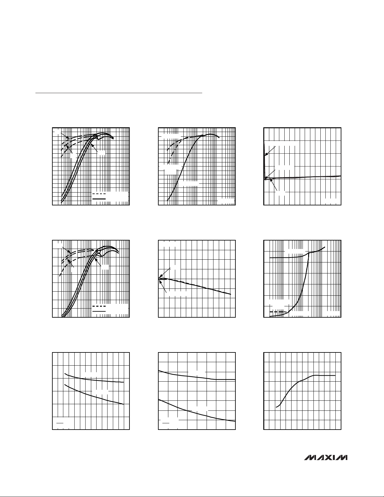
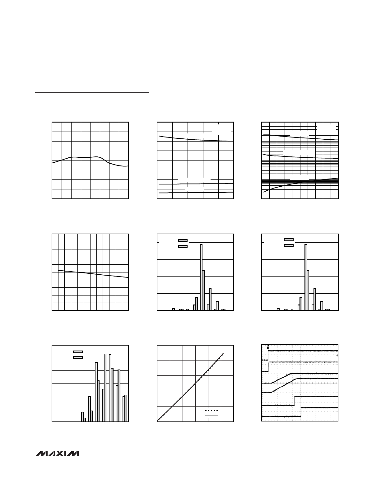
Typical Operating Characteristics
(Circuit of Figure 1, VIN= 12V, VDD= 5V, SKIP = GND, TA= +25°C, unless otherwise noted.)
SMPS2 1.5V EFFICIENCY
vs. LOAD CURRENT
MAX17007A/8 toc01
LOAD CURRENT (A)
EFFICIENCY (%)
1010.1
50
60
70
80
90
100
40
20
30
10
0.01 100
6V
12V
20V
SKIP MODE
PWM MODE
SMPS2 1.5V EFFICIENCY
vs. LOAD CURRENT
MAX17007A/8 toc02
LOAD CURRENT (A)
EFFICIENCY (%)
1010.1
50
60
70
80
90
100
40
20
30
10
0.01 100
SKIP MODE
PWM MODE
VIN = 12V
ULTRASONIC
MODE
SMPS2 1.5V OUTPUT VOLTAGE
vs. LOAD CURRENT
MAX17007A/8 toc03
LOAD CURRENT (A)
OUTPUT VOLTAGE (V)
105
1.50
1.52
1.54
1.48
015
SKIP MODE
ULTRASONIC MODE
PWM
VIN = 12V
COMBINED 1.2V EFFICIENCY
vs. LOAD CURRENT
MAX17007A/8 toc04
LOAD CURRENT (A)
EFFICIENCY (%)
1010.1
50
60
70
80
90
100
40
20
30
10
0.01 100
SKIP MODE
PWM MODE
6V
12V
20V
COMBINED 1.2V OUTPUT VOLTAGE
vs. LOAD CURRENT
MAX17007A/8 toc05
LOAD CURRENT (A)
OUTPUT VOLTAGE (V)
16 20842412
1.19
1.20
1.21
1.22
1.18
028
SKIP MODE
PWM
VIN = 12V
SMPS2 SWITCHING FREQUENCY
vs. LOAD CURRENT
MAX17007A/8 toc06
LOAD CURRENT (A)
SWITCHING FREQUENCY (kHz)
1010.1
200
250
300
350
150
50
100
0
0.01 100
SKIP MODE
PWM MODE
VIN = 12V
ULTRASONIC
MODE
SMPS2 SWITCHING FREQUENCY
vs. INPUT VOLTAGE
MAX17007A/8 toc07
INPUT VOLTAGE (V)
SWITCHING FREQUENCY (kHz)
20424
250
300
350
200
02881216
VIN = 12V
SKIP = 5V
I
OUT2
= 5A
I
OUT2
= 0A
SMPS2 SWITCHING FREQUENCY
vs. TEMPERATURE
MAX17007A/8 toc08
TEMPERATURE (°C)
SWITCHING FREQUENCY (kHz)
040-20 60
290
270
310
330
250
-40 1201008020
VIN = 12V
SKIP = 5V
I
OUT2
= 5A
I
OUT2
= 0A
SMPS2 MAXIMUM OUTPUT CURRENT
vs. INPUT VOLTAGE
MAX17007A/8 toc09
INPUT VOLTAGE (V)
MAXIMUM OUTPUT CURRENT (A)
20424
12
11
13
14
10
02881216
Page 9
MAX17007A/MAX17008
Dual and Combinable QPWM Graphics
Core Controllers for Notebook Computers
_______________________________________________________________________________________ 9
SMPS2 MAXIMUM OUTPUT CURRENT
vs. TEMPERATURE
MAX17007A/8 toc10
TEMPERATURE (°C)
MAXIMUM OUTPUT CURRENT (A)
80400
11
12
13
14
10
-40 1206020-20 100
VIN = 12V
NO-LOAD SUPPLY CURRENT
vs. INPUT VOLTAGE
MAX17007A/8 toc11
INPUT VOLTAGE (V)
SUPPLY CURRERT (I
BIAS
) (mA)
2016
4
8
12
16
0
6
10
14
2
424812
SKIP MODE
PWM MODE
ULTRASONIC MODE
EN1 = HIGH
EN2 = LOW
NO-LOAD INPUT CURRENT
vs. INPUT VOLTAGE
MAX17007A/8 toc12
INPUT VOLTAGE (V)
INPUT CURRENT (mA)
2016
0.1
1
10
100
0.01
424812 1814 22610
SKIP MODE
PWM MODE
ULTRASONIC MODE
EN1 = HIGH
EN2 = LOW
REFERENCE VOLTAGE
vs. REFERENCE LOAD CURRENT
MAX17007A/8 toc13
REFERENCE LOAD CURRENT (μA)
REFERENCE VOLTAGE (V)
8060
1.99
1.97
2.01
2.03
2.05
1.95
-20 10020 400
REFIN1 TO CSL1 OFFSET VOLTAGE
DISTRIBUTION
MAX17007A/8 toc14
OFFSET VOLTAGE (mV)
SAMPLE PERCENTAGE (%)
3.0
60
50
70
80
20
10
30
40
90
0
-5.0 5.0-1.0 1.0-3.0
SAMPLE SIZE = 100
TA = +85°C
T
A
= +25°C
SMPS1 PRESET 1.05V
VOLTAGE DISTRIBUTION
MAX17007A/8 toc15
SMPS1 VOLTAGE (mV)
SAMPLE PERCENTAGE (%)
1.053
60
50
70
80
20
10
30
40
90
0
1.045 1.0551.049 1.0511.047
SAMPLE SIZE = 100
TA = +85°C
T
A
= +25°C
SMPS2 PRESET 1.5V
VOLTAGE DISTRIBUTION
MAX17007A/8 toc16
SMPS2 VOLTAGE (mV)
SAMPLE PERCENTAGE (%)
1.503
15
10
20
25
5
30
0
1.495 1.5051.499 1.5011.497
SAMPLE SIZE = 100
TA = +85°C
T
A
= +25°C
COMBINED-MODE CURRENT BALANCE
vs. LOAD CURRENT
MAX17007A/8 toc17
LOAD CURRENT (A)
V
CSH -
V
CSL
(mV)
201552510
50
40
20
10
30
0
030
SMPS1
SMPS2
SOFT-START WAVEFORM
MAX17007A/8 toc18
400μs/div
A
B
E
F
C
D
5V
A. EN1, EN2, 5V/div
B. REF, 2V/div
C. V
OUT1
, 1V/div
D. V
OUT2
, 1V/div
E. PGOOD1, 5V/div
F. PGOOD2, 5V/div
0
2V
0
5V
0
0
5V
0
1.05V
1.5V
0
Typical Operating Characteristics (continued)
(Circuit of Figure 1, VIN= 12V, VDD= 5V, SKIP = GND, TA= +25°C, unless otherwise noted.)
Page 10
MAX17007A/MAX17008
Dual and Combinable QPWM Graphics
Core Controllers for Notebook Computers
10 ______________________________________________________________________________________
Typical Operating Characteristics (continued)
(Circuit of Figure 1, VIN= 12V, VDD= 5V, SKIP = GND, TA= +25°C, unless otherwise noted.)
SMPS1 STARTUP WAVEFORM
(HEAVY LOAD)
MAX17007A/8 toc19
200μs/div
A
B
E
F
G
C
D
5V
A. EN1, 5V/div
B. REF, 2V/div
C. V
OUT1
, 500mV/div
D. I
LX1
, 10A/div
E. PGOOD1, 10V/div
F. LX1, 10V/div
G. DL1, 10V/div
0
2V
5V
0
12V
0
5V
0
0
1.05V
0
8A
I
OUT1
= 8A
SMPS1 STARTUP WAVEFORM
(LIGHT LOAD)
MAX17007A/8 toc20
200μs/div
A
B
E
F
G
C
D
5V
A. EN1, 5V/div
B. REF, 2V/div
C. V
OUT1
, 500mV/div
D. I
LX1
, 5A/div
SKIP = 5V
I
OUT1
= 2A
E. PGOOD1, 10V/div
F. LX1, 10V/div
G. DL1, 10V/div
0
2V
0
1.05V
0
2A
0
5V
0
5V
0
0
12V
SMPS1 SHUTDOWN WAVEFORM
MAX17007A/8 toc21
200μs/div
A
B
E
F
G
C
D
5V
A. EN1, 5V/div
B. REF, 5V/div
C. V
OUT1
, 500mV/div
D. I
LX1
, 5A/div
E. PGOOD1, 10V/div
F. LX1, 10V/div
G. DL1, 10V/div
I
OUT1
= 0.5A
SKIP = GND
0
2V
1.05V
0
0
0
5V
0
5V
0
12V
SMPS2 LOAD-TRANSIENT RESPONSE
(PWM MODE)
MAX17007A/8 toc22
20μs/div
A
B
C
A. V
OUT2
, 50mV/div
B. I
LX2
, 10A/div
C. LX2, 10V/div
1.5V
10A
2A
12V
0
I
OUT2
= 2A TO 10A TO 2A
SKIP = 5V
SMPS2 LOAD-TRANSIENT RESPONSE
(SKIP MODE)
MAX17007A/8 toc23
20μs/div
A
B
C
A. V
OUT2
, 50mV/div
B. I
LX2
, 10A/div
C. LX2, 10V/div
1.5V
8A
0A
12V
0
I
OUT2
= 0.5A TO 8.5A TO 0.5A
SKIP = GND
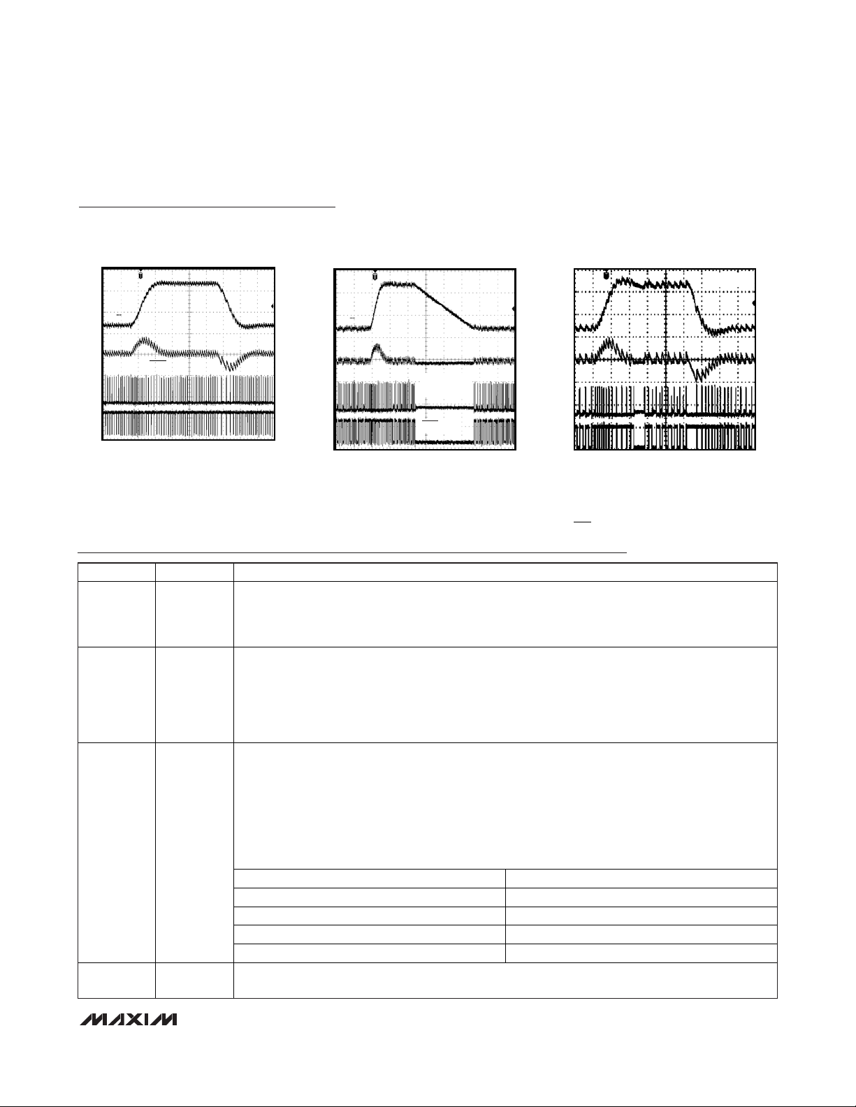
SMPS1 OUTPUT OVERLOAD WAVEFORM
MAX17007A/8 toc24
200μs/div
A
B
E
C
D
I
OUT1
= 2A TO 15A
A. V
OUT1
, 500mV/div
B. I
LX1
, 10A/div
C. LX1, 10V/div
1.05V
10A
2A
5V
0
5V
12V
0
0
D. PGOOD1, 5V/div
E. DL1, 5V/div
SMPS1 OUTPUT OVERVOLTAGE
WAVEFORM
MAX17007A/8 toc25
40μs/div
A
B
C
A. V
OUT1
, 1V/div
B. PGOOD1, 5V/div
C. DL1, 5V/div
1.05V
0
5V
0
5V
0
Page 11
MAX17007A/MAX17008
Dual and Combinable QPWM Graphics
Core Controllers for Notebook Computers
______________________________________________________________________________________ 11
DYNAMIC OUTPUT VOLTAGE
TRANSITION (PWM MODE)
MAX17007A/8 toc26
20μs/div
A
B
C
D
I
OUT1
= 2A
REFIN1 = 1V
TO 1.2V TO 1V
1.2V
1V
0
2A
12V
0
5V
A. V
OUT1
, 100mV/div
B. I
LX1
, 10A/div
C. LX1, 10V/div
D. DL1, 5V/div
SKIP = 5V
DYNAMIC OUTPUT VOLTAGE
TRANSITION (SKIP MODE)
MAX17007A/8 toc27
40μs/div
A
B
C
D
I
OUT1
= 1A
1.2V
1V
0
0
12V
0
5V
A. V
OUT1
, 100mV/div
B. I
LX1
, 10A/div
C. LX1, 10V/div
D. DL1, 5V/div
REFIN1 = 1V
TO 1.2V TO 1V
SKIP = GND
DYNAMIC OUTPUT-VOLTAGE TRANSITION
(SKIP MODE-FORCED TRANSITION)
MAX17007A/8 toc28
20μs/div
A
B
C
D
1.2V
1V
0
0
12V
0
5V
A. V
OUT1
, 100mV/div
B. I
LX2
, 10A/div
I
OUT1
= 1A
REFIN1 = 1V TO 1.2V TO 1V
SKIP = REF
C. LX1, 10V/div
D. DL1, 5V/div
I
OUT1
= 3A
Pin Description
Typical Operating Characteristics (continued)
(Circuit of Figure 1, VIN= 12V, VDD= 5V, SKIP = GND, TA= +25°C, unless otherwise noted.)
PIN NAME FUNCTION
1 REF
2V Reference Voltage Output. B ypass REF to GND with a 2.2nF ceramic capac itor. The reference
can source up to 100μA. Load ing REF degrades output-voltage accuracy according to the REF
load regulation error (see theTypical Operating Characteristics). The reference shuts down when
both EN1 and EN2 are low.
2 ILIM1
Thi s four-level input determines the CSH1 to CSL1 current li mit for SMPS1:
V
CC
(5V) = 60mV current lim it
Open (3.3V) = 45mV current limit
REF (2V) = 30mV current limit
GND = 15mV current limit
In combined mode, ILIM1 sets the current-limit threshold for both sides.
Thi s four-level input determines the CSH2 to CSL2 current li mit for SMPS2:
V
CC
(5V) = 60mV current lim it
Open (3.3V) = 45mV current limit
REF (2V) = 30mV current limit
GND = 15mV current limit
In combined mode, ILIM2 is the current balance integrator (CCI) output pin. Connect a capacitor
(C
CCI
) between CCI and the output. The CCI capacitor va lue depends on the ILIM1 setting based
on the following table:
ILIM1 C
CCI
at ILIM2 (pF)
VCC (5V) 120
Open (3.3V) 180
REF (2V) 220
3
ILIM2
(CCI)
GND 470
4 V
CC
5V Analog Supply Input. Bypass VCC from VDD using a 10 resistor, and to analog ground us ing a
1μF ceramic capacitor.
Page 12

MAX17007A/MAX17008
Dual and Combinable QPWM Graphics
Core Controllers for Notebook Computers
12 ______________________________________________________________________________________
Pin Description (continued)
PIN NAME FUNCTION
5 SKIP
Pulse-Skipp ing Control Input. This four-level input determine s the mode of operation under normal
steady-state condition s and dynamic output-voltage transition s:
V
DD
(5V) = Forced-PWM operation
Open (3.3V) = Ultrasonic mode (without forced-PWM during transitions)
REF (2V) = Pulse-skipping mode (with forced-PWM during transitions)
GND = Pulse-sk ipping mode (without forced-PWM during transitions)
There are no dynamic transitions for SMPS2, so SKIP = 2V and SKIP = GND have the same pulse-
sk ipping behav ior for SMPS2 without an y forced-PWM transitions.
In combined mode, the ultrasonic mode is disabled, and the SKIP = open (3.3V) setting is ident ical
to the SKIP = GND setting.
6 TON1
Frequency-Setting Input for SMPS1. An e xternal resi stor between the input power source and TON1
sets the switching period (T
SW1
) of SMPS1:
T
SW1
= C
TON
(R
TON1
+ 6.5 k)
where C
TON
= 16.26pF.
TON1 is high impedance in shutdown.
In combined mode, TON1 sets the switching period for both SMPS1 and SMPS2.
7 TON2
Frequency-Setting Input for SMPS2. An e xternal resi stor between the input power source and TON2
sets the switching period (T
SW2
) of SMPS2:
T
SW2
= C
TON
(R
TON2
+ 6.5 k)
where C
TON
= 16.26pF.
Set TON2 to a switching frequency different from TON1. A 10% to 30% difference in switching
frequency between SMPS1 and SMPS2 is recommended.
TON2 is high impedance in shutdown.
In combined mode, TON2 may be left open.
8 REFIN1
External Reference Input for SMPS1. REFIN1 sets the feedback regulat ion voltage of CSL1. SMPS1
inc lude s an internal window comparator to detect REFIN1 vo ltage changes that are greater than
±50mV (typ), allowing the controller to blank PGOOD1 and the fault protectio n, and force the output
transition, if enabled. When REFIN1 i s tied to V
CC
, SMPS1 regulate s the output to 1.05V.
In combined mode, REFIN1 sets the feedback regulation voltage of the combined output.
9 CSL1
Output-Sense and Negative Current-Sense Input for SMPS1. When us ing the internal preset 1.05V
feedback d iv ider (REFIN1 = V
CC
), the controller uses CSL1 to sense the output voltage. Connect to
the negativ e terminal of the current-sense element. Figure 14 describes two different currentsensing options—using accurate sense resistors or lossless inductor DCR sensing.
10 CSH1
Positive Current-Sense Input for SMPS1. Connect to the positive termina l of the current-sense
element. Figure 14 describes two different current-sensing options—using accurate sense
resistors or lossless inductor DCR sensing.
11 EN1
Enable Control Input for SMPS1. Connect to V
CC
for normal operation. Pull EN1 low to disable
SMPS1. The controller s low ly ramps down the output voltage to ground and after the target voltage
reaches 0.1V, the controller forces DL1 low. When both EN1 and EN2 are low, the device enters the
low-power shutdown state.
In combined mode, EN1 controls the combined SMPS output. EN2 is unused and must be grounded.
12 PGOOD1
Open-Drain Power-Good Output for SMPS1. PGOOD1 is low when the SMPS1 voltage is more than 200mV
below or 300mV above the target voltage, during soft-start, and in shutdown. After the SMPS1 soft-start
circuit has terminated, PGOOD1 becomes high impedance 200μs after the output is in regulation.
PGOOD1 is blanked (forced high-impedance state) when a dynamic REFIN1 transition is detected.
13 DH1 High-Side Gate-Driver Output for SMPS1. DH1 swings from LX1 to BST1. DH1 is low in shutdown.
Page 13

MAX17007A/MAX17008
Dual and Combinable QPWM Graphics
Core Controllers for Notebook Computers
______________________________________________________________________________________ 13
Pin Description (continued)
PIN NAME FUNCTION
14 LX1
Inductor Connection for SMPS1. Connect LX1 to the switched side of the inductor. LX1 serve s a s the
lower supply rai l for the DH1 high-side gate driver.
15 BST1
Bootstrap Capacitor Connection for SMPS1. The MAX17007A/MAX17008 include an internal boost
switch/diode connected between V
DD
and BST1. Connect to an external capacitor as shown in Figure 1.
16 GND Ground. Analog and power ground connection for the low-side gate driver of SMPS1.
17 DL1
Low-Side Gate Driver Output for SMPS1. DL1 swing s from GND to V
DD
. DL1 is forced low after the shutdown
sequence has completed. DL1 is also forced high when an output overvoltage fault is detected, overriding
any negative current-limit condition that may be present. DL1 is forced low in V
CC
UVLO.
18 V
DD
5V Driver Supply Input. Connect VDD to VCC through a 10 resistor. Bypass to ground through a 2.2μF or
greater ceramic capacitor. V
DD
is internally connected to the BST diodes and the low-side gate drivers.
19 DL2
Low-Side Gate-Driver Output for SMPS2. DL2 swings from PGND to V
DD
. DL2 is forced low after the
shutdown sequence has completed. DL2 is also forced high when an output o vervoltage fault is
detected, overriding any negative current-limit condition that may be present. DL2 is forced low in V
CC
UVLO.
20 PGND Power Ground for the Low-Side Gate Driver of SMPS2
21 BST2
Bootstrap Capacitor Connection for SMPS2. The MAX17007A/MAX17008 include an internal boost switch/
diode connected between V
DD
and BST2. Connect to an external capacitor as shown in Figure 1.
22 LX2
Inductor Connection for SMPS2. Connect LX2 to the switched side of the inductor. LX2 serve s a s the
lower supply rai l for the DH2 high-side gate driver.
23 DH2 High-Side Gate-Driver Output for SMPS2. DH2 swings from LX2 to BST2. DH2 i s low in shutdown.
24 PGOOD2
Open-Drain Power-Good Output for SMPS2. PGOOD2 is low when the FB2 voltage is more than 100mV
below or 150mV above the target vo ltage, during soft-start, and in shutdown. After the SMPS2 soft-start
circuit has terminated, PGOOD2 becomes high impedance 200μs after the output is in regulation.
In combined mode, PGOOD2 is not used and can be left open.
25 EN2
SMPS2 Enable Input. Connect to V
CC
for normal operation. Pull EN2 low to d isable SMPS2. The
controller slowl y ramps down the output voltage to ground, and after the target vo ltage reache s 0.1V,
the controller force s DL2 low. When both EN1 and EN2 are low, the dev ice enters the low-power
shutdown state.
In combined mode, EN2 is not used and should be connected to GND.
26 CSH2
Positive Current-Sense Input for SMPS2. Connect to the positive terminal of the current-sense element.
Figure 14 describes two different current-sensing options—us ing accurate sense res istors or lossless
inductor DCR sensing.
27 CSL2
Output-Sense and Negative Current-Sense Input for SMPS2. When us ing the internal preset 1.5V
feedback divider (FB2 = REF), the controller uses CSL2 to sense the output voltage. Connect to the
negative terminal of the current-sense element. F igure 14 describes two different current-sens ing
options—using accurate sense resistors or lossless inductor DCR sensing.
28 FB2
SMPS2 Feedback Input. Adjust the SMPS2 voltage with a resistive voltage-divider between SMPS2
output and GND. Connect FB2 to REF for preset 1.5V output. Tie FB2 to V
CC
to conf igure the
MAX17007A/MAX17008 for combined-mode operation.
— EP Exposed Backside Pad. Connect to analog ground.
Page 14

MAX17007A/MAX17008
Dual and Combinable QPWM Graphics
Core Controllers for Notebook Computers
14 ______________________________________________________________________________________
MAX17007A
MAX17008
6
TON1
AGND
R
REFIN1
R
REFIN2
16
C
VCC
1μF
R2
100kΩ
TO SYSTEM
POWER-GOOD
R9
10Ω
R
TON1
220kΩ
R
NTC1
10kΩ
R4
3.01kΩ
R
TON2
180kΩ
C
REF
2.2nF
R
REFIN3
GND
PWR
PWR
PWR
AGND
PWR
AGND
2
ILIM1
3
ILIM2
(CCI)
5
SKIP
11
EN1
25
EN2
1
REF
R
REFIN1
= 80.6kΩ
R
REFIN2
= 121kΩ
R
REFIN3
= 249kΩ
8
REFIN1
12
PGOOD1
24
PGOOD2
7
TON2
15
BST1
13
DH1
14
LX1
17
DL1
N
H1
N
L1
20
PGND
10
CSH1
9
CSL1
28
FB2
4
V
CC
18
V
DD
REF
REF
+3.3V
H = 1.0V
L = 1.2V
4-LEVEL SKIP PIN
REF
+5V
CONNECT TO REF FOR
FIXED 1.5V OUTPUT
*LOWER INPUT VOLTAGES REQUIRE
ADDITIONAL INPUT CAPACITANCE.
V
IN
7V TO 20V
EP
POWER GROUND
ANALOG GROUND
R1
100kΩ
C
VDD
2.2μF
C1
0.22μF
C
BST1
0.1μF
PWR
D
L1
C
IN1
R3
1.5kΩ
C
OUT1
2 x 330μF
12mΩ
L1
1μH, 16A, 3mΩ
V
OUT1
1.2V/1.0V, 12A
ILIM1
ILIM2
V
CC
OPEN
REF
GND
R7
10Ω
C2
1nF
PWR
C
OUT1-CER
5 x 10μF
CERAMIC
V
OUT2
1.5V, 12A
R
NTC2
10kΩ
R6
3.01kΩ
PWR
AGND
PWR
21
BST2
23
DH2
22
LX2
19
DL2
N
H2
N
L2
26
CSH2
27
CSL2
V
IN
7V TO 20V
C3
0.22μF
C
BST2
0.1μF
PWR
D
L2
C
IN2
R5
1.5kΩ
C
OUT2
2 x 330μF
12mΩ
L2
1μH, 16A, 3mΩ
R8
10Ω
C4
1nF
PWR
C
OUT2-CER
5 x 10μF
CERAMIC
CURRENT
LIMIT
60mV
45mV
30mV
15mV
Figure 1. MAX17007A/MAX17008 Separate-Mode Standard Application Circuit
Page 15

MAX17007A/MAX17008
Dual and Combinable QPWM Graphics
Core Controllers for Notebook Computers
______________________________________________________________________________________ 15
V
OUT1
= 1.0V/1.2V AT 12A
(FIGURE 1)
V
OUT
= 1.5V AT 12A
(FIGURE 1)
COMPONENT
V
IN
= 7V to 20V
TON1 = 2 20 k (270 kHz)
VIN = 7V to 20V
TON2 = 1 80 k (330 kHz)
Input Capacitor
(per Pha se)
(2x) 10μF, 25V
Taiyo Yuden TMK432BJ106KM
(2x) 10μF, 25V
Taiyo Yuden TMK432BJ106KM
Output Capac itor
(2x) 330μF, 2.5V, 12m, C case
SANYO 2R5TPE330MCC2
(2x) 330μF, 2.5V, 12m, C case
SANYO 2R5TPE330MCC2
Inductor
1μH, 3.25m, 16A
Würth Electronics 7443552100
1μH, 3.25m, 16A
Würth Electronics 7443552100
Schottky Diode
2A, 30V Schottky diode (SMA)
Nihon EC21QS03L
Central Semiconductor
CMSH2-40M
2A, 30V Schottky diode (SMA)
Nihon EC21QS03L
Central Semiconductor
CMSH2-40M
High-Side MOSFET
Fairch ild Semiconductor
(1x) FDS8690
8.6m/11.4m (typ/max)
Fairch ild Semiconductor
(1x) FDS8690
8.6m/11.4m (typ/max)
Low-Side MOSFET
Fairch ild Semiconductor
(1x) FDS8670
4.2m/5m (typ/max)
Fairch ild Semiconductor
(1x) FDS8670
4.2m/5m (typ/max)
Table 1. Component Selection for Standard Applications
MANUFACTURER WEBSITE MANUFACTURER WEBSITE
AVX Corp. www.avxcorp.com Pulse Engineering www.pulseeng.com
BI Technologies www.bitechno logies.com Renesas Technology Corp. www.renesas.com
Central Sem iconductor Corp. www.centralsemi.com SANYO Electric Compan y, Ltd. www.sanyodevice.com
Fairch ild Semiconductor www.fairchildsemi.com Siliconix (Vishay) www.vishay.com
Internationa l Rectifier www.irf.com Sumida Corp. www.sumida.com
KEMET Corp. www.kemet.com Taiyo Yuden www.t-yuden.com
NEC TOKIN America, Inc. www.nec-tokinamer ica.com TDK Corp. www.component.tdk.com
Panasonic Corp. www.panasonic.com TOKO America, Inc. www.tokoam.com
Table 2. Component Suppliers
Detailed Description
The MAX17007A/MAX17008 standard application circuit
(Figure 1) generates the 1V to 1.2V/12A and 1.5V/12A
chipset voltages in a notebook computer. The input supply range is 7V to 20V for the specific application. Table 1
lists component selections, while Table 2 lists the component manufacturers. Figure 2 shows the combinedmode standard application circuit and Figure 3 is the
MAX17007A/MAX17008 functional diagram.
The MAX17007A/MAX17008 contain two constant ontime step-down controllers designed for low-voltage
power supplies. The two SMPSs can also be combined
to operate as a two-phase high-current single-output
regulator. Constant on-time Quick-PWM operation provides fast response to load transients and handles wide
I/O voltage ratios with ease, while maintaining a relatively
constant switching frequency. The switching frequency
can be adjusted between 200kHz and 600kHz with
external resistors. Differential output current sensing
allows output sense-resistor sensing for an accurate current-limit, lossless inductor DCR current sensing for lower
power dissipation while maintaining 0.7% output accuracy. Overvoltage (MAX17007A) and undervoltage protection and accurate user-selectable current limits (four
different levels) ensure robust operations.
The MAX17007A/MAX17008 feature a special combined-mode configuration that allows higher current
outputs to be supported. A current-balance integrator
maintains equal currents in the two phases, improving
efficiency and power distribution.
Page 16

MAX17007A/MAX17008
Dual and Combinable QPWM Graphics
Core Controllers for Notebook Computers
16 ______________________________________________________________________________________
MAX17007A
MAX17008
6
X
TON1
AGND
R
REFIN1
R
REFIN2
16
C
VCC
1μF
PGOOD2 NOT USED
IIN COMBINED MODE
ILIM2 FUNCTIONS AS
CCI OUTPUT IN
COMBINED MODE
EN2 MUST BE
GROUNDED
R9
10Ω
R
TON1
220kΩ
R
NTC1
10kΩ
R4
3.01kΩ
C
REF
2.2nF
C
CCI
220pF
R
REFIN3
GND
PWR
PWR
PWR
AGND
PWR
AGND
2
ILIM1
3
ILIM2
(CCI)
5
SKIP
11
EN1
25
EN2
1
REF
R
REFIN1
= 80.6kΩ
R
REFIN2
= 121kΩ
R
REFIN3
= 249kΩ
8
REFIN1
12
PGOOD1
24
PGOOD2
7
TON2
15
BST1
13
DH1
14
LX1
17
DL1
N
H1
N
L1
20
PGND
10
CSH1
9
CSL1
28
FB2
4
V
CC
18
V
DD
REF
V
OUT
+3.3V
H = 1.0V
L = 1.2V
+5V
+5V
CONNECT TO 5V FOR
COMBINED MODE OPERATION
*LOWER INPUT VOLTAGES REQUIRE
ADDITIONAL INPUT CAPACITANCE.
V
IN
7V TO 20V
EP
POWER GROUND
ANALOG GROUND
R1
100kΩ
C
VDD
2.2μF
C1
0.22μF
C
BST1
0.1μF
PWR
D
L1
C
IN1
R3
1.5kΩ
C
OUT1
4 x 330μF
12mΩ
L1
1μH, 16A, 3mΩ
V
OUT1
1.2V/1.0V, 24A
ILIM
PIN
V
CC
OPEN
REF
GND
R7
10Ω
C2
1nF
PWR
C
OUT1-CER
10 x 10μF
CERAMIC
R
NTC2
10kΩ
R6
3.01kΩ
PWR
AGND
21
BST2
23
DH2
22
LX2
19
DL2
N
H2
N
L2
26
CSH2
27
CSL2
V
IN
7V TO 20V
C3
0.22μF
C
BST2
0.1μF
PWR
D
L2
C
IN2
R5
1.5kΩ
L2
1μH, 16A, 3mΩ
R8
10Ω
C4
1nF
CURRENT
LIMIT
C
CCI
(pF)
60mV
45mV
30mV
15mV
120
180
220
470
Figure 2. MAX17007A/MAX17008 Combined-Mode Standard Application Circuit
Page 17

MAX17007A/MAX17008
Dual and Combinable QPWM Graphics
Core Controllers for Notebook Computers
______________________________________________________________________________________ 17
MAX17007A
MAX17008
POWER-GOOD AND
FAULT PROTECTION 2
(FIGURE 13)
PWM CONTROLLER 2
(FIGURE 4)
CURRENT LIMIT 2
(FIGURE 8)
SMPS2 TARGET
DECODE
(FIGURE 9B)
MUX
2.0V
REF
PGOOD2
COMBINE
(FB2 = V
CC
)
FB2
CSH2
CSL2
ILIM2
EN2
LX2
CURRENT-
SENSE GAIN
VALLEY
CURRENT
LIMIT
DH2
BST2
PGND
DL2
V
DD
CSL2
TARGET2
G
m
G
m
POWER-GOOD AND
FAULT PROTECTION 1
(FIGURE 13)
PWM CONTROLLER 1
(FIGURE 4)
CURRENT LIMIT 1
(FIGURE 8)
SMPS1 TARGET
DECODE
(FIGURE 9A)
MUX
PGOOD1
REF
V
CC
REFIN1
CSH1
CSL1
ILIM1
SKIP
TON1
TON2
EN1
LX1
CURRENTSENSE GAIN
VALLEY
CURRENT
LIMIT
DH1
BST1
GND
DL1
CSL1
G
m
G
m
TARGET1
FAULT1
FAULT2
V
DD
CURRENT
BALANCE
COMBINE
(FB2 = V
CC
)
COMBINE
(FB2 = V
CC
)
COMBINE
(FB2 = V
CC
)
Figure 3. MAX17007A/MAX17008 Functional Diagram
Page 18

+5V Bias Supply (VCC, VDD)
The MAX17007A/MAX17008 require an external 5V bias
supply in addition to the battery. Typically, this 5V bias
supply is the notebook’s 95%-efficient 5V system supply. Keeping the bias supply external to the IC improves
efficiency and eliminates the cost associated with the 5V
linear regulator that would otherwise be needed to supply the PWM circuit and gate drivers. If stand-alone
capability is needed, the 5V supply can be generated
with an external linear regulator such as the MAX1615.
The 5V bias supply powers both the PWM controllers
and internal gate-drive power, so the maximum current
drawn depends on the external MOSFET’s gate capacitance, and the selected switching frequency:
I
BIAS
= IQ+ f
SW1QG(SMPS1)
+ f
SW2QG(SMPS2)
= 4mA to 40mA (typ)
Bypass VCCwith a 1μF or greater ceramic capacitor to
the analog ground. Bypass VDDwith a 2.2μF or greater
ceramic capacitor to the power ground. VCCand V
DD
should be separated with a 10Ω resistor (Figure 1).
2V Reference
The 2V reference is accurate to ±1% over temperature
and load, making REF useful as a precision system reference. Bypass REF to GND with a 2.2nF. The reference sources up to 100μA and sinks 10μA to support
external loads.
Combined-Mode Operation (FB2 = VCC)
Combined-mode operation allows the MAX17007A/
MAX17008 to support even higher output currents by
sharing the load current between two phases, distributing the power dissipation over several power components to improve the efficiency. The MAX17007A/
MAX17008 are configured in combined mode by connecting FB2 to VCC. See Figure 2 for the combinedmode standard application circuit.
Table 3 lists the pin function differences between combined mode and separate mode. See the
Pin Description
for additional details.
MAX17007A/MAX17008
Dual and Combinable QPWM Graphics
Core Controllers for Notebook Computers
18 ______________________________________________________________________________________
PIN COMBINED MODE SEPARATE MODE
FB2
Connect to V
CC
to configure MAX17007A/MAX17008 for
combined-mode operation
Connect to REF for preset 1.5V, or use a resistordiv ider to set the SMPS2 output vo ltage
REFIN1
Sets the combined output voltage—dynamic, fixed, and
preset vo ltages supported
Sets the SMPS1 output voltage—d ynamic, fixed,
and preset voltages supported
EN1 Enables/disab les combined output Enables/disables SMPS1
EN2 Not used; connect to GND Enables/disables SMPS2
PGOOD1 Power-good indicator for combined output voltage Power-good indicator for SMPS1
PGOOD2 Not used; can be left open Power-good indicator for SMPS2
TON1 Sets the per-phase switching frequenc y for both SMPSs Sets the switching frequency for SMPS1
TON2 Not used; lea ve open Sets the switching frequency for SMPS2
ILIM1 Sets the per-phase current limit for both SMPSs Sets SMPS1 current limit
ILIM2 (CCI)
Current-balance integrator output; connect a capacitor
from CCI to the output
Sets SMPS2 current limit
SKIP
Only three dist inct modes of operation; ultrasonic mode
not supported
Supports all four modes of operation
Table 3. Pin Function in Combined and Separate Modes
Page 19

MAX17007A/MAX17008
Dual and Combinable QPWM Graphics
Core Controllers for Notebook Computers
______________________________________________________________________________________ 19
SMPS Detailed Description
Free-Running Constant-On-Time PWM
Controller with Input Feed-Forward
The Quick-PWM control architecture is a pseudo-fixedfrequency, constant-on-time, current-mode regulator
with voltage feed-forward. This architecture relies on
the output filter capacitor’s ESR to act as a currentsense resistor, so the output ripple voltage provides the
PWM ramp signal. The control algorithm is simple: the
high-side switch on-time is determined solely by a oneshot whose pulse width is inversely proportional to input
voltage and directly proportional to output voltage.
Another one-shot sets a minimum off-time (150ns typ).
The on-time one-shot is triggered if the error comparator is low, the low-side switch current is below the valley
current-limit threshold, and the minimum off-time oneshot has timed out. Figure 4 is the PWM controller block
diagram.
On-Time One-Shot
The heart of the PWM core is the one-shot that sets the
high-side switch on-time. This fast, low-jitter, adjustable
one-shot includes circuitry that varies the on-time in
response to battery and output voltage. In independent
mode, the high-side switch on-time is inversely proportional to the battery voltage as sensed by the TON1 and
TON2 inputs, and proportional to the voltages on CSL1
and CSL2 pins:
SMPS1 On-Time t
ON1
= T
SW1(VCSL1/VIN
)
SMPS2 On-Time t
ON2
= T
SW2(VCSL2/VIN
)
where T
SW1
(switching period of SMPS1) is set by the
resistance between TON1 and VIN, T
SW2
is set by the
resistance between TON2 and VIN. This algorithm
results in a nearly constant switching frequency despite
the lack of a fixed-frequency clock generator.
MAX17007A
MAX17008
CSL OR
CCI
DH DRIVER
DL DRIVER
ON-TIME
COMPUTE
INTEGRATOR
(CCV)
TON
TRIG
ONE-SHOT
Q
ERROR
AMPLIFIER
INTERNAL
FB
ZERO
CROSSING
VALLEY
CURRENT
LIMIT
OV
FAULT
AMPLIFIED
CURRENT
SENSE
SLOPE
COMP
t
ON
R
S
Q
R
S
Q
TARGET
t
OFF(MIN)
TRIG
Q
Figure 4. PWM Controller Block Diagram
Page 20

MAX17007A/MAX17008
Switching Frequency
The MAX17007A/MAX17008 feature independent resistor-programmable switching frequencies for each
SMPS, providing flexibility for applications where one
SMPS operates at a lower switching frequency when
connected to a high-voltage input rail while the other
SMPS operates at a higher switching frequency when
connected to a lower voltage rail as a second-stage
regulator. Connect a resistor (R
TON
) between TON and
V
IN
to set the switching period TSW= 1/fSW:
T
SW1
= C
TON(RTON1
+ 6.5kΩ)
T
SW2
= C
TON(RTON2
+ 6.5kΩ)
where C
TON
= 16.26pF. A 97.5kΩ to 302.5kΩ corresponds to switching periods of 1.67μs (600kHz) to 5μs
(200kHz) for SMPS1 and SMPS2. High-frequency
(600kHz) operation optimizes the application for the
smallest component size, trading off efficiency due to
higher switching losses. This may be acceptable in
ultra-portable devices where the load currents are
lower and the controller is powered from a lower voltage supply. Low-frequency (200kHz) operation offers
the best overall efficiency at the expense of component
size and board space.
For continuous conduction operation, the actual switching
frequency can be estimated by:
where V
DIS
is the sum of the parasitic voltage drops in
the inductor discharge path, including synchronous
rectifier, inductor, and printed-circuit board (PCB) resistances; V
CHG
is the sum of the resistances in the
charging path, including the high-side switch, inductor,
and PCB resistances; and t
ON
is the on-time calculated
by the on-time block.
When operating in separate mode, it is recommended
that both SMPS switching frequencies be set apart by
10% to 30% to prevent the two sides from beating
against each other.
Combined-Mode On-Time One-Shot
In combined mode (FB2 = VCC), TON1 sets the ontime, and hence the switching frequency, for both SMPS.
The on-time is programmed using the TON1 equation,
which sets the switching frequency per phase. The effective switching frequency as seen on the input and output
capacitors is twice the per-phase frequency.
Combined-Mode Current Balance
In combined mode, the one-shot for SMPS2 varies the
on-time in response to the input voltage and the difference between the SMPS1 and SMPS2 inductor currents. The SMPS1 one-shot in combined mode behaves
the same way as it does in separate mode. As such,
SMPS2 regulates the current balance, while SMPS1
regulates the voltage.
Two identical transconductance amplifiers integrate the
difference between SMPS1 and SMPS2 current-sense
signals. The summed output is internally connected to
CCI, allowing adjustment of the integration time constant with a compensation network (usually a capacitor)
connected between CCI and the output.
The resulting compensation current and voltage are
determined by the following equations:
I
CCI
= Gm[(V
CSH1
- V
CSL1
) - (V
CSH2
- V
CSL2
)]
V
CCI
= V
OUT
+ I
CCIZCCI
where Z
CCI
is the impedance at the CCI output. The
SMPS2 on-time one-shot uses this integrated signal
(V
CCI
) to set the SMPS2 high-side MOSFETs on-time.
When SMPS1 and SMPS2 current-sense signals (V
CSH1
- V
CSL1
and V
CSH2
- V
CSL2
) become unbalanced, the
transconductance amplifiers adjust the SMPS2 on-time,
which increases or decreases the SMPS2 inductor current until the current-sense signals are properly balanced. In combined mode, the SMPS2 on-time is given
by:
SMPS2 On-Time t
ON2
= T
SW2(VCCI/VIN
)
SMPS Enable Controls (EN1, EN2)
EN1 and EN2 provide independent control of output
soft-start and soft-shutdown. This allows flexible control
of startup and shutdown sequencing. The outputs can
be started simultaneously, sequentially, or independently. To provide sequential startup, connect EN of
one regulator to PGOOD of the other. For example, with
EN1 connected to PGOOD2, OUT1 soft-starts after
OUT2 is in regulation.
When configured in separate mode, the two outputs are
independent. A fault at one output does not trigger
shutdown of the other.
When configured in combined mode (FB2 = VCC), EN1
is the master control input that enables/disables the
combined output, while EN2 has no function and must
be connected to GND. The startup slew rate follows
that of SMPS1.
Toggle EN low to clear the overvoltage, undervoltage,
and thermal-fault latches.
f
VV
tVV
SW
OUT DIS
ON IN CHG
=
+
+()
Dual and Combinable QPWM Graphics
Core Controllers for Notebook Computers
20 ______________________________________________________________________________________
Page 21

Soft-Start
Soft-start begins when EN is driven high and REF is in
regulation. During soft-start, the output is ramped up
from 0V to the final set voltage at 1.3mV/μs slew rate for
SMPS1, and 0.65mV/μs for SMPS2, reducing the inrush
current and providing a predictable ramp-up time for
power sequencing:
The soft-start circuitry does not use a variable current
limit, so full output current is available immediately. The
respective PGOOD becomes high impedance approximately 200μs after the target voltage has been
reached. The MAX17007A/MAX17008 automatically
use pulse-skipping mode during soft-start and use
forced-PWM mode during soft-shutdown, regardless of
the SKIP configuration.
For automatic startup, the battery voltage should be
present before VCC. If the controller attempts to bring
the output into regulation without the battery voltage
present, the fault latch trips. The controller remains shut
down until the fault latch is cleared by toggling EN or
cycling the V
CC
power supply below 0.5V.
Soft-Shutdown
Soft-shutdown begins when the system pulls EN low, an
output undervoltage fault, or a thermal fault. During
soft-shutdown, the respective PGOOD is pulled low
immediately and the output voltage ramps down with
the same startup slew rate for the respective outputs.
After the controller reaches the 0V target, the drivers
are disabled (DL_ and DH_ pulled low) and the internal
10Ω discharge on CSL_ activated. The MAX17007A/
MAX17008 shut down completely when both EN are
low—the reference turns off after both SMPSs have
reached the 0V target, and the supply current drops to
about 1μA (max).
Slowly discharging the output capacitors by slewing the
output over a long period of time (typically 0.5ms to
2ms) keeps the average negative inductor current low
(damped response), thereby preventing the negative
output-voltage excursion that occurs when the controller discharges the output quickly by permanently
turning on the low-side MOSFET (underdamped
response). This eliminates the need for the Schottky
diode normally connected between the output and
ground to clamp the negative output-voltage excursion.
Modes of Operation
Forced-PWM Mode (
SSKKIIPP
= 5V)
The low-noise forced-PWM mode (SKIP = 5V) disables
the zero-crossing comparator, which controls the lowside switch on-time. This forces the low-side gate-drive
waveform to constantly be the complement of the highside gate-drive waveform, so the inductor current
reverses at light loads while DH maintains a duty factor
of V
OUT/VIN
. The benefit of forced-PWM mode is to
keep the switching frequency fairly constant. However,
forced-PWM operation comes at a cost: the no-load 5V
bias current remains between 2mA to 5mA, depending
on the switching frequency.
The MAX17007A/MAX17008 automatically use forcedPWM operation during shutdown, regardless of the
SKIP configuration.
Automatic Pulse-Skipping Mode
(
SSKKIIPP
= GND or 2V)
In skip mode (SKIP = GND or 2V), an inherent automatic
switchover to PFM takes place at light loads. This
switchover is affected by a comparator that truncates
the low-side switch on-time at the inductor current’s
zero crossing. The zero-crossing comparator threshold
is set by the differential across CSL_ and CSH_.
DC output-accuracy specifications refer to the threshold of
the error comparator. When the inductor is in continuous
conduction, the MAX17007A/MAX17008 regulate the
valley of the output ripple, so the actual DC output voltage is higher than the trip level by 50% of the output ripple voltage. In discontinuous conduction (SKIP = GND
or 2V and I
OUT
< I
LOAD(SKIP)
), the output voltage has a
DC regulation level higher than the error-comparator
threshold by approximately 1.5% due to slope compensation. However, the internal integrator corrects for most
of it, resulting in very little load regulation.
When SKIP = 2V, the MAX17007A/MAX17008 use forcedPWM operation during all dynamic output-voltage transitions until 100μs after the transition has been
completed—REFIN1 and the internal target are within
±50mV (typ) and an error-amplifier transition is detected.
Since SMPS2 does not support dynamic transitions, SKIP
= 2V and SKIP = GND have the same pulse-skipping
behavior without any forced-PWM transitions.
tt
V
SR
V
mV μs
START SHDN
FB
SS
FB
22
2
2
2
065
===
.
tt
V
SR
V
mV μs
START SHDN
REFIN
SS
REFIN
11
1
1
1
13
== =
.
MAX17007A/MAX17008
Dual and Combinable QPWM Graphics
Core Controllers for Notebook Computers
______________________________________________________________________________________ 21
Page 22

MAX17007A/MAX17008
When SKIP is pulled to GND, the MAX17007A/MAX17008
remain in pulse-skipping mode. Since the output is not
able to sink current, the timing for negative dynamic output-voltage transitions depends on the load current and
output capacitance. Letting the output voltage drift down
is typically recommended in order to reduce the potential
for audible noise since this eliminates the input current
surge during negative output-voltage transitions. Figure 5
shows the pulse-skipping/discontinuous crossover point.
Ultrasonic Mode (
SSKKIIPP
= Open = 3.3V)
Leaving SKIP unconnected or connecting SKIP to 3.3V
activates a unique pulse-skipping mode with a minimum switching frequency of 25kHz. This ultrasonic
pulse-skipping mode eliminates audio-frequency modulation that would otherwise be present when a lightly
loaded controller automatically skips pulses. In ultrasonic mode, the controller automatically transitions to
fixed-frequency PWM operation when the load reaches
the same critical conduction point (I
LOAD(SKIP)
) that
occurs when normally pulse skipping.
An ultrasonic pulse occurs when the controller detects
that no switching has occurred within the last 30μs.
Once triggered, the ultrasonic controller pulls DL high,
turning on the low-side MOSFET to induce a negative
inductor current (Figure 6). After the inductor current
reaches the negative ultrasonic current threshold, the
controller turns off the low-side MOSFET (DL pulled
low) and triggers a constant on-time (DH driven high).
When the on-time has expired, the controller reenables
the low-side MOSFET until the controller detects that
the inductor current dropped below the zero-crossing
threshold. Starting with a DL pulse greatly reduces the
peak output voltage when compared to starting with a
DH pulse.
The output voltage at the beginning of the ultrasonic
pulse determines the negative ultrasonic current threshold, resulting in the following equations for SMPS1:
(SMPS1 adjustable mode)
(SMPS1 preset mode)
where V
CSL1
> V
REFIN1
in adjustable mode, V
CSL1
>
1.05V in preset mode, and R
CS1
is the current-sense
resistance seen across CSH1 to CSL1.
Similarly for SMPS2:
(SMPS2 adjustable mode)
(SMPS2 preset mode)
where V
CSL2
> 0.7V in adjustable mode, V
CSL2
> 1.5V
in preset mode, and R
CS2
is the current-sense resis-
tance seen across CSH2 to CSL2.
In combined mode, ultrasonic mode setting is disabled,
and the SKIP = open (3.3V) setting is identical to the
SKIP = GND setting.
VIRVV
ISONIC L CS CSL222 2
15 065..==
()
×-
VIR VV
ISONIC L CS FB222 2
07 065..==
()
×-
VIR VV
ISONIC L CS CSL111 1
105 065..==
()
×-
VIRVV
ISONIC L CS REFIN CSL111 1 1
065.==
()
×-
Dual and Combinable QPWM Graphics
Core Controllers for Notebook Computers
22 ______________________________________________________________________________________
INDUCTOR CURRENT
I
LOAD
= I
PEAK
/2
ON-TIME0 TIME
I
PEAK
L
V
IN
- V
OUT
ΔI
Δt
=
Figure 5. Pulse-Skipping/Discontinuous Crossover Point
ON-TIME (tON)
I
SONIC
0
ZERO-CROSSING
DETECTION
INDUCTOR
CURRENT
40μs (MAX)
Figure 6. Ultrasonic Waveform
Page 23

Valley Current-Limit Protection
The current-limit circuit employs a unique “valley” current-sensing algorithm that senses the inductor current
across the output current-sense element—inductor
DCR or current-sense resistor, which generates a voltage between CSH_ and CSL_. If the current exceeds
the valley current-limit threshold during the low-side
MOSFET conduction time, the PWM controller is not
allowed to initiate a new cycle. The valley current-limit
threshold is set by the four-level ILIM_ pin, with selectable limits of 15mV, 30mV, 45mV, and 60mV.
The actual peak current is greater than the valley current-limit threshold by an amount equal to the inductor
ripple current (Figure 7). Therefore, the exact currentlimit characteristic and maximum load capability are a
function of the inductor value and battery voltage.
When combined with the undervoltage protection circuit, this current-limit method is effective in almost
every circumstance. See Figure 8.
In forced-PWM mode, the MAX17007A/MAX17008 also
implement a negative current limit to prevent excessive
reverse inductor currents when V
OUT
is sinking current.
The negative current-limit threshold is set to approximately 120% of the positive current limit.
In combined mode, ILIM1 sets the per-phase current
limit for both phases.
MOSFET Gate Drivers (DH, DL)
The DH and DL drivers are optimized for driving moderate-sized high-side, and larger low-side power
MOSFETs. This is consistent with the low duty factor
seen in notebook applications, where a large VINV
OUT
differential exists. The high-side gate driver (DH)
sources and sinks 1.2A, and the low-side gate driver
(DL) sources 1.0A and sinks 2.4A. This ensures robust
gate drive for high-current applications. The DH floating
high-side MOSFET driver is powered by internal boost
switch charge pumps at BST, while the DL synchronous-rectifier driver is powered directly by the 5V bias
supply (VDD).
MAX17007A/MAX17008
Dual and Combinable QPWM Graphics
Core Controllers for Notebook Computers
______________________________________________________________________________________ 23
INDUCTOR CURRENT
I
LIMIT
I
LOAD
0 TIME
I
PEAK
I
LIM(VAL)
= I
LOAD(MAX)
1-
LIR
2
()
Figure 7. “Valley” Current-Limit Threshold Point
CSH
ILIM
CSL
SKIP
ZERO
CROSSING
VALLEY
CURRENT
LIMIT
QUAD-LEVEL
DECODE
CURRENTSENSE
GAIN
Figure 8. Current-Limit Block Diagram
Page 24

MAX17007A/MAX17008
Output Voltage
The MAX17007A/MAX17008 feature preset and
adjustable output voltages for both SMPSs, and dynamic output voltages for SMPS1. In combined mode, the
output voltage is set by REFIN1, and all features for
SMPS1 output-voltage configuration and dynamic voltage changes apply to the combined output. Figure 9 is
the SMPS target decode block diagram.
Preset/Adjustable Output Voltages
(Dual-Mode Feedback)
Connect REFIN1 to VCCto set the SMPS1 voltage to
preset 1.05V. Connect FB2 to REF to set the SMPS2
voltage to preset 1.5V. The SMPS1 output voltage can
be adjusted up to 2V by changing REFIN1 voltage without using an external resistive voltage-divider. The output voltage of SMPS2 can be adjusted with an external
resistive voltage-divider between CSL2 and GND with
the center tap connected to FB2 (Figure 10). Choose
R
FB2LO
(resistance from FB2 to GND) to be approxi-
mately 10kΩ and solve for R
FB2HI
(resistance from
CSL2 to FB2) using the equation:
The MAX17007A/MAX17008 regulate the valley of the
output ripple, so the actual DC output voltage is higher
than the slope compensated target by 50% of the output ripple voltage. Under steady-state conditions, the
MAX17007A/MAX17008s’ internal integrator corrects for
this 50% output ripple voltage error, resulting in an output-voltage accuracy that is dependent only on the offset voltage of the integrator amplifier provided in the
Electrical Characteristics
table.
Dynamic Output Voltages (REFIN1)
The MAX17007A/MAX17008 regulate the output to the
voltage set at REFIN1. By changing the voltage at
REFIN1 (Figure 11), the MAX17007A/MAX17008 can be
used in applications that require dynamic output voltage changes between two set points. For a step-voltage change at REFIN1, the rate of change of the output
voltage is limited either by the internal 9.5mV/μs slewrate circuit or by the component selection—inductor
current ramp, the total output capacitance, the current
limit, and the load during the transition—whichever is
slower. The total output capacitance determines how
much current is needed to change the output voltage,
while the inductor limits the current ramp rate.
RR
V
V
FB HI FB LO
CSL
22
2
07
1=
⎛
⎝
⎜
⎞
⎠
⎟
.
-
Dual and Combinable QPWM Graphics
Core Controllers for Notebook Computers
24 ______________________________________________________________________________________
VCC - 1V
FB2
REF - 0.3V
TARGET1
COMBINE
(FB2 = V
CC
)
PRESET
(FB1 = V
CC
)
PRESET
(FB2 = REF)
(B) SMPS2 TARGET DECODE
TARGET2
REF (2.0V)
0.7V
1.5V
5R
8R
7R
REFIN1
(A) SMPS1 TARGET DECODE
TARGET1
REF (2.0V)
1.05V
9.5R
10.5R
V
CC
- 1V
Figure 9. SMPS Target Decode Block Diagram
MAX17007A
MAX17008
DL2
GND
LX2
L2
FB2
CSL2
CSH2
R
FB2LO
C
OUT2
R
SENSE2
R
FB2HI
N
L2
Figure 10. Setting V
OUT2
with a Resistive Voltage-Divider
Page 25

Additional load current can slow down the output voltage change during a positive REFIN1 voltage change,
and can speed up the output voltage change during a
negative REFIN1 voltage change.
Automatic Fault Blanking (SMPS1)
When the MAX17007A/MAX17008 detect that the internal target and REFIN1 are more than ±50mV (typ)
apart, the controller automatically blanks PGOOD1,
blanks the UVP protection, and sets the OVP threshold
to max REF + 300mV. The blanking remains until 1) the
internal target and REFIN1 are within ±50mV of each
other, and 2) an edge is detected on the error amplifier
signifying that the output is in regulation. This prevents
the system or internal fault protection from shutting down
the controller during transitions. Figure 11 shows the
dynamic REFIN1 transition (SKIP = GND) and Figure 12
shows the dynamic REFIN1 transition (SKIP = REF).
MAX17007A/MAX17008
Dual and Combinable QPWM Graphics
Core Controllers for Notebook Computers
______________________________________________________________________________________ 25
INTERNAL
PWM CONTROL
REFIN1
BLANK HIGH-Z
SKIP
LX1
SET TO REF + 300mV
V
OUT1
INTERNAL TARGET1
ACTUAL V
OUT1
BLANK HIGH-Z
DYNAMIC REFIN1 WINDOW
TARGET1 + 300mV
-50mV
PGOOD1 LOWER
THRESHOLD + UVP1
PGOOD1 UPPER
THRESHOLD + OVP1
NO PULSES: V
OUT1
> V
TARGET1
Figure 11. Dynamic REFIN1 Transition (SKIP = GND)
INTERNAL
PWM CONTROL
V
OUT1
REFIN1
BLANK HIGH-Z
SKIP
LX1
REF + 300mV
INTERNAL TARGET1 = ACTUAL V
OUT1
BLANK HIGH-Z
SKIP
200μs 200μs
+50mV
-50mV
PGOOD1 LOWER
THRESHOLD + UVP1
PGOOD1 UPPER
THRESHOLD + OVP1
PWM PWM
TARGET1 + 300mVTARGET1 + 300mV
DYNAMIC REFIN1 WINDOW
Figure 12. Dynamic REFIN1 Transition (SKIP = REF)
Page 26

MAX17007A/MAX17008
Internal Integration
An integrator amplifier forces the DC average of the FB
voltage to equal the target voltage. This internal amplifier
integrates the feedback voltage and provides a fine
adjustment to the regulation voltage (Figure 4), allowing
accurate DC output-voltage regulation regardless of the
compensated feedback ripple voltage and internal slopecompensation variation. The integrator amplifier has the
ability to shift the output voltage by ±140mV (typ).
The MAX17007A/MAX17008 disable the integrator by
connecting the amplifier inputs together at the beginning of all dynamic REFIN1 transitions done in pulseskipping mode. The integrator remains disabled until
20μs after the transition is completed (the internal target
settles) and the output is in regulation (edge detected
on the error comparator).
Power-Good Outputs (PGOOD)
and Fault Protection
PGOOD_ is the open-drain output that continuously
monitors the respective output voltage for undervoltage
and overvoltage conditions. The respective PGOOD_ is
actively held low in shutdown (EN_ = GND) during softstart and soft-shutdown. Approximately 200μs (typ)
after the soft-start terminates, PGOOD_ becomes high
impedance as long as the respective output voltage is
in regulation.
PGOOD1 goes low if the output voltage drops 200mV
below the target voltage (REFIN1 or fixed 1.05V), or
rises 300mV above the target voltage (REFIN1 or fixed
1.05V), or the SMPS1 controller is shut down.
In adjustable mode, PGOOD2 goes low if the feedback
voltage drops 100mV below the target voltage (0.7V), or
rises 150mV above the target voltage (0.7V), or the
SMPS2 controller is shut down. In preset mode (fixed
1.5V), the PGOOD2 thresholds are -200mV and +300mV.
For a logic-level PGOOD output voltage, connect an
external pullup resistor between PGOOD and V
DD
. A
100kΩ pullup resistor works well in most applications.
See Figure 13.
Overvoltage Protection (OVP, MAX17007A Only)
When the internal feedback voltage rises above the
overvoltage threshold, the OVP comparator immediately pulls DH low and forces DL high, pulls PGOOD low,
sets the fault latch, and disables the faulted SMPS controller. Toggle EN or cycle VCCpower below the V
CC
POR to clear the fault latch and restart the controller.
The overvoltage thresholds are +300mV for SMPS1
(fixed 1.05V and adjustable REFIN1), +300mV for
SMPS2 in preset mode (fixed 1.5V output), and +150mV
for SMPS2 in adjustable mode (0.7V feedback).
An OV fault on one side does not affect the other side.
Dual and Combinable QPWM Graphics
Core Controllers for Notebook Computers
26 ______________________________________________________________________________________
TARGET
+ V
OVP
TARGET
- V
UVP
CSL OR FB
FAULT
OVP ENABLED
(MAX17007A ONLY)
FAULT
LATCH
ONE
SHOT
200μs
POWER-GOOD
IN
CLK
OUT
OVP
UVP
EN
SOFT-START
COMPLETE
NOTE: ONLY THE MAX17007A HAS
OVP FUNCTION ENABLED.
Figure 13. Power-Good and Fault Protection
Page 27

Undervoltage Protection (UVP)
When the feedback voltage drops below the undervoltage threshold, the controller immediately pulls PGOOD
low and triggers a 200μs one-shot timer. If the feedback voltage remains below the undervoltage fault
threshold for the entire 200μs, then the undervoltage
fault latch of the faulted SMPS is set and that SMPS
begins its shutdown sequence. When the internal target
voltage drops below 0.1V, the MAX17007A/MAX17008
force DL low for the faulted SMPS. Toggle EN or cycle
VCCpower below VCCPOR to clear the fault latch and
restart the controller.
The undervoltage thresholds are -200mV for SMPS1
(fixed 1.05V and adjustable REFIN1), -200mV for
SMPS2 in preset mode (fixed 1.5V output), and -100mV
for SMPS2 in adjustable mode (0.7V feedback).
A UV fault on one side does not affect the other side.
Thermal-Fault Protection (T
SHDN
)
The MAX17007A/MAX17008 feature a thermal-fault protection circuit. When the junction temperature rises
above +160°C, a thermal sensor activates the fault
latch, pulls PGOOD low, and shuts down the controller.
Both DL and DH are pulled low. Toggle EN or cycle
V
CC
power below VCCPOR to reactivate the controller
after the junction temperature cools by 15°C.
VCCPOR and UVLO
Each SMPS of the MAX17007A/MAX17008 is enabled
when its respective EN is driven high. On the first rising
EN, the reference powers up first. Once the reference
exceeds its undervoltage lockout (UVLO) threshold
(~ 60μs), the internal analog blocks are turned on and
masked by a 140μs one-shot delay in order to allow the
bias circuitry and analog blocks enough time to settle
to their proper states. With the control circuitry reliably
powered up, the PWM controller begins switching. The
second rising EN, if controlled separately, also has the
140μs one-shot delay before its first DH pulse.
Power-on reset (POR) occurs when V
CC
rises above
approximately 3V, resetting the fault latch and preparing
the controller for operation. The V
CC
UVLO circuitry
inhibits switching until V
CC
rises above 4.25V. The controller powers up the reference once the system enables
the controller, VCCexceeds 4.25V, and either EN is driven high. With the reference in regulation, the controller
ramps the output voltage to the target voltage with a
1.3mV/μs slew rate for SMPS1 and 0.65mV/μs for SMPS2.
If the VCCvoltage drops below 4.25V, the controller
assumes that there is not enough supply voltage to make
valid decisions. To protect the output from overvoltage
faults, the controller shuts down immediately and forces
a high-impedance output (DL and DH pulled low).
MAX17007A/MAX17008
Dual and Combinable QPWM Graphics
Core Controllers for Notebook Computers
______________________________________________________________________________________ 27
MODE CONTROLLER STATE DRIVER STATE
Shutdown (EN_ = High to Low)
Output UVP (Latched)
Thermal Fault (Latched)
Voltage soft-shutdown init iated. Error
amplifier target slowly ramped down to
GND.
DL_ low and DH_ low after soft-shutdown
completed, internal 10 discharge on CSL_
activated. (Target < 0.1V.)
Output OVP (Latched)
Controller shuts down and internal target
slews down. Controller remains off until
EN_ toggled or V
CC
power cycled.
DL_ immediately forced high, DH_ pul led low
(high-side MOSFET disabled).
VCC UVLO Falling Edge
Controller shuts down and the internal
target slews down. Controller remain s off
unti l V
CC
rises back above UVLO threshold.
DL_ low, DH_ low, internal 10 discharge on
CSL_ activated.
VCC UVLO Rising Edge
SMPS controller enabled (assuming EN_
pulled high).
DL_, DH_ switching.
VCC POR SMPS inact ive . DL_ low.
Table 4. Fault Protection and Shutdown Operation
Page 28

MAX17007A/MAX17008
Quick-PWM Design Procedure
Firmly establish the input voltage range and maximum
load current before choosing a switching frequency
and inductor operating point (ripple-current ratio). The
primary design trade-off lies in choosing a good switching frequency and inductor operating point, and the following four factors dictate the rest of the design:
• Input voltage range: The maximum value
(V
IN(MAX)
) must accommodate the worst-case input
supply voltage allowed by the notebook’s AC
adapter voltage. The minimum value (V
IN(MIN)
)
must account for the lowest input voltage after
drops due to connectors, fuses, and battery selector switches. If there is a choice at all, lower input
voltages result in better efficiency.
• Maximum load current: There are two values to
consider. The peak load current (I
LOAD(MAX)
) determines the instantaneous component stresses and filtering requirements, and thus drives output
capacitor selection, inductor saturation rating, and
the design of the current-limit circuit. The continuous
load current (I
LOAD
) determines the thermal stresses and thus drives the selection of input capacitors,
MOSFETs, and other critical heat-contributing components. Most notebook loads generally exhibit
I
LOAD
= I
LOAD(MAX)
x 80%.
• Switching frequency: This choice determines the
basic trade-off between size and efficiency. The
optimal frequency is largely a function of maximum
input voltage due to MOSFET switching losses that
are proportional to frequency and V
IN
2
. The optimum frequency is also a moving target due to rapid
improvements in MOSFET technology that are making higher frequencies more practical.
• Inductor operating point: This choice provides
trade-offs between size vs. efficiency and transient
response vs. output noise. Low inductor values provide better transient response and smaller physical
size, but also result in lower efficiency and higher
output noise due to increased ripple current. The
minimum practical inductor value is one that causes
the circuit to operate at the edge of critical conduction (where the inductor current just touches zero
with every cycle at maximum load). Inductor values
lower than this grant no further size-reduction benefit.
The optimum operating point is usually found
between 20% and 50% ripple current.
Inductor Selection
The per-phase switching frequency and operating point
(% ripple current or LIR) determine the inductor value
as follows:
For example: I
LOAD(MAX)
= 15A, VIN= 12V, V
OUT
=
1.5V, fSW= 300kHz, 30% ripple current or LIR = 0.3:
Find a low-loss inductor having the lowest possible DC
resistance that fits in the allotted dimensions. Ferrite
cores are often the best choice, although powdered
iron is inexpensive and can work well at 200kHz. The
core must be large enough not to saturate at the peak
inductor current (I
PEAK
):
In combined mode, I
LOAD(MAX)
is the per-phase maximum current, which is half the actual maximum load
current for the combined output.
Transient Response
The inductor ripple current impacts transient-response
performance, especially at low VIN- V
OUT
differentials.
Low inductor values allow the inductor current to slew
faster, replenishing charge removed from the output filter capacitors by a sudden load step. The amount of
output sag is also a function of the maximum duty factor, which can be calculated from the on-time and minimum off-time. The worst-case output sag voltage can
be determined by:
where t
OFF(MIN)
is the minimum off-time (see the
Electrical Characteristics
table).
The amount of overshoot due to stored inductor energy
can be calculated as:
where NPHis the number of active phases per output.
NPHis 1 for separate mode, and NPHis 2 for combined-mode operation.
V
IL
NC V
SOAR
LOAD MAX
PH OUT OUT
≈
()
Δ
()
2
2
V
VT
V
t
SAG
OUT SW
IN
OFF M
=
()
⎛
⎝
⎜
⎞
⎠
⎟
+LI
LOAD(MA X)
2
Δ
( IIN
OUT OUT
IN OUT
IN
SW O
CV
VV
V
Tt
)
⎡
⎣
⎢
⎤
⎦
⎥
⎛
⎝
⎜
⎞
⎠
⎟
2
-
-
FFF MIN()
⎡
⎣
⎢
⎤
⎦
⎥
II
LIR
PEAK LOAD MAX
=+
⎛
⎝
⎜
⎞
⎠
⎟
()
1
2
L
VV
kHz A
V
V
=
××
⎛
⎝
⎜
⎞
⎠
⎟
⎛
⎝
12 1 5
300 15 0 31512
-.
.
.
⎜⎜
⎞
⎠
⎟
= 097.μH
L
VV
fI LIRVV
IN OUT
SW LOA D MA X
OUT
IN
=
⎛
⎝
⎜
⎞
⎠
⎟
⎛
⎝
⎜
⎞
-
()
⎠⎠
⎟
Dual and Combinable QPWM Graphics
Core Controllers for Notebook Computers
28 ______________________________________________________________________________________
Page 29

Setting the Valley Current Limit
The minimum current-limit threshold must be high
enough to support the maximum load current when the
current limit is at the minimum tolerance value. The valley of the inductor current occurs at I
LOAD(MAX)
minus
half the ripple current; therefore:
where I
LIMIT(LOW)
equals the minimum current-limit
threshold voltage divided by the output sense element
(inductor DCR or sense resistor).
The four-level ILIM setting sets a valley current limit of
15mV, 30mV, 45mV, or 60mV across the CSH_ to CSL_
differential input.
Special attention must be made to the tolerance and
thermal variation of the on-resistance in the case of
DCR sensing. Use the worst-case maximum value for
R
DCR
from the inductor data sheet, and add some mar-
gin for the rise in R
DCR
with temperature. A good general rule is to allow 0.5% additional resistance for each
°C of temperature rise, which must be included in the
design margin unless the design includes an NTC thermistor in the DCR network to thermally compensate the
current-limit threshold.
The current-sense method (Figure 14) and magnitude
determine the achievable current-limit accuracy and
power loss. The sense resistor can be determined by:
R
SENSE_
= V
LIM_/ILIMIT_
For the best current-sense accuracy and overcurrent
protection, use a 1% tolerance current-sense resistor
between the inductor and output as shown in Figure
14a. This configuration constantly monitors the inductor
current, allowing accurate current-limit protection.
However, the parasitic inductance of the current-sense
resistor can cause current-limit inaccuracies, especially
when using low-value inductors and current-sense
resistors. This parasitic inductance (L
ESL
) can be cancelled by adding an RC circuit across the sense resistor with an equivalent time constant:
Alternatively, low-cost applications that do not require
highly accurate current-limit protection can reduce the
overall power dissipation by connecting a series RC circuit across the inductor (Figure 14b) with an equivalent
time constant:
and:
where RCSis the required current-sense resistance and
R
DCR
is the inductor’s series DC resistance. Use the
worst-case inductance and R
DCR
values provided by
the inductor manufacturer, adding some margin for the
inductance drop over temperature and load.
R
L
CRR
DCR
EQ
=×+
⎡
⎣
⎢
⎤
⎦
⎥
111
2
R
R
RR
R
CS DCR
=
+212
CR
L
R
EQ EQ
ESL
SENSE
=
I
I
N
LIR
LIMIT LOW
LOAD MAX
PH
()
()
>
⎛
⎝
⎜
⎞
⎠
⎟
12-
MAX17007A/MAX17008
Dual and Combinable QPWM Graphics
Core Controllers for Notebook Computers
______________________________________________________________________________________ 29
SENSE RESISTOR
L
MAX17007A
MAX17008
C
OUT
INPUT (VIN)
C
IN
CSL_
CSH_
PGND
DL_
DH_
LX_
C
EQ
R
EQ
N
H
N
L
D
L
L
ESL
R
SENSE
CEQREQ =
L
ESL
R
SENSE
a) OUTPUT SERIES RESISTOR SENSING
Figure 14. Current-Sense Configurations (Sheet 1 of 2)
Page 30

MAX17007A/MAX17008
Output Capacitor Selection
The output filter capacitor must have low enough effective series resistance (ESR) to meet output ripple and
load-transient requirements, yet have high enough ESR
to satisfy stability requirements.
In core and chipset converters and other applications
where the output is subject to large-load transients, the
output capacitor’s size typically depends on how much
ESR is needed to prevent the output from dipping too
low under a load transient. Ignoring the sag due to finite
capacitance:
In low-power applications, the output capacitor’s size
often depends on how much ESR is needed to maintain
an acceptable level of output ripple voltage. The output
ripple voltage of a step-down controller equals the total
inductor ripple current multiplied by the output capacitor’s
ESR. The maximum ESR to meet ripple requirements is:
where fSWis the switching frequency.
With most chemistries (polymer, tantalum, aluminum
electrolytic), the actual capacitance value required
relates to the physical size needed to achieve low ESR
and the chemistry limits of the selected capacitor technology. Ceramic capacitors provide low ESR, but the
capacitance and voltage rating (after derating) are
determined by the capacity needed to prevent V
SAG
and V
SOAR
from causing problems during load transients. Generally, once enough capacitance is added
to meet the overshoot requirement, undershoot at the
rising load edge is no longer a problem (see the V
SAG
and V
SOAR
equations in the
Transient Response
section). Thus, the output capacitor selection requires
carefully balancing capacitor chemistry limitations
(capacitance vs. ESR vs. voltage rating) and cost.
Output Capacitor Stability Considerations
For Quick-PWM controllers, stability is determined by the
in-phase feedback ripple relative to the switching frequency, which is typically dominated by the output ESR. The
boundary of instability is given by the following equation:
where C
OUT
is the total output capacitance, R
ESR
is the
total ESR of the output capacitors, RCSis the currentsense resistance, and ACSis the current-sense gain as
determined by the ILIM setting. ACSequals 2, 2.67, 4, and
8 for ILIM settings of 5V, 3.3V, 2V, and GND, respectively.
For a 300kHz application, the effective zero frequency
must be well below 95kHz, preferably below 50kHz. For
the standard application circuit with ceramic output
capacitors, the output ripple cannot be relied upon to
be in phase with the inductor current due to the low
ESR of the ceramic capacitors. Stability is mainly
dependent on the current-sense gain. With ILIM = 2V,
ACS= 4, and an effective current-sense resistance of
approximately 3.5mΩ, then the ESR zero works out to:
1/[2π x (2 x 330μF + 5 x 10μF) x 4 x 3.5mΩ] = 16kHz
This is well within the stability requirements.
RRAR
EFF ESR CS CS
=+
R
fC
EFF
SW OUT
≥
1
2
f
RC
SW
EFF OUT
ππ
≥
1
2
R
Vf L
VV V
V
ESR
IN SW
IN OUT OUT
RI PPLE
≤
()
⎡
⎣
⎢
⎢
⎤
⎦
⎥
⎥
-
RR
V
I
ESR PCB
STEP
LOAD MAX
+
()
≤
Δ
()
Dual and Combinable QPWM Graphics
Core Controllers for Notebook Computers
30 ______________________________________________________________________________________
MAX17007A
MAX17008
C
OUT
INPUT (VIN)
C
IN
b) LOSSLESS INDUCTOR SENSING
FOR THERMAL COMPENSATION:
R2 SHOULD CONSIST OF AN NTC RESISTOR IN
SERIES WITH A STANDARD THIN-FILM RESISTOR.
CSL_
CSH_
PGND
DL_
DH_
LX_
C
EQ
R1 R2
N
H
N
L
D
L
L
INDUCTOR
R
DCR
RCS = R2 R
DCR
R1 + R2
R
DCR
=
L
[
1 + 1
]
CEQ R1 R2
Figure 14. Current-Sense Configurations (Sheet 2 of 2)
Page 31

When only using ceramic output capacitors, output
overshoot (V
SOAR
) typically determines the minimum
output capacitance requirement. Their relatively low
capacitance value can allow significant output overshoot when stepping from full-load to no-load conditions, unless designed with a small inductance value
and high switching frequency to minimize the energy
transferred from the inductor to the capacitor during
load-step recovery.
Unstable operation manifests itself in two related but
distinctly different ways: double pulsing and feedback
loop instability. Double pulsing occurs due to noise on
the output or because the ESR is so low that there is not
enough voltage ramp in the output voltage signal. This
“fools” the error comparator into triggering a new cycle
immediately after the minimum off-time period has
expired. Double pulsing is more annoying than harmful,
resulting in nothing worse than increased output ripple.
However, it can indicate the possible presence of loop
instability due to insufficient ESR. Loop instability can
result in oscillations at the output after line or load
steps. Such perturbations are usually damped, but can
cause the output voltage to rise above or fall below the
tolerance limits.
The easiest method for checking stability is to apply a
very fast zero-to-max load transient and carefully
observe the output voltage ripple envelope for overshoot and ringing. It can help to simultaneously monitor
the inductor current with an AC current probe. Do not
allow more than one cycle of ringing after the initial
step-response under/overshoot.
Input Capacitor Selection
The input capacitor must meet the ripple current
requirement (I
RMS
) imposed by the switching currents.
The I
RMS
requirements can be determined by the fol-
lowing equation for a single-phase application:
In combined mode, the input RMS current simplifies to:
where I
LOAD
is the combined output current of both
phases.
For most applications, nontantalum chemistries (ceramic, aluminum, or OS-CON) are preferred due to their
resistance to inrush surge currents typical of systems
with a mechanical switch or connector in series with the
input. If the Quick-PWM controller is operated as the
second stage of a two-stage power-conversion system,
tantalum input capacitors are acceptable. In either configuration, choose an input capacitor that exhibits less
than +10°C temperature rise at the RMS input current
for optimal circuit longevity.
Power-MOSFET Selection
Most of the following MOSFET guidelines focus on the
challenge of obtaining high load-current capability
when using high-voltage (> 20V) AC adapters. Lowcurrent applications usually require less attention.
The high-side MOSFET (NH) must be able to dissipate
the resistive losses plus the switching losses at both
V
IN(MIN)
and V
IN(MAX)
. Calculate both of these sums.
Ideally, the losses at V
IN(MIN)
should be roughly equal to
losses at V
IN(MAX)
, with lower losses in between. If the
losses at V
IN(MIN)
are significantly higher than the losses
at V
IN(MAX)
, consider increasing the size of NH(reducing
R
DS(ON)
but with higher C
GATE
). Conversely, if the loss-
es at V
IN(MAX)
are significantly higher than the losses at
V
IN(MIN)
, consider reducing the size of NH(increasing
R
DS(ON)
to lower C
GATE
). If VINdoes not vary over a
wide range, the minimum power dissipation occurs
where the resistive losses equal the switching losses.
Choose a low-side MOSFET that has the lowest possible
on-resistance (R
DS(ON)
), comes in a moderate-sized
package (i.e., one or two 8-pin SOs, DPAK, or D2PAK),
and is reasonably priced. Make sure that the DL gate
driver can supply sufficient current to support the gate
charge and the current injected into the parasitic gateto-drain capacitor caused by the high-side MOSFET
turning on; otherwise, cross-conduction problems might
occur (see the
MOSFET Gate Drivers (DH, DL)
section).
MOSFET Power Dissipation
Worst-case conduction losses occur at the duty factor
extremes. For the high-side MOSFET (NH), the worstcase power dissipation due to resistance occurs at the
minimum input voltage:
Generally, a small high-side MOSFET is desired to
reduce switching losses at high input voltages.
However, the R
DS(ON)
required to stay within package
power dissipation often limits how small the MOSFET
can be. Again, the optimum occurs when the switching
losses equal the conduction (R
DS(ON)
) losses. Highside switching losses do not usually become an issue
until the input is greater than approximately 15V.
PD NH sistive
V
V
IR
OUT
IN MIN
LOAD DS ON
(Re )
()
()
=
⎛
⎝
⎜
⎞
⎠
⎟
()
2
I
I
V
V
RMS
LOAD
IN
OUT
=
⎛
⎝
⎜
⎞
⎠
⎟
()
2
2V-V
IN OUT
I
I V VV I V VV
V
RMS
LOAD OUT IN OUT LOAD OUT IN OUT
IN
=
−
()
+−
()
1
2
112222
MAX17007A/MAX17008
Dual and Combinable QPWM Graphics
Core Controllers for Notebook Computers
______________________________________________________________________________________ 31
Page 32

MAX17007A/MAX17008
Dual and Combinable QPWM Graphics
Core Controllers for Notebook Computers
32 ______________________________________________________________________________________
Calculating the power dissipation in high-side MOSFET
(NH) due to switching losses is difficult since it must
allow for difficult quantifying factors that influence the
turn-on and turn-off times. These factors include the
internal gate resistance, gate charge, threshold voltage,
source inductance, and PCB layout characteristics. The
following switching-loss calculation provides only a very
rough estimate and is no substitute for breadboard
evaluation, preferably including verification using a
thermocouple mounted on NH:
where C
OSS
is the NHMOSFET’s output capacitance,
Q
G(SW)
is the charge needed to turn on the NHMOS-
FET, and I
GATE
is the peak gate-drive source/sink cur-
rent (2.4A typ).
Switching losses in the high-side MOSFET can become
an insidious heat problem when maximum AC adapter
voltages are applied due to the squared term in the C x
V
IN
2
x fSWswitching-loss equation. If the high-side
MOSFET chosen for adequate R
DS(ON)
at low battery
voltages becomes extraordinarily hot when biased from
V
IN(MAX)
, consider choosing another MOSFET with
lower parasitic capacitance.
For the low-side MOSFET (NL), the worst-case power
dissipation always occurs at maximum input voltage:
The worst case for MOSFET power dissipation occurs
under heavy overloads that are greater than
I
LOAD(MAX)
, but are not quite high enough to exceed
the current limit and cause the fault latch to trip. To protect against this possibility, you can “over design” the
circuit to tolerate:
where I
VALLEY(MAX)
is the maximum valley current
allowed by the current-limit circuit, including threshold
tolerance and on-resistance variation. The MOSFETs
must have a good size heatsink to handle the overload
power dissipation.
Choose a Schottky diode (DL) with a forward voltage
low enough to prevent the low-side MOSFET body
diode from turning on during the dead time. Select a
diode that can handle the load current during the dead
times. This diode is optional and can be removed if efficiency is not critical.
Boost Capacitors
The boost capacitors (C
BST
) must be selected large
enough to handle the gate-charging requirements of
the high-side MOSFETs. Typically, 0.1μF ceramic
capacitors work well for low-power applications driving
medium-sized MOSFETs. However, high-current applications driving large, high-side MOSFETs require boost
capacitors larger than 0.1μF. For these applications,
select the boost capacitors to avoid discharging the
capacitor more than 200mV while charging the highside MOSFETs’ gates:
where N is the number of high-side MOSFETs used for
one regulator, and Q
GATE
is the gate charge specified
in the MOSFET’s data sheet. For example, assume (2)
IRF7811W n-channel MOSFETs are used on the high
side. According to the manufacturer’s data sheet, a single IRF7811W has a maximum gate charge of 24nC
(VGS= 5V). Using the above equation, the required
boost capacitance would be:
Selecting the closest standard value, this example
requires a 0.22μF ceramic capacitor.
Applications Information
Minimum Input Voltage Requirements
and Dropout Performance
The output-voltage adjustable range for continuousconduction operation is restricted by the nonadjustable
minimum off-time one-shot. For best dropout performance, use the slower (200kHz) on-time settings. When
working with low input voltages, the duty-factor limit
must be calculated using worst-case values for on- and
off-times. Manufacturing tolerances and internal propagation delays introduce an error to the on-times. This
error is greater at higher frequencies. Also, keep in
mind that transient response performance of buck regulators operated too close to dropout is poor, and bulk
output capacitance must often be added (see the
Transient Response
section (the V
SAG
equation) in the
Quick-PWM Design Procedure
section).
C
nC
mV
μF
BST
=
×=224
200
024.
C
NQ
mV
BST
GATE
=
×
200
II
I
I
I LIR
LOAD VALLEY MAX
INDUCTOR
VALLEY MAX
LOAD MAX
=+
⎛
⎝
⎜
⎞
⎠
⎟
=+
⎛
⎝
⎜
⎞
⎠
⎟
()
()
()
Δ
2
2
PD NL sistive
V
V
IR
OUT
IN MAX
LOAD DS ON
(Re )
()
()
=−
⎛
⎝
⎜
⎞
⎠
⎟
⎡
⎣
⎢
⎢
⎤
⎦
⎥
⎥
()
1
2
PD NHSwitching V I f
Q
I
IN MAX LOAD SW
GSW
GATE
()
()
()
=
⎛⎛
⎝
⎜
⎞
⎠
⎟
+
C
OSS
VVf
IN MAX SW()
2
2
Page 33

In a single-phase configuration, the absolute point of
dropout is when the inductor current ramps down during the minimum off-time (ΔI
DOWN
) as much as it ramps
up during the on-time (ΔIUP). The ratio h = ΔIUP/
ΔI
DOWN
is an indicator of the ability to slew the inductor
current higher in response to increased load and must
always be greater than 1. As h approaches 1—the
absolute minimum dropout point—the inductor current
cannot increase as much during each switching cycle,
and V
SAG
greatly increases unless additional output
capacitance is used. A reasonable minimum value for h
is 1.5, but adjusting this up or down allows trade-offs
between V
SAG
, output capacitance, and minimum
operating voltage. For a given value of h, the minimum
operating voltage can be calculated as:
where V
CHG
is the parasitic voltage drop in the charge
path (see the
On-Time One-Shot
section), and t
OFF(MIN)
is from the
Electrical Characteristics
table. The absolute
minimum input voltage is calculated with h = 1.
If the calculated V
IN(MIN)
is greater than the required minimum input voltage, then reduce the operating frequency
or add output capacitance to obtain an acceptable V
SAG
.
If operation near dropout is anticipated, calculate V
SAG
to
be sure of adequate transient response.
Dropout Design Example:
V
OUT
= 1.5V
fSW= 300kHz
t
OFF(MIN)
= 250ns
V
CHG
= 150mV (10A load)
h = 1.5:
Calculating again with h = 1 gives the absolute limit of
dropout:
Therefore, VINmust be greater than 1.78V, even with
very large output capacitance, and a practical input voltage with reasonable output capacitance would be 2.0V.
PCB Layout Guidelines
Careful PCB layout is critical to achieve low switching
losses and clean, stable operation. The switching
power stage requires particular attention. If possible,
mount all the power components on the top side of the
board with their ground terminals flush against one
another. Follow these guidelines for good PCB layout:
• Keep the high-current paths short, especially at the
ground terminals. This is essential for stable, jitterfree operation.
• Connect all analog grounds to a separate solid copper plane, which connects to the GND pin of the
Quick-PWM controller. This includes the V
CC
bypass capacitor, REF bypass capacitors, REFIN1
components, and feedback compensation/dividers.
• Keep the power traces and load connections short.
This is essential for high efficiency. The use of thick
copper PCBs (2oz vs. 1oz) can enhance full-load
efficiency by 1% or more. Correctly routing PCB
traces is a difficult task that must be approached in
terms of fractions of centimeters, where a single milliohm of excess trace resistance causes a measurable efficiency penalty.
• Keep the high current, gate-driver traces (DL, DH,
LX, and BST) short and wide to minimize trace
resistance and inductance. This is essential for
high-power MOSFETs that require low-impedance
gate drivers to avoid shoot-through currents.
• When trade-offs in trace lengths must be made, it is
preferable to allow the inductor charging path to be
made longer than the discharge path. For example,
it is better to allow some extra distance between the
input capacitors and the high-side MOSFET than to
allow distance between the inductor and the lowside MOSFET or between the inductor and the output filter capacitor.
• Route high-speed switching nodes away from sensitive analog areas (REF, REFIN1, FB2, CSH, and CSL).
Layout Procedure
1) Place the power components first, with ground terminals adjacent (low-side MOSFET source, CIN,
C
OUT
, and anode of the low-side Schottky). If possible, make all these connections on the top layer
with wide, copper-filled areas.
2) Mount the controller IC adjacent to the low-side
MOSFET. The DL gate traces must be short and
wide (50 mils to 100 mils wide if the MOSFET is 1in
from the controller IC).
V
VmV
μs kHz
IN MIN()
.
(. . )
=
+
××
⎡
⎣
⎢
1 5 150
1 0 25 1 0 300-
⎤⎤
⎦
⎥
= 178.V
V
VmV
μs kHz
IN MIN()
.
(. . )
=
+
××
⎡
⎣
⎢
1 5 150
1 0 25 1 5 300-
⎤⎤
⎦
⎥
= 186.V
V
VV
ht f
IN MIN
OUT CHG
OFF MIN SW
()
()
=
×
()
⎛
⎝
⎜
⎜
⎞
⎠
⎟
+
-1
⎟⎟
MAX17007A/MAX17008
Dual and Combinable QPWM Graphics
Core Controllers for Notebook Computers
______________________________________________________________________________________ 33
Page 34

MAX17007A/MAX17008
3) Group the gate-drive components (BST capacitors,
VDDbypass capacitor) together near the controller IC.
4) Make the DC-DC controller ground connections as
shown in Figures 1 and 2. This diagram can be
viewed as having four separate ground planes: I/O
ground, where all the high-power components go;
the power ground plane, where the PGND pin and
VDDbypass capacitor go; the master’s analog
ground plane where sensitive analog components,
the master’s GND pin, and VCCbypass capacitor
go; and the slave’s analog ground plane where the
slave’s GND pin and VCCbypass capacitor go. The
master’s GND plane must meet the PGND plane
only at a single point directly beneath the IC.
Similarly, the slave’s GND plane must meet the
PGND plane only at a single point directly beneath
the IC. The respective master and slave ground
planes should connect to the high-power output
ground with a short metal trace from PGND to the
source of the low-side MOSFET (the middle of the
star ground). This point must also be very close to
the output capacitor ground terminal.
5) Connect the output power planes (V
OUT
and system ground planes) directly to the output filter
capacitor positive and negative terminals with multiple vias. Place the entire DC-DC converter circuit as
close to the load as is practical. See Figure 15.
Dual and Combinable QPWM Graphics
Core Controllers for Notebook Computers
34 ______________________________________________________________________________________
OUTPUT 1
SMPS1
C
OUT1
C
OUT1
C
OUT2COUT2
C
IN1
C
IN2
SMPS2
OUTPUT 2
KELVIN SENSE VIAS
UNDER THE INDUCTOR
(SEE MAX17007A EVALUATION KIT)
VIA TO POWER
GROUND
V
CC
BYPASS
CAPACITOR
REF BYPASS
CAPACITOR
X-RAY VIEW.
IC MOUNTED
ON BOTTOM
SIDE OF PCB.
IC LAYOUT
CONNECT GND AND PGND THE
CONTROLLER AT ONE POINT
ONLY AS SHOWN
CONNECT THE
EXPOSED PAD TO
ANALOG GND
VIA TO ANALOG
GROUND
POWER STAGE LAYOUT (TOP SIDE OF PCB)
INDUCTOR
L1
INDUCTOR
L2
INPUT
POWER GROUND
+
INDUCTOR DCR SENSING
KELVIN SENSE VIAS TO
INDUCTOR PAD
CSL
CSH
Figure 15. PCB Layout Example
Page 35

MAX17007A/MAX17008
Dual and Combinable QPWM Graphics
Core Controllers for Notebook Computers
______________________________________________________________________________________ 35
PACKAGE TYPE PACKAGE CODE DOCUMENT NO.
28 TQFN T2844-1
21-0139
Chip Information
TRANSISTOR COUNT: 13,103
PROCESS: BiCMOS
Package Information
For the latest package outline information and land patterns, go
to www.maxim-ic.com/packages
.
Page 36

MAX17007A/MAX17008
Dual and Combinable QPWM Graphics
Core Controllers for Notebook Computers
Maxim cannot assume responsibility for use of any circuitry other than circuitry entirely embodied in a Maxim product. No circuit patent licenses are
implied. Maxim reserves the right to change the circuitry and specifications without notice at any time.
36
____________________Maxim Integrated Products, 120 San Gabriel Drive, Sunnyvale, CA 94086 408-737-7600
© 2008 Maxim Integrated Products is a registered trademark of Maxim Integrated Products, Inc.
Revision History
REVISION
NUMBER
REVISION
DATE
DESCRIPTION
PAGES
CHANGED
0 2/08 Init ial relea se —
1 9/08 Changed MAX17007 to MAX17007A, changed EC table, and corrected typos
1–8, 11, 12, 13, 16,
18, 24, 25
2 10/08 Released the MAX17008. Updated the EC table. 1, 3, 6
 Loading...