

Page 1
For free samples & the latest literature: http://www.maxim-ic.com, or phone 1-800-998-8800.
For small orders, phone 1-800-835-8769.
General Description
The MAX1692 is a low-noise, pulse-width-modulated
(PWM), DC-DC step-down converter. It powers logic
and transmitters in small wireless systems such as cellular phones, communicating PDAs, and handy-terminals.
The device features an internal synchronous rectifier for
high efficiency; it requires no external Schottky diode.
Excellent noise characteristics and fixed-frequency
operation provide easy post-filtering. The MAX1692 is
ideally suited for Li-Ion battery applications. It is also
useful for +3V or +5V fixed input applications.
The device operates in one of four modes. Forced PWM
mode operates at a fixed frequency regardless of the
load. Synchronizable PWM mode allows an external
switching frequency to control and minimize harmonics.
Idle Mode™ (PWM/PFM) extends battery life by switching to a PFM pulse-skipping mode during light loads.
Shutdown mode places the device in standby, reducing quiescent supply current to under 0.1µA.
The MAX1692 can deliver over 600mA. The output voltage can be adjusted from 1.25V to VINwith the input
range of +2.7V to +5.5V. Other features of the
MAX1692 include high efficiency, low dropout voltage,
and a 1.2%-accurate 1.25V reference. It is available in
a space-saving 10-pin µMAX package with a height of
only 1.11mm.
Applications
Cellular Phones CPU I/O Supplies
Cordless Phones Notebook Chipset Supplies
PDAs and Handy-Terminals Battery-Operated Devices
(1 Li-Ion or 3 NiMH/NiCd)
Features
♦ +2.7V to +5.5V Input Range
♦ Adjustable Output from 1.25V to V
IN
♦ 600mA Guaranteed Output Current
♦ 95% Efficiency
♦ No Schottky Diode Required
♦ 85µA Quiescent Current
♦ 100% Duty Cycle in Dropout
♦ 750kHz Fixed-Frequency PWM Operation
♦ Synchronizable Switching Frequency
♦ Accurate Reference: 1.25V (±1.2%)
♦ Small 10-Pin µMAX Package
MAX1692
Low-Noise, 5.5V-Input,
PWM Step-Down Regulator
________________________________________________________________
Maxim Integrated Products
1
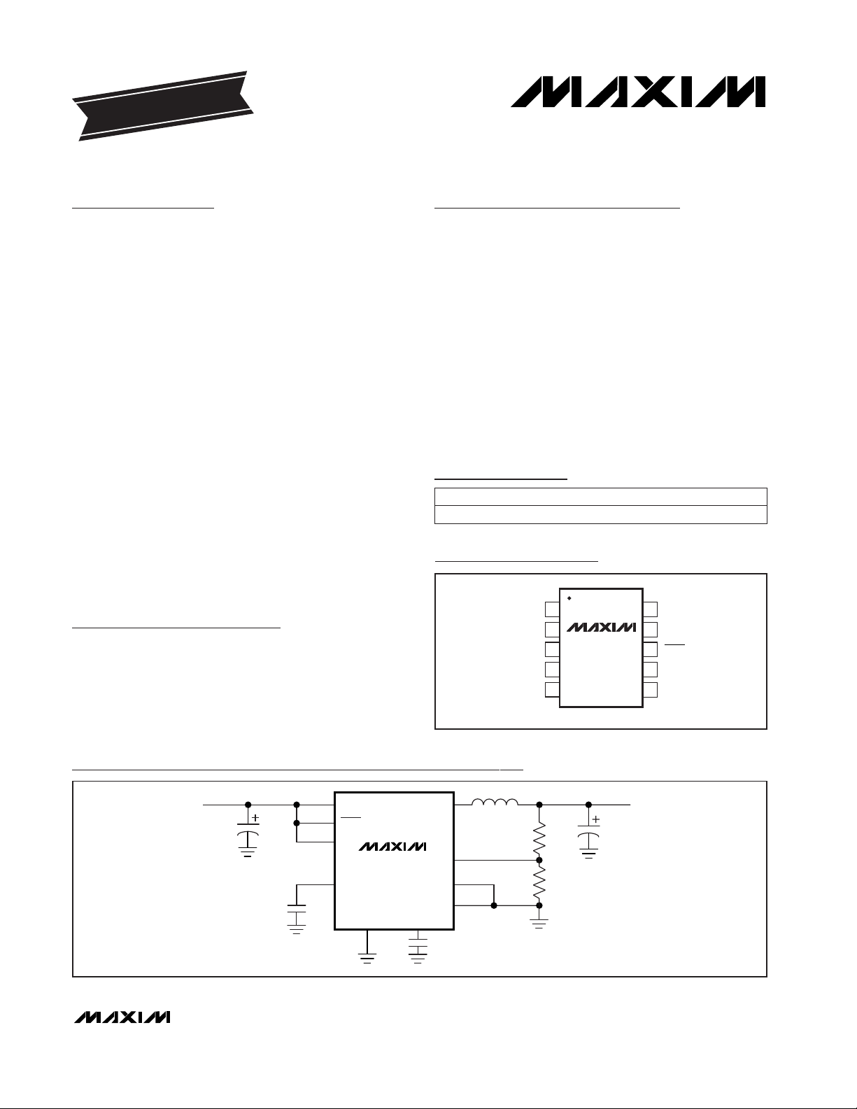
1
2
3
4
5
10
9
8
7
6
PGND
LX
SHDN
SYNC/PWMREF
GND
BP
IN
MAX1692
TOP VIEW
LIMFB
µMAX
19-1400; Rev 0; 11/98
PART
MAX1692EUB -40°C to +85°C
TEMP. RANGE PIN-PACKAGE
10 µMAX
EVALUATION KIT MANUAL
FOLLOWS DATA SHEET
Idle Mode is a trademark of Maxim Integrated Products.
Pin Configuration
Ordering Information
Typical Operating Circuit
MAX1692
FB
SYNC/PWM
PGND
BP
LIM
LX
SHDN
IN
L
C2
R1
R2
C4
C3
C1
V
IN
= 2.7V TO 5.5V V
OUT
= 1.25V TO V
IN
AGND REF
Page 2
MAX1692
Low-Noise, 5.5V-Input,
PWM Step-Down Regulator
2 _______________________________________________________________________________________
ABSOLUTE MAXIMUM RATINGS
ELECTRICAL CHARACTERISTICS
(VIN= +3.6V, SYNC/PWM = GND, V
LIM
= 3.6V, SHDN = IN, circuit of Figure 2; TA= 0°C to +85°C, unless otherwise noted. Typical
values are at T
A
= +25°C.)
Stresses beyond those listed under “Absolute Maximum Ratings” may cause permanent damage to the device. These are stress ratings only, and functional
operation of the device at these or any other conditions beyond those indicated in the operational sections of the specifications is not implied. Exposure to
absolute maximum rating conditions for extended periods may affect device reliability.
IN, BP, SHDN, SYNC/PWM, LIM to GND ................ -0.3V to +6V
BP to IN .................................................................-0.3V to +0.3V
PGND to GND ...................................................... -0.3V to +0.3V
LX to PGND................................................. -0.3V to (V
IN
+ 0.3V)
FB, REF to GND......................................... -0.3V to (V
BP
+ 0.3V)
Reference Current............................................................. ±1mA
LX Peak Current (internally limited)...................................... 1.6A
Continuous Power Dissipation (T
A
= +70°C)
10-Pin µMAX (derate 5.6mW/°C above +70°C)............444mW
Operating Temperature Range .......................... -40°C to +85°C
Maximum Junction Temperature .................................... +150°C
Storage Temperature Range............................ -65°C to +160°C
Lead Temperature (soldering, 10sec).............................+300°C
(Note 1)
FB = OUT, VIN= V
LIM
= 2.7V to 5.5V,
I
OUT
= 0
SHDN = LX = GND, includes LX leakage
current
SYNC/PWM = GND, VFB= 1.4V,
LX unconnected
ILX= 180mA
SYNC/PWM = IN, FB = REF
VFB= 1.4V
VIN= 3.6V
FB = OUT, VIN= V
LIM
= 5.5V, I
OUT
= 0
(duty cycle = 23%) (Note 2)
Duty cycle = 100% to 23%
I
OUT
= 0 to 600mA, LIM = IN or
I
OUT
= 0 to 250mA, LIM = GND
LIM = IN
VFB= 1.4V
LIM = GND
CONDITIONS
µA0.1 10Shutdown Supply Current
µA85 140Quiescent Current
mA80 120 160
Pulse-Skipping Current-Limit
Threshold
0 50 100
mA
-450 -850 -1600
N-Channel Current-Limit
Threshold
0.75 1.2 1.55
A
0.35 0.6 0.85
P-Channel Current-Limit
Threshold
VV
REF
V
IN
Output Adjustment Range
1.223 1.249 1.275
V2.7 5.5V
IN
Input Voltage Range
0.5
Ω
0.4 0.8
N
RDS(ON)
N-Channel On-Resistance
0.4
Ω
0.3 0.65
P
RDS(ON)
P-Channel On-Resistance
V1.223 1.249 1.275V
FB
Feedback Voltage
%+1Line Regulation
%-1.3Load Regulation
nA-50 0.01 50I
FB
FB Input Current
UNITSMIN TYP MAXSYMBOLPARAMETER
VIN= 5.5V, VLX= 0 or 5.5V µA-20 0.1 20LX Leakage Current
kHz650 750 830f
OSC
Oscillator Frequency
kHz500 1000SYNC Capture Range
%100duty
MAX
Maximum Duty Cycle
%22duty
MIN
Minimum Duty Cycle
I
REF
= 0 V1.235 1.250 1.265V
REF
Reference Output Voltage
FB = OUT, VIN= 2.7V to 5.5V,
I
OUT
= 0 to 600mA, LIM = IN or
I
OUT
= 0 to 250mA, LIM = GND
V
1.190 1.232 1.275
V
OUT
Output Voltage
ILX= 180mA
VIN= 2.7V
VIN= 3.6V
VIN= 2.7V
Page 3
MAX1692
Low-Noise, 5.5V-Input,
PWM Step-Down Regulator
_______________________________________________________________________________________ 3
Note 1: Guaranteed by minimum and maximum duty-factor tests.
Note 2: The following equation can be used to calculate FB accuracy for output voltages other than 1.232V:
(see Feedback Voltage vs. Load Current)
V
FB
= V
FB (NOMINAL)
- (Line Reg) (V
OUT
/ VIN- 0.23) / 0.77 - (Load Reg)(I
OUT
+ 0.5 · I
RIPPLE
) / I
MAX
where: Line Reg = the line regulation
Load Reg = the load regulation
I
RIPPLE
= (1- V
OUT
/ VIN) · V
OUT
/ (f
OSC
· L) where L is the inductor value
I
MAX
= 250mA (LIM = GND) or 600mA (LIM = IN)
Note 3: Specifications to -40°C are guaranteed by design, not production tested.
ELECTRICAL CHARACTERISTICS (continued)
(VIN= +3.6V, SYNC/PWM = GND, V
LIM
= 3.6V, SHDN = IN, circuit of Figure 2; TA= 0°C to +85°C, unless otherwise noted. Typical
values are at T
A
= +25°C.)
High or low
0 ≤ I
REF
≤ 50µA
SHDN, SYNC/PWM, LIM
CONDITIONS
ns500
SYNC/PWM Minimum Pulse Width
mV3 15Reference Load Regulation
µA-1 0.1 1Logic Input Current
UNITSMIN TYP MAXSYMBOLPARAMETER
(Note 1)
FB = OUT, VIN= V
LIM
= 2.7V to 5.5V,
I
OUT
= 0
SYNC/PWM = GND, LX = unconnected,
VFB= 1.4V
FB = OUT, VIN= V
LIM
= 5.5V, I
OUT
= 0
(duty cycle = 23%) (Note 2)
VFB=1.4V
LIM = IN
CONDITIONS
VREF V
IN
Output Adjustment Range
1.213 1.285
V2.7 5.5V
IN
Input Voltage Range
µA140Quiescent Current
V1.213 1.285V
FB
Feedback Voltage
nA-50 50I
FB
FB Input Current
A
0.7 1.6
P-Channel Current-Limit
Threshold
mA
N-Channel Current-Limit
Threshold
UNITSMIN MAXSYMBOLPARAMETER
ELECTRICAL CHARACTERISTICS
(VIN= +3.6V, SYNC/PWM = GND, V
LIM
= 3.6V, SHDN = IN, circuit of Figure 2, TA= -40°C to +85°C, unless otherwise noted.) (Note 3)
LIM = GND
SYNC/PWM = IN, FB = REF -15 110
SHDN = LX = GND, includes LX leakage current
µA10Shutdown Supply Current
kHz630 840f
OSC
Oscillator Frequency
I
REF
= 0 V1.230 1.268V
REF
Reference Output Voltage
VINrising, typical hysteresis is 85mV V2.3 2.5UVLO
Undervoltage Lockout
Threshold
SHDN, SYNC/PWM, LIM
V2V
IH
Logic Input High
SHDN, SYNC/PWM, LIM
V0.4V
IL
Logic Input Low
SHDN, SYNC/PWM, LIM
µA-1 1Logic Input Current
0.3 0.9
SHDN, SYNC/PWM, LIM
V0.4V
IL
Logic Input Low
VINrising, typical hysteresis is 85mV V2.3 2.4 2.5UVLOUndervoltage Lockout Threshold
SHDN, SYNC/PWM, LIM
V2V
IH
Logic Input High
FB = OUT, VIN= 2.7V to 5.5V,
I
OUT
= 0 to 600mA, LIM = IN or
I
OUT
= 0 to 250mA, LIM = GND
V
1.185 1.285
V
OUT
Output Voltage
Page 4
1.74
1.76
1.80
1.78
1.82
1.84
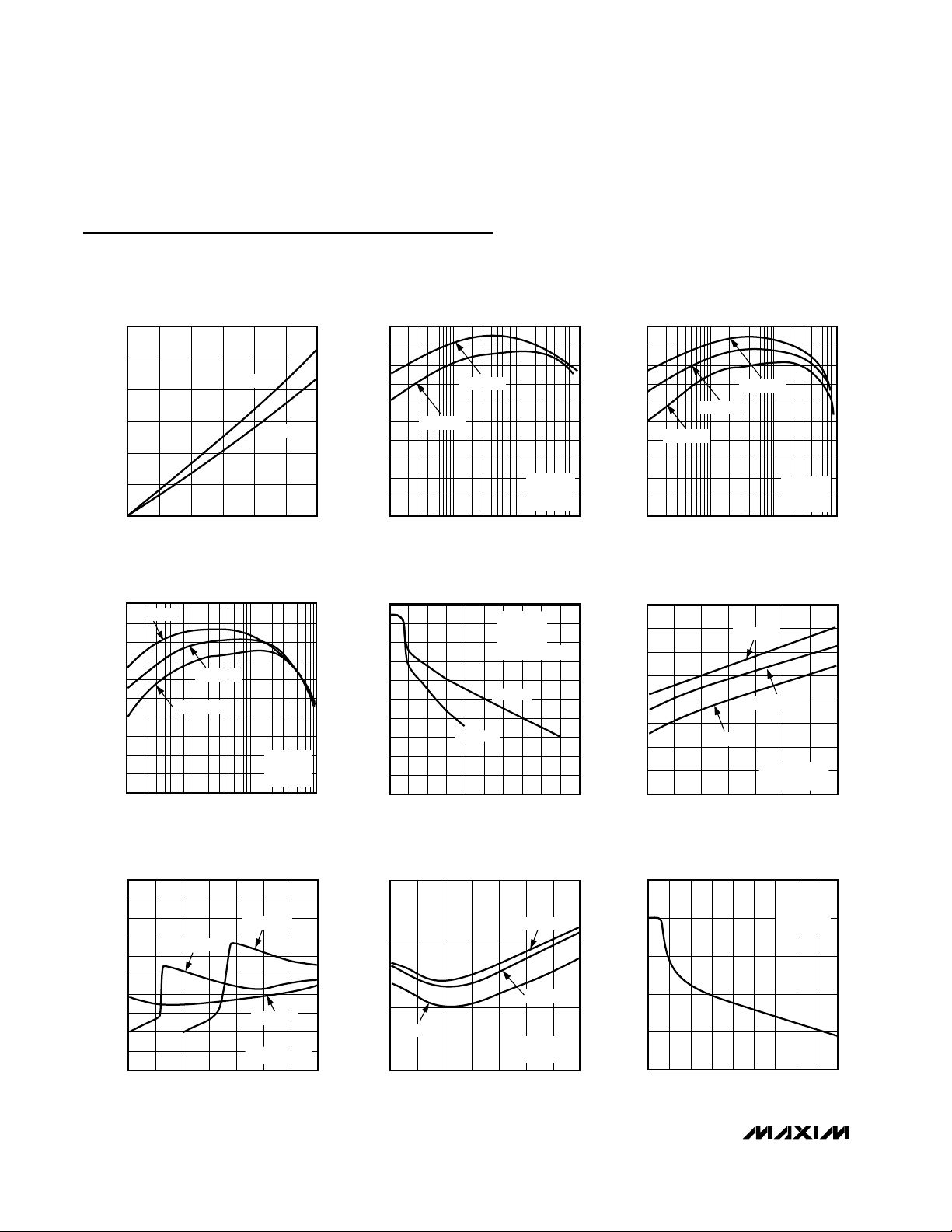
0 400300200100 500 600 700 800 900
OUTPUT VOLTAGE vs.
LOAD CURRENT
MAX1692-10
LOAD CURRENT (mA)
OUTPUT VOLTAGE (V)
VIN = 2.7V
V
OUT
= 1.8V
R1 = 138kΩ
R2 = 301kΩ
MAX1692
Low-Noise, 5.5V-Input,
PWM Step-Down Regulator
4 _______________________________________________________________________________________
0
200
100
400
300
500
600
0 300 450150 600 750 900
DROPOUT VOLTAGE vs.
LOAD CURRENT
MAX1692-01
LOAD CURRENT (mA)
DROPOUT VOLTAGE (mV)
V
OUT
= 2.5V
V
OUT
= 3.3V
95
50
1 100010010
EFFICIENCY vs. LOAD CURRENT
(V
OUT
= 3.3V)
65
55
85
75
100
70
60
90
80
MAX1692-02
LOAD CURRENT (mA)
EFFICIENCY (%)
VIN = 5.0V
VIN = 3.6V
LIM = IN
R1 = 505kΩ
R2 = 301kΩ
95
50
1 100010010
EFFICIENCY vs. LOAD CURRENT
(V
OUT
= 2.5V)
65
55
85
75
100
70
60
90
80
MAX1692-03
LOAD CURRENT (mA)
EFFICIENCY (%)
VIN = 5.0V
VIN = 2.7V
VIN = 3.6V
LIM = IN
R1 = 309kΩ
R2 = 301kΩ
95
50
1 100010010
EFFICIENCY vs. LOAD CURRENT
(V
OUT
= 1.8V)
65
55
85
75
100
70
60
90
80
MAX1692-04
LOAD CURRENT (mA)
EFFICIENCY (%)
VIN = 2.7V
VIN = 5.0V
VIN = 3.6V
LIM = IN
R1 = 138kΩ
R2 = 301kΩ
0
1.5
1.0
0.5
2.5
2.0
4.5
4.0
3.5
3.0
5.0
2.7 3.1 3.5 3.9 4.3 4.7 5.1 5.5
BATTERY INPUT CURRENT vs.
INPUT VOLTAGE
MAX1692-07
INPUT VOLTAGE (V)
BATTERY INPUT CURRENT (mA)
SYNC/PWM = IN
V
OUT
= 3.3V
V
OUT
= 1.8V
V
OUT
= 2.5V
1.2
1.21
1.205
1.225
1.22
1.215
1.245
1.24
1.235
1.23
1.25
0 300100 200 400 500 600 700 800 900 1000
FEEDBACK VOLTAGE
vs. LOAD CURRENT
MAX1692-05
LOAD CURRENT (mA)
FB VOLTAGE (V)
VIN = 5.0V
R1 = 309kΩ
R2 = 301kΩ
SYNC/PWM = GND
LIM = IN
LIM = GND
60
70
65
80
75
95
90
85
100
2.7 3.53.1 3.9 4.3 4.7 5.1 5.5
BATTERY INPUT CURRENT vs.
INPUT VOLTAGE
MAX1692-06
INPUT VOLTAGE (V)
BATTERY INPUT CURRENT (µA)
V
OUT
= 1.8V
SYNC/PWM = GND
TA = +85°C
TA = +25°C
TA = -40°C
1.0
1.5
2.0
2.5
2.7 3.1 3.5 3.9 4.3 4.7 5.1 5.5
BATTERY INPUT CURRENT vs. INPUT
VOLTAGE AND TEMPERATURE
MAX1692-09
INPUT VOLTAGE (V)
BATTERY INPUT CURRENT (mA)
V
OUT
= 1.8V
SYNC/PWM = IN
TA = +85°C
TA = +25°C
TA = -40°C
Typical Operating Characteristics
(SYNC/PWM = GND, circuit of Figure 2, L = Sumida CD43-100, TA = +25°C, unless otherwise noted.)
Page 5

MAX1692
Low-Noise, 5.5V-Input,
PWM Step-Down Regulator
_______________________________________________________________________________________
5
600
650
700
750
800
OSCILLATOR FREQUENCY vs.
SUPPLY VOLTAGE
MAX1692-11
SUPPLY VOLTAGE (V)
OSCILLATOR FREQUENCY (kHz)
TA = +85°C
TA = +25°C
TA = -40°C
I
OUT
= 200mA
2.7 3.9 4.33.1 3.5 4.7 5.1 5.5
0.5
0.8
1.1
1.4
2.7 3.9 4.33.1 3.5 4.7 5.1 5.5
MAXIMUM OUTPUT CURRENT vs.
INPUT VOLTAGE
MAX1692-12
INPUT VOLTAGE (V)
MAXIMUM OUTPUT CURRENT (A)
V
OUT
= 1.8V
LIM = IN
LIM = GND
500µs/div
LOAD-TRANSIENT RESPONSE
V
LX
5V/div
V
OUT
AC-COUPLED
100mV/div
I
OUT
2.5A/div
MAX1692-17
I
LOAD
= 30mA to 700mA
2ms/div
START-UP FROM SHUTDOWN
V
SHDN
2V/div
I
IN
0.5A/div
V
OUT
1V/div
MAX1692-14
2ms/div
HEAVY LOAD SWITCHING WAVEFORMS
VIN = 5V, V
OUT
= 3.3V, I
OUT
= 700mA
V
LX
5V/div
I
LX
0.5A/div
V
OUT
AC-
COUPLED
100mV/div
MAX1692-15
2ms/div
LINE-TRANSIENT RESPONSE
VIN = 3V to 5V, I
OUT
= 300mA
V
IN
AC-
COUPLED
2V/div
V
OUT
AC-
COUPLED
50mV/div
MAX1692-18
2ms/div
RECOVERY FROM 100% DUTY CYCLE
VIN = 3.3V to 4.5V , V
OUT
= 3.3V, I
OUT
= 500mA
V
IN
2V/div
V
LX
5V/div
V
OUT
AC-
COUPLED
500mV/div
MAX1692-19
Typical Operating Characteristics (continued)
(SYNC/PWM = GND, TA = +25°C, unless otherwise noted.)
100kHz 1MHz 10MHz
SWITCHING HARMONICS AND NOISE
1mV/div
MAX1692-22
1ms/div
I
OUT
= 500mA
Page 6

MAX1692
Low-Noise, 5.5V-Input,
PWM Step-Down Regulator
6 _______________________________________________________________________________________
NAME FUNCTION
1 IN Supply Voltage Input. Input range from +2.7V to +5.5V. Bypass with a 10µF capacitor.
2 BP
Supply Bypass Pin. Internally connected to IN. Bypass with a 0.1µF capacitor. Do not connect to an
external power source other than IN.
PIN
3 GND Ground
4 REF
1.25V, 1.2% Reference Output. Capable of delivering 50µA to external loads. Bypass with a 0.22µF capacitor to GND.
8
SHDN
Active-Low, Shutdown-Control Input. Reduces quiescent current to 0.1µA. In shutdown, output becomes
high impedance.
7
SYNC/
PWM
Oscillator Sync and Low-Noise, Mode-Control Input.
SYNC/PWM = IN (Forced PWM Mode)
SYNC/PWM = GND (PWM/PFM Mode)
An external clock signal connected to this pin allows for LX switching synchronization.
6 LIM Current-Limit Select Input. Connect LIM to GND for 0.6A current limit or LIM to IN for 1.2A current limit.
5 FB Feedback Input
10 PGND Power Ground
9 LX Inductor Connection to the Drains of the Internal Power MOSFETs
Pin Description
PFM CURRENT COMPARATOR
CONTROL AND
DRIVER LOGIC
SLOPE COMPENSATION
PWM
COMPARATOR
NEGLIM
COMPARATOR
5mV IN PFM
ADJ. IN PWM
PGND
0.1X
SENSE FET
SENSE FET
1Ω
LX
IN
P
N
BP
0.1X
1Ω
10Ω
CHIP
SUPPLY
PWM
ON
REF
FB
SYNC/
PWM
PFM
COMPARATOR
OVERVOLTAGE
COMPARATOR
PWM ON
SIGNAL
40mV
FB
REF
REF
FB
12mV
120mV
RAMP
GEN
SYNC
CELL
ON
LIM COMPARATOR
REF
GND
REF
SHDN
MAX1692
Figure 1. Simplified Functional Diagram
Page 7

MAX1692
Low-Noise, 5.5V-Input,
PWM Step-Down Regulator
_______________________________________________________________________________________ 7
Detailed Description
The MAX1692 step-down, pulse-width-modulated
(PWM), DC-DC converter has an adjustable output
range from 1.25V to the input voltage. An internal synchronous rectifier improves efficiency and eliminates an
external Schottky diode. Fixed-frequency operation
enables easy post-filtering, thereby providing excellent
noise characteristics. As a result, the MAX1692 is an
ideal choice for many small wireless systems.
The MAX1692 accepts inputs as low as +2.7V while still
delivering 600mA. The MAX1692 can operate in four
modes to optimize performance. A forced (PWM) mode
switches at a fixed frequency, regardless of load, for
easy post-filtering. A synchronizable PWM mode uses
an external clock to minimize harmonics. A PWM/PFM
mode extends battery life by operating in PWM mode
under heavy loads and PFM mode under light loads for
reduced power consumption. Shutdown mode reduces
quiescent current to 0.1µA.
PWM Control Scheme
The MAX1692 uses a slope-compensated, currentmode PWM controller capable of achieving 100% duty
cycle. The device uses an oscillator-triggered, minimum on-time, current-mode control scheme. The minimum on-time is approximately 150ns unless in dropout.
The maximum on-time is approximately 2/f
OSC
, allowing operation to 100% duty cycle. Current-mode feedback provides cycle-by-cycle current limiting for
superior load- and line-response and protection of the
internal MOSFET and rectifier.
At each falling edge of the internal oscillator, the SYNC
cell sends a PWM ON signal to the control and drive
logic, turning on the internal P-channel MOSFET (main
switch) (Figure 1). This allows current to ramp up
through the inductor (Figure 2) to the load, and stores
energy in a magnetic field. The switch remains on until
either the current-limit (LIM) comparator is tripped or
the PWM comparator signals that the output is in regulation. When the switch turns off during the second half
of each cycle, the inductor’s magnetic field collapses,
releasing the stored energy and forcing current through
the N-channel synchronous rectifier to the output-filter
capacitor and load. The output-filter capacitor stores
charge when the inductor current is high and releases
it when the inductor current is low, thus smoothing the
voltage across the load.
During normal operation, the MAX1692 regulates output voltage by switching at a constant frequency and
then modulating the power transferred to the load each
cycle using the PWM comparator. A multi-input comparator sums three weighted differential signals: the
output voltage with respect to the reference, the main
switch current sense, and the slope-compensation
ramp. It modulates output power by adjusting the
inductor-peak current during the first half of each cycle,
based on the output-error voltage. The MAX1692’s loop
gain is relatively low to enable the use of a small, lowvalued output-filter capacitor. The resulting load regulation is 1.3% (typ) at 0 to 600mA.
100% Duty-Cycle Operation
The maximum on-time can exceed one internal oscillator cycle, which permits operation up to 100% duty
cycle. As the input voltage drops, the duty cycle
increases until the P-channel MOSFET is held on continuously. Dropout voltage in 100% duty cycle is the
output current multiplied by the on-resistance of the
internal switch and inductor, around 280mV (I
OUT
=
600mA). In PWM mode, subharmonic oscillation can
occur near dropout but subharmonic voltage ripple is
small, since the ripple current is low.
Synchronous Rectification
An N-channel, synchronous-rectifier improves efficiency during the second half of each cycle (off time).
When the inductor current ramps below the threshold
set by the NEGLIM comparator (Figure 1) or when the
PWM reaches the end of the oscillator period, the synchronous rectifier turns off. This keeps excess current
from flowing backward through the inductor, from the
output-filter capacitor to GND, or through the switch
and synchronous rectifier to GND. During PWM operation, the NEGLIM threshold adjusts to permit small
LX
FB
IN
LIM
REF
BP
MAX1692
C1
10µF
V
IN
+2.7V TO +5.5V
L1
10µH
V
OUT
= 1.8V @ 600mA
C5
47pFR1138k
R2
300k
C2
47µF
ON
/
OFF
C4
0.22µF
C3
0.1µF
GND PGND
SYNC/
PWM
SHDN
Figure 2. Standard Application Circuit
Page 8

MAX1692
Low-Noise, 5.5V-Input,
PWM Step-Down Regulator
8 _______________________________________________________________________________________
amounts of reverse current to flow from the output during light loads. This allows regulation with a constantswitching frequency and eliminates minimum load
requirements. The NEGLIM comparator threshold is
50mA if VFB< 1.25V, and decreases as VFBexceeds
1.25V to prevent the output from rising. The NEGLIM
threshold in PFM mode is fixed at 50mA. (See
Forced
PWM and PWM/PFM Operation
section.)
Forced PWM and PWM/PFM Operation
Connect SYNC/PWM to IN for normal forced PWM
operation. Forced PWM operation is desirable in sensitive RF and data-acquisition applications, to ensure that
switching-noise harmonics do not interfere with sensitive IF and data-sampling frequencies. A minimum load
is not required during forced PWM operation, since the
synchronous rectifier passes reverse-inductor current
as needed to allow constant-frequency operation with
no load. Forced PWM operation uses higher supply
current with no load (2mA typ).
Connecting SYNC/PWM to GND enables PWM/PFM
operation. This proprietary control scheme overrides
PWM mode and places the MAX1692 in PFM mode at
light loads to improve efficiency and reduce quiescent
current to 85µA. With PWM/PFM enabled, the MAX1692
initiates pulse-skipping PFM operation when the peak
inductor current drops below 120mA. During PFM operation, the MAX1692 switches only as needed to service
the load, reducing the switching frequency and associated losses in the internal switch, the synchronous rectifier, and the external inductor.
During PFM mode, a switching cycle initiates when the
PFM comparator senses that the output voltage has
dropped too low. The P-channel MOSFET switch turns
on and conducts current to the output-filter capacitor
and load until the inductor current reaches the PFM
peak current limit (120mA). Then the switch turns off
and the magnetic field in the inductor collapses, forcing
current through the synchronous rectifier to the output
filter capacitor and load. Then the MAX1692 waits until
the PFM comparator senses a low output voltage again.
The PFM current comparator controls both entry into
PWM mode and the peak switching current during PFM
mode. Consequently, some jitter is normal during transition from PFM to PWM modes with loads around
100mA, and it has no adverse impact on regulation.
Output ripple is higher during PFM operation. A larger
output-filter capacitor can be used to minimize ripple.
SYNC Input and Frequency Control
The MAX1692’s internal oscillator is set for a fixedswitching frequency of 750kHz or can be synchronized
to an external clock. Connect SYNC to IN for forcedPWM operation. Do not leave SYNC/PWM unconnected. Connecting SYNC/PWM to GND enables PWM/PFM
operation to reduce supply current at light loads.
SYNC/PWM is a negative-edge triggered input that
allows synchronization to an external frequency ranging
between 500kHz and 1000kHz. When SYNC/PWM is
clocked by an external signal, the converter operates in
forced PWM mode. If SYNC is low or high for more than
100µs, the oscillator defaults to 750kHz.
Shutdown Mode
Connecting SHDN to GND places the MAX1692 in
shutdown mode. In shutdown, the reference, control
circuitry, internal switching MOSFET, and the synchronous rectifier turn off and the output falls to 0V. Connect
SHDN to IN for normal operation.
Current-Sense Comparators
The MAX1692 uses several internal current-sense comparators. In PWM operation, the PWM comparator sets
the cycle-by-cycle current limit (Figure 1) and provides
improved load and line response, allowing tighter specification of the inductor-saturation current limit to
reduce inductor cost. A second 120mA current-sense
comparator used across the P-channel switch controls
entry into PFM mode. A third current-sense comparator
monitors current through the internal N-channel MOSFET
to set the NEGLIM threshold and determine when to turn
off the synchronous rectifier. A fourth comparator (LIM)
used at the P-channel MOSFET switch detects overcurrent. This protects the system, external components, and
internal MOSFETs under overload conditions.
Applications Information
Output Voltage Selection
Select an output voltage between 1.25V and VINby
connecting FB to a resistor-divider between the output
and GND (Figure 2). Select feedback resistor R2 in the
5kΩ to 500kΩ range. R1 is then given by:
R1 = R2 [(V
OUT
/ VFB) - 1]
where V
FB
= 1.232V (See Note 2 of the
Electrical
Characteristics
). Add a small ceramic capacitor (C5)
around 47pF to 100pF in parallel with R1 to compensate
for stray capacitance at the FB pin and output capacitor
equivalent series resistance (ESR).
Page 9

MAX1692
Low-Noise, 5.5V-Input,
PWM Step-Down Regulator
_______________________________________________________________________________________ 9
Capacitor Selection
Choose input- and output-filter capacitors to service
inductor currents with acceptable voltage ripple. The
input-filter capacitor also reduces peak currents and
noise at the voltage source. In addition, connect a lowESR bulk capacitor (>10µF suggested) to the input.
Select this bulk capacitor to meet the input ripple
requirements and voltage rating, rather than capacitor
size. Use the following equation to calculate the maximum RMS input current:
I
RMS
= I
OUT[VOUT(VIN
- V
OUT
)]
1/2
· V
IN
When selecting an output capacitor, consider the output-ripple voltage and approximate it as the product of
the ripple current and the ESR of the output capacitor.
V
RIPPLE
= [V
OUT(VIN
- V
OUT
)] /
[2 · f
OSC
(L) (VIN)] · ESR
C2
where ESRC2is the equivalent-series resistance of the
output capacitor.
The MAX1692’s loop gain is relatively low, enabling the
use of small, low-value output filter capacitors. Higher
values provide improved output ripple and transient
response. Lower oscillator frequencies require a largervalue output capacitor. When PWM/PFM is used, verify
capacitor selection with light loads during PFM operation, since output ripple is higher under these conditions. Low-ESR capacitors are recommended.
Capacitor ESR is a major contributor to output ripple
(usually more than 60%). Ordinary aluminum-electrolytic capacitors have high ESR and should be avoided.
Low-ESR aluminum-electrolytic capacitors are acceptable and relatively inexpensive. Low-ESR tantalum
capacitors are better and provide a compact solution
for space-constrained surface-mount designs. Do not
exceed the ripple-current ratings of tantalum capacitors. Ceramic capacitors have the lowest ESR overall,
and OS-CON™capacitors have the lowest ESR of the
high-value electrolytic types.
It is generally not necessary to use ceramic or OS-CON
capacitors for the MAX1692; consider them only in very
compact, high-reliability, or wide-temperature applications where the expense is justified. When using verylow-ESR capacitors, such as ceramic or OS-CON,
check for stability while examining load-transient
response. The output capacitor is determined by ensuring that the minimum capacitance value and maximum
ESR values are met:
C2 > 2V
REF
(1 + V
OUT/VIN(MIN)
) / (V
OUT
· R
SENSE
· f
OSC
)
R
ESR
< (R
SENSE
)(V
OUT
) / (V
REF
)
where C2 is the output filter capacitor, V
REF
is the internal reference voltage of 1.25V, VIN(min) is the minimum
input voltage (2.7V), R
SENSE
is the internal sense resis-
tance of 0.1Ω, and f
OSC
is the internal oscillator frequency (typically 750kHz). These equations provide the
minimum requirements. The value of C2 may need to
be increased for operation at duty-cycle extremes.
Tables 1 and 2 provide recommended inductor and
capacitor sizes at various external sync frequencies.
Table 3 lists suppliers for the various components used
with the MAX1692.
Standard Application Circuits
Figures 2 and 3 are standard application circuits optimized for power and board space respectively. The circuit of Figure 2 is the most general of the two, and
generates 1.8V at 600mA.
The circuit of Figure 3 is optimized for smallest overall
size. Cellular phones are using low voltage for baseband logic and have critical area and height restrictions. This circuit operates from a single Li-ion battery
(2.9V to 4.5V) and delivers up to 200mA at 1.8V. It uses
small ceramic capacitors at the input and output and a
tiny chip inductor such as the NLC322522T series from
TDK. With the MAX1692 in a 10-pin µMAX package, the
entire circuit can fit in only 60mm2and have less than
2.4mm height.
LX
FB
IN
BP
REF
LIM
MAX1692
C5
4.7µF
V
IN
+2.9V TO +4.5V
L1
10µH
V
OUT
= 1.8V @ 200mA
C5
47pF
R1
138k
R2
301k
10µF
10µF
ON
/
OFF
C4
0.1µF
GND PGND
SYNC/
PWM
SHDN
C2
Figure 3. Miniaturized 200mA Output Circuit Fits in 60mm
2
OS-CON is a trademark of Sanyo Corp.
Page 10

MAX1692
Low-Noise, 5.5V-Input,
PWM Step-Down Regulator
10 ______________________________________________________________________________________
Bypass Considerations
Bypass IN and OUT to PGND with 10µF and 47µF,
respectively. Bypass BP and REF to GND with 0.1µF
and 0.22µF, respectively. Locate the bypass capacitors
as close as possible to their respective pins to minimize
noise coupling. For optimum performance, place input
and output capacitors as close to the device as feasible (see
Capacitor Selection
section).
PC Board Layout and Routing
High switching frequencies and large peak currents
make PC board layout a very important part of design.
Good design minimizes excessive EMI on the feedback
paths and voltage gradients in the ground plane, both
of which can result in instability or regulation errors.
Connect the inductor, input filter capacitor, and output
filter capacitor as close together as possible, and keep
their traces short, direct, and wide. Connect their
ground pins at a single common node in a star-ground
configuration. The external voltage-feedback network
should be very close to the FB pin, within 0.2in (5mm).
Keep noisy traces, such as from the LX pin, away from
the voltage-feedback network; also keep them separate, using grounded copper. Connect GND and PGND
at the highest quality ground. The MAX1692 evaluation
kit manual illustrates an example PC board layout and
routing scheme.
FAXCOMPANY
Coilcraft 847-639-6400
PHONE
AVX 843-946-0238
847-639-1469
843-626-3123
Coiltronics 561-241-7876 561-241-9339
Kemet 408-986-0424 408-986-1442
Table 2. Suggested Capacitors
Nihon
USA 805- 867-2555
Japan 81-3-3494-7411
805- 867-2698
81-3-3494-7414
Sanyo
USA 619-661-6835
Japan 81-7-2070-6306
619-661-1055
81-7-2070-1174
Sprague 603-224-1961 603- 224-1430
Sumida
USA 847-956-0666
Japan 81-3-3607-5111
847- 956-0702
81-3-3607-5144
Taiyo Yuden 408-573-4150 408-573-4159
TDK 847-390-4373 847-390-4428
Table 1. Suggested Inductors
Table 3. Component Suppliers
SUGGESTED
INDUCTORS
OUTPUT
VOLTAGE
RANGE
(V)
INDUCTOR L
VALUE
(µH)
1.25 to 2.5 10
Sumida CD43-100
Coilcraft D01608C-103
Sumida CD54-100
TDK NLC322522-100T
2.5 to 4.0 22
Sumida CD43-220
Sumida CD54-220
4.0 to 5.5 33
Sumida CD43-330
Sumida CD54-330
ESR
(mΩ)
Sanyo
6TPA47M
MANUFACTURER
PART NUMBER
AVX
TPSD476M016R0150
100
150
Sprague
594D686X9010C2T
95
Taiyo Yuden
JMK325BJ106MN
50
Poscap
TYPE
Tantalum
Tantalum
Ceramic
Page 11

MAX1692
Low-Noise, 5.5V-Input,
PWM Step-Down Regulator
______________________________________________________________________________________ 11
Package Information
10LUMAXB.EPS
TRANSISTOR COUNT: 1462
Chip Information
Page 12

MAX1692
Low-Noise, 5.5V-Input,
PWM Step-Down Regulator
Maxim cannot assume responsibility for use of any circuitry other than circuitry entirely embodied in a Maxim product. No circuit patent licenses are
implied. Maxim reserves the right to change the circuitry and specifications without notice at any time.
12
____________________Maxim Integrated Products, 120 San Gabriel Drive, Sunnyvale, CA 94086 408-737-7600
© 1998 Maxim Integrated Products Printed USA is a registered trademark of Maxim Integrated Products.
NOTES
 Loading...