

Page 1
19-4964; Rev 0; 9/09
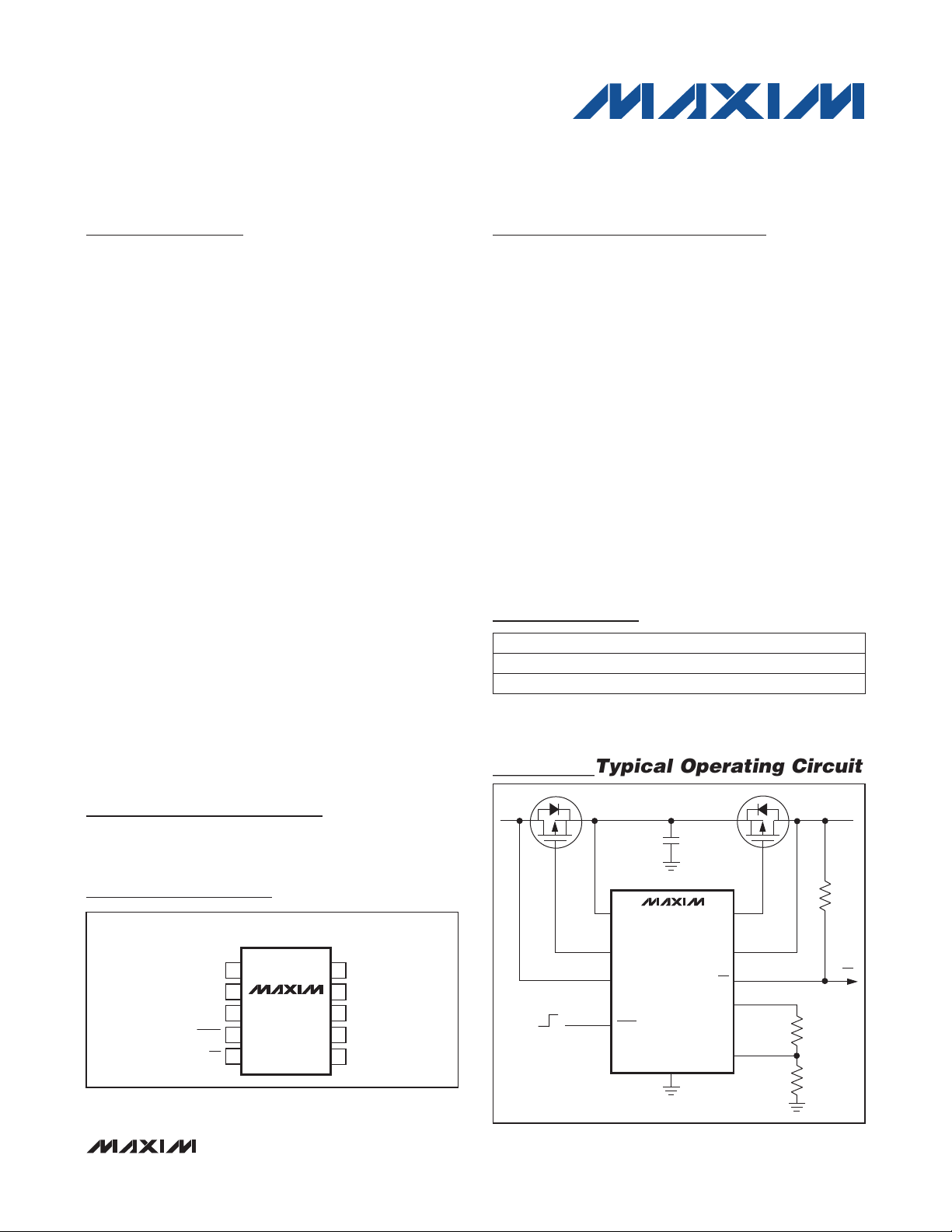
Typical Operating Circuit
Ideal Diode, Reverse-Battery, and Overvoltage Protection
Switch/Limiter Controllers with External MOSFETs
General Description
The MAX16914/MAX16915 low-quiescent-current overvoltage and reverse-battery protection controllers are
designed for automotive and industrial systems that
must tolerate high-voltage transient and fault conditions.
These conditions include load dumps, voltage dips, and
reversed input voltages. The controllers monitor the input
voltage on the supply line and control two external pFETs
to isolate the load from the fault condition. The external
pFETs are turned on when the input supply exceeds
4.5V and stay on up to the programmed overvoltage
threshold. During high-voltage fault conditions, the controllers regulate the output voltage to the set upper
threshold voltage (MAX16915), or switch to high resistance (MAX16914) for the duration of the overvoltage
transient to prevent damage to the downstream circuitry.
The overvoltage event is indicated through an active-low,
open-drain output, OV.
The reverse-battery pFET behaves as an ideal diode,
minimizing the voltage drop when forward biased. Under
reverse bias conditions, the pFET is turned off, preventing a downstream tank capacitor from being discharged
into the source.
Shutdown control turns off the IC completely, disconnecting the input from the output and disconnecting
TERM from its external resistor-divider to reduce the
quiescent current to a minimum.
Both devices are available in a 10-pin FMAXM package
and operate over the automotive -40NC to +125NC temperature range.
Features
S 4.5V to 19V Input Voltage Operation
S Transient Voltage Protection Up to +44V and -75V
S Adjustable Overvoltage Limit with Resistor-
Divider Shut Off in Shutdown
S Ideal Diode Reverse-Battery Protection
S Low Voltage Drop When Used with Properly Sized
External pFETs
S Back-Charge Prevention
S Overvoltage Indicator
S Shutdown Input
S 29µA Low Operating Current
S 6µA Low Shutdown Current
S Thermal-Overload Protection
S -40NC to +125NC Operating Temperature Range
S Small 10-Pin µMAX Package
S AEC-Q100 Qualified
Ordering Information
PART TEMP RANGE PIN-PACKAGE
MAX16914AUB/V+ -40NC to +125NC 10 FMAX
MAX16915AUB/V+ -40NC to +125NC 10 FMAX
+Denotes a lead(Pb)-free/RoHS-compliant package.
/V denotes an automotive qualified device.
MAX16914/MAX16915
Applications
Automotive
Industrial
Pin Configuration
TOP VIEW
+
1
V
CC
2
GATE1
SENSE IN
µMAX is a registered trademark of Maxim Integrated Products, Inc.
_______________________________________________________________ Maxim Integrated Products 1
3
4
5
MAX16914
MAX16915
10
9
8
7
6
GATE2
SENSE OUT
TERM
SETSHDN
GNDOV
For pricing, delivery, and ordering information, please contact Maxim Direct at 1-888-629-4642,
or visit Maxim’s website at www.maxim-ic.com.
V
BATT
OFF
V
CC
MAX16914
MAX16915
GATE1
SENSE IN
ON
SHDN
GND
GATE2
SENSE OUT
OV
TERM
SET
P2P1
V
OUT
OV
R1
R2
Page 2

Ideal Diode, Reverse-Battery, and Overvoltage Protection
Switch/Limiter Controllers with External MOSFETs
ABSOLUTE MAXIMUM RATINGS
VCC, SENSE OUT, TERM, SHDN, OV to GND for
P 400ms ............................................................. -0.3V to +44V
VCC, SENSE OUT, TERM, SHDN, OV to GND
for P 90s .............................................................-0.3V to +28V
VCC, SENSE OUT, TERM, SHDN, OV to GND .....-0.3V to +20V
SENSE IN to GND for P 2ms ..................................-75V to +44V
SENSE IN to GND for P 90s ..................................-18V to +44V
SENSE IN to GND .................................................-0.3V to +20V
GATE1, GATE2 to VCC ..........................................-16V to +0.3V
Note 1: Package thermal resistances were obtained using the method described in JEDEC specification JESD51-7, using a four-
layer board. For detailed information on package thermal considerations, refer to www.maxim-ic.com/thermal-tutorial.
Stresses beyond those listed under “Absolute Maximum Ratings” may cause permanent damage to the device. These are stress ratings only, and functional
operation of the device at these or any other conditions beyond those indicated in the operational sections of the specifications is not implied. Exposure to absolute
maximum rating conditions for extended periods may affect device reliability.
ELECTRICAL CHARACTERISTICS
(VCC = 14V, C
values are at TA = +25NC.) (Note 2)
GATE1
= 32nF, C
= 32nF, SHDN = high, TA = -40NC to +125NC, unless otherwise noted. Typical
GATE2
GATE1, GATE2 to GND ........................... -0.3V to (VCC + 0.3V)
SET to GND .............................................................-0.3V to +8V
Continuous Power Dissipation (TA = +70NC)
10-Pin FMAX (derate 8.8mW/NC above TA = +70NC)
(Note 1) .......................................................................707mW
Operating Temperature Range ........................ -40NC to +125NC
Junction Temperature .....................................................+150NC
Storage Temperature Range ............................ -65NC to +150NC
Lead Temperature (soldering, 10s) ................................+300NC
MAX16914/MAX16915
Operating Voltage Range V
Shutdown Supply Current
(I
SENSE IN
I
SHDN
Quiescent Supply Current
(I
SENSE IN
I
SHDN
VCC Undervoltage Lockout V
VCC Undervoltage-Lockout
Hysteresis
SET Threshold Voltage V
SET Threshold Voltage
Hysteresis
SET Input Current I
SHDN Low Threshold V
SHDN High Threshold V
SHDN Pulldown Current I
VCC to GATE Output Low
Voltage
VCC to GATE Clamp Voltage V
PARAMETER SYMBOL CONDITIONS MIN TYP MAX UNITS
(Note 3) 4.5 19 V
SHDN = low,
V
SENSE OUT
V
TERM
SHDN = high
V
CC
V
SET
V
SET
V
SHDN
VCC = 14V 6.25 7.5 8.5 V
VCC = 42V 14 V
+ I
+ I
+ I
SENSE OUT
)
VCC
+ I
SENSE OUT
)
VCC
+ IOV +
+ IOV +
CC
I
SHDN
I
UVLO
SETTH
V
SETHY
SET
SHDNL
SHDNH
SHDN
V
GVCC1
GVCC2
Q
TA = +25NC 6.0 12
TA = +85NC (Note
= 0V,
= 0V
rising, V
rising -3% +1.20 +3% V
= 1V 0.02 0.2 FA
SET
= 14V, internally pulled to GND 0.5 1.0 FA
3)
TA = +125NC
(Note 3)
TA = +25NC 29 53
TA = +85NC (Note
3)
TA = +125NC
(Note 3)
= 1V , SHDN = high 4.06 4.35 V
1.4 V
6.1 12
6.2 12
30 55
31 57
8 %
4 %
0.4 V
FA
FA
2 ______________________________________________________________________________________
Page 3

Ideal Diode, Reverse-Battery, and Overvoltage Protection
Switch/Limiter Controllers with External MOSFETs
ELECTRICAL CHARACTERISTICS (continued)
(VCC = 14V, C
values are at TA = +25NC.) (Note 2)
PARAMETER SYMBOL CONDITIONS MIN TYP MAX UNITS
TERM On-Resistance R
TERM Output Current I
Back-Charge Voltage Fault
Threshold
Back-Charge Voltage Threshold
Hysteresis
Back-Charge Turn-Off Time
(GATE1)
Back-Charge Recovery Time
(GATE1)
GATE2 Turn-Off Time
GATE2 Turn-On Time
Startup Response Time
(V
Rising)
SHDN
Startup Response Time
(VCC Rising)
Reverse-Battery Voltage Turn-Off
Time/UVLO Turn-Off Time
Thermal-Shutdown Temperature +170 NC
Thermal-Shutdown Hysteresis 20 NC
OV Output Low Voltage V
OV Open-Drain Leakage Current I
SENSE IN Input Current I
SENSE OUT Input Current I
SET to OV Output Low
Propagation Delay
Note 2: All parameters are production tested at TA = +25NC. Limits over the operating temperature range are guaranteed by
design and characterization.
Note 3: Guaranteed by design and characterization.
Note 4: The back-charge voltage, VBC, is defined as the voltage at SENSE OUT minus the voltage at SENSE IN.
Note 5: Defined as the time from when VBC exceeds V
Note 6: Defined as the time from when VBC falls below V
Note 7: Defined as the time from when V
Note 8: Defined as the time from when V
Note 9: The external pFETs can turn on t
Note 10: Defined as the time from when VCC exceeds the undervoltage-lockout threshold (4.3V max) to when V
fall below 1V.
Note 11: Defined as the time from when V
GATE1
= 32nF, C
= 32nF, SHDN = high, TA = -40NC to +125NC, unless otherwise noted. Typical
GATE2
TERM
TERM
V
BCTH
V
BCHY
t
BC
SHDN = high 150 500
SHDN = low, V
V
SENSE OUT
V
SENSE OUT
= 14V (Note 4) 18 25 32 mV
= 14V 50 mV
VCC = 9.5V, V
V
SENSE OUT
stepped from 4.9V to 9.5V
= 0V 1.0 FA
TERM
SENSE IN
= 9V,
6 10 Fs
(Note 5)
t
BCREC
VCC = 9.5V, V
V
SENSE OUT
SENSE IN
stepped from 9.5V to 4.9V
= 9V,
18 30 Fs
(Note 6)
t
START1
t
START2
t
REVERSE
VCC = 9.5V, V
1.5V (Note 7)
VCC = 9.5V, V
1V (Note 8)
VCC = 9.5V, from V
V
falling (Note 9)
GATE_
VCC rising from 2V to 4.5V, SHDN =
high (Note 10)
VCC and V
to 3.25V, V
rising from 1V to
SET
falling from 1.5V to
SET
SHDN
SENSE IN
SENSE OUT
falling from 4.25V
= 4.25V
rising to
3 Fs
20 Fs
100 Fs
0.150 ms
30 Fs
(Note 11)
I
OVBL
OVB
SENSE IN
SENSE OUTVSHDN
t
OVBPD
exceeds V
SET
falls below V
SET
after the IC is powered up and all input conditions are valid.
START
falls below V
CC
= 600FA 0.4 V
SINK
V
= 1.0V 1.0 FA
SET
V
= 0/14V 1 5 FA
SHDN
= 0/14V 2 5 FA
VCC = 9.5V, V
1.5V to V
OV
(25mV typ) to when V
BCTH
BCTH
(1.20V typ) to when V
SETTH
SETTH
SENSE OUT
rising from 1V to
SET
falling
GATE1
- 50mV to when V
GATE1
GATE2
- 5% (1.14V typ) to when V
- 25mV to when V
3 Fs
exceeds VCC - 3.5V.
falls below VCC - 3.5V.
exceeds VCC - 3.5V.
falls below VCC - 3.5V.
GATE2
reaches VCC - 1.75V.
GATE1
GATE1
and V
I
GATE2
MAX16914/MAX16915
_______________________________________________________________________________________ 3
Page 4

Ideal Diode, Reverse-Battery, and Overvoltage Protection
Switch/Limiter Controllers with External MOSFETs
Typical Operating Characteristics
(VCC = 14V, V
30
25
20
SUPPLY CURRENT (µA)
TERM = OPEN
15
SHDN = HIGH
SET = 0V
NO LOAD
10
4.5 19.0
MAX16914/MAX16915
4.3
4.2
4.1
4.0
3.9
3.8
UVLO TRESHOLD (V)
3.7
3.6
3.5
-40 125
14V
0V
14V
0V
100µF INPUT CAPACITOR, 122µF
OUTPUT CAPACITOR, R
= 14V, MAX16914/MAX16915 Evaluation Kit, TA = +25NC, unless otherwise noted.)
SHDN
SUPPLY CURRENT
vs. SUPPLY VOLTAGE
SUPPLY CURRENT
vs. TEMPERATURE
40
MAX16914
35
MAX16915
MAX16914 toc01
30
MAX16914
MAX16914 toc02
25
MAX16915
20
SUPPLY CURRENT (FA)
TERM = OPEN
SHDN = HIGH
15
SET = 0V, VCC = 14V
NO LOAD
17.012.0 14.59.57.0
SUPPLY VOLTAGE (V)
UVLO THRESHOLD
vs. TEMPERATURE
10
-40 125
TEMPERATURE (NC)
SET THRESHOLD
vs. TEMPERATURE
11085603510-15
1.25
RISING
MAX16914 toc04
RISING
MAX16914 toc05
1.20
1.15
SET THRESHOLD (V)
FALLING
FALLING
1.10
TEMPERATURE (NC)
STARTUP FROM
SHUTDOWN RESPONSE
20µs/div
= 100I
OUT
11085-15 10 35 60
MAX16914 toc07
-40 125
OVERVOLTAGE LIMITER RESPONSE
V
30V
SHDN
2V/div
14V
V
OUT
10V/div
14V
14V
V
GATE1
10V/div
V
GATE2
10V/div
0V
V
= 14V TO 30V
CC
TRIP THRESHOLD = 22V
100µF INPUT CAPACITOR, 22µF
OUTPUT CAPACITOR, R
COV = 10nF
TEMPERATURE (NC)
(MAX16915)
400µs/div
= 100I
OUT
11085603510-15
MAX16914 toc08
V
CC
20V/div
V
OUT
20V/div
V
OV
20V/div
V
GATE2
20V/div
SHUTDOWN SUPPLY CURRENT
vs. SUPPLY VOLTAGE
10
8
6
MAX16914
4
SUPPLY CURRENT (FA)
MAX16915
2
SHDN = LOW
SET = 0V
0
4.5 19.0
SUPPLY VOLTAGE (V)
POWER-UP RESPONSE
22µF INPUT AND OUTPUT CAPACITOR,
R
= 100I, SHDN = HIGH
OUT
40µs/div
OVERVOLTAGE SWITCH-OFF
RESPONSE (MAX16914)
30V
14V
20V
14V
0V
14V
30V
0V
VCC = 14V TO 30V
TRIP THRESHOLD = 22V
100µF INPUT CAPACITOR, 22µF
OUTPUT CAPACITOR, R
1.0µs/div
OUT
= 100I
17.014.512.09.57.0
MAX16914 toc06
MAX16914 toc09
MAX16914 toc03
V
CC
10V/div
V
OUT
10V/div
V
GATE1
10V/div
V
GATE2
10V/div
V
CC
10V/div
V
OUT
10V/div
V
OV
20V/div
V
GATE2
20V/div
4 ______________________________________________________________________________________
Page 5

Ideal Diode, Reverse-Battery, and Overvoltage Protection
Switch/Limiter Controllers with External MOSFETs
Typical Operating Characteristics (continued)
(VCC = 14V, V
= 14V, MAX16914/MAX16915 Evaluation Kit, TA = +25NC, unless otherwise noted.)
SHDN
MAX16914/MAX16915
BACK-CHARGE RESPONSE
5V
5V
0V
2.2µF INPUT CAPACITOR, 400I
INPUT RESISTOR, 22µF OUTPUT CAPACITOR
1.0µs/div
MAX16914 toc10
V
CC
5V/div
V
OUT
5V/div
V
GATE1
5V/div
VCC - V
GATE_
vs. INPUT VOLTAGE
15.0
13.5
12.0
10.5
9.0
7.5
6.0
4.5
GATE DRIVE VOLTAGE (V)
3.0
1.5
0
4.5 44.0
GATE1
GATE2
SET = GND
SHDN = HIGH
SUPPLY VOLTAGE (V)
6.6
MAX16914 toc11
6.5
6.4
GATE-DRIVE VOLTAGE (V)
6.3
6.2
40.536.027.0 31.513.5 18.0 22.59.0
-40 125
GATE-DRIVE VOLTAGE
vs. TEMPERATURE
GATE1
GATE2
VCC = 14V
SET = GND
SHDN = HIGH
11085603510-15
TEMPERATURE (NC)
Pin Description
PIN NAME FUNCTION
1 V
CC
2 GATE1
3 SENSE IN
4 SHDN
5 OV
6 GND Ground
7 SET
8 TERM
9 SENSE OUT
10 GATE2
Positive Supply Input Voltage. Bypass VCC to GND with a 0.1FF or greater ceramic capacitor.
Gate-Driver Output. Connect GATE1 to the gate of an external p-channel FET pass switch to provide low drain-to-source voltage drop, reverse voltage protection, and back-charge prevention.
Differential Voltage Sense Input (Input Side of IC). Used with SENSE OUT to provide back-charge
prevention when the SENSE IN voltage falls below the SENSE OUT voltage by 25mV.
Active-Low Shutdown/Wake Input. Drive SHDN high to turn on the voltage detectors. GATE2 is
shorted to VCC when SHDN is low. SHDN is internally pulled to GND through a 0.5FA current sink.
Connect SHDN to VCC for always-on operation.
Open-Drain Overvoltage Indicator Output. Connect a pullup resistor from OV to a positive supply
such as VCC. OV is pulled low when the voltage at SET exceeds the internal threshold.
Controller Overvoltage Threshold Programming Input. Connect SET to the center of an external
resistive divider network between TERM and GND to adjust the desired overvoltage switch-off or
limiter threshold.
Voltage-Divider Termination Output. TERM is internally connected to SENSE OUT in the MAX16915
and to VCC in the MAX16914. TERM is high impedance when SHDN is low, forcing the current to
zero in the resistor-divider connected to TERM.
Differential Voltage Sense Input (Output Side Of IC). Used with SENSE IN to provide back-charge
prevention when the SENSE IN voltage falls below the SENSE OUT voltage by 25mV.
Gate-Driver Output. Connect GATE2 to the gate of an external p-channel FET pass switch. GATE2
is driven low during normal operation and quickly regulated or shorted to VCC during an overvoltage condition. GATE2 is shorted to VCC when SHDN is low.
MAX16914 toc12
_______________________________________________________________________________________ 5
Page 6

Ideal Diode, Reverse-Battery, and Overvoltage Protection
Switch/Limiter Controllers with External MOSFETs
Functional Diagram
V
CC
GATE1
SENSE IN
REG
MAX16914/MAX16915
SHDN
OV
OV1
BANDGAP
BIAS
MAX16914
MAX16915
1.20V
TERM
SWITCH
OV1
TO V
FOR
CC
MAX16914
TO SENSE OUT
FOR MAX16915
GATE2
SENSE OUT
SET
TERM
GND
Detailed Description
The MAX16914/MAX16915 are ultra-small, low-quiescent, high load-current, overvoltage-protection circuits
for automotive or industrial applications. These devices
monitor the input and output voltages and control two
p-channel MOSFETs to protect downstream loads from
reverse-battery, overvoltage, and high-voltage transient
conditions and prevent downstream tank capacitors
from discharging into the source (back-charging).
One MOSFET (P1) eliminates the need for external
diodes, thus minimizing the input voltage drop and
In the MAX16914, the input voltage is monitored (TERM
is internally shorted to VCC—see the Functional Diagram)
making the device an overvoltage switch-off controller.
As the VCC voltage rises, and the programmed overvoltage threshold is tripped, the internal fast comparator
turns off the external p-channel MOSFET (P2), pulling
GATE2 to VCC to disconnect the power source from
the load. When the monitored voltage goes below the
adjusted overvoltage threshold, the MAX16914 enhances GATE2, reconnecting the load to the power source.
Overvoltage Switch-Off Controller
provides back-charge and reverse-battery protection.
The second MOSFET (P2) isolates the load or regulates
the output voltage during an overvoltage condition.
These ICs allow system designers to size the external
p-channel MOSFET to their load current, voltage drop,
and board size.
6 ______________________________________________________________________________________
(MAX16914)
Page 7

Ideal Diode, Reverse-Battery, and Overvoltage Protection
Switch/Limiter Controllers with External MOSFETs
Overvoltage Limiter
Controller (MAX16915)
In the MAX16915, TERM is internally connected to
SENSE OUT (see the Functional Diagram) allowing the
IC to operate in voltage-limiter mode.
During normal operation, GATE2 is pulled low to fully
enhance the MOSFET. The external MOSFET’s drain
voltage is monitored through a resistor-divider between
TERM, SET, and GND. When the output voltage rises
above the adjusted overvoltage threshold, an internal
comparator pulls GATE2 to VCC turning off P2. When
the monitored voltage goes below the overvoltage
threshold (-4% hysteresis), the p-channel MOSFET (P2)
is turned on again. During a continuous overvoltage
condition, MOSFET (P2) cycles on and off (between the
overvoltage threshold and the hysteresis), generating a
sawtooth waveform with a frequency dependent on the
load capacitance and load current. This process continues to keep the voltage at the output regulated to within
approximately a 4% window. The output voltage is regulated during the overvoltage transients and MOSFET
(P2) continues to conduct during the overvoltage event,
operating in switched-linear mode.
Caution must be exercised when operating the
MAX16915 in voltage-limiting mode for long durations
due to the MOSFET’s power-dissipation consideration
(see the MOSFET Selection section).
The MAX16914/MAX16915 feature an active-low shutdown input (SHDN). Drive SHDN low to switch off FET
(P2), disconnecting the input from the output, thus
placing the IC in low-quiescent-current mode. Reversebattery protection is still maintained.
Reverse-Battery Protection
The MAX16914/MAX16915 feature reverse-battery protection to prevent damage to the downstream circuitry
caused by battery reversal or negative transients. The
reverse-battery protection blocks the flow of current into
the downstream load and allows the circuit designer to
remove series-protection diodes.
Back-Charge Switch-Off
The MAX16914/MAX16915 monitor the input-to-output
differential voltage between SENSE IN and SENSE OUT.
It turns off the external FET (P1) when (V
V
SENSE IN
) > 25mV (see Figure 1) to prevent discharging of a downstream tank capacitor into the battery supply during an input voltage drop, such as a cold-crank
condition or during a superimposed sinusoidal voltage
on top of the supply voltage. It turns on the FET (P1)
again if the back-charge voltage threshold hysteresis of
50mV is satisfied.
Shutdown
SENSE OUT
-
MAX16914/MAX16915
V
- V
= 0V
OUT
BATT
I
OUT
Figure 1. Back-Charge Turn-Off Time
_______________________________________________________________________________________ 7
t
BC
50% (25mV)
= 10µs (max)
50%
V
- V
= 50mV
OUT
BATT
= 9V
V
BATT
Page 8

Ideal Diode, Reverse-Battery, and Overvoltage Protection
Switch/Limiter Controllers with External MOSFETs
Overvoltage Indicator Output (OV)
The MAX16914/MAX16915 include an active-low,
open-drain overvoltage-indicator output (OV). For the
MAX16914, OV asserts low when VCC exceeds the programmed overvoltage threshold. OV deasserts when the
overvoltage condition is over.
For the MAX16915, OV asserts if V
programmed overvoltage threshold. OV deasserts when
V
drops 4% (typ) below the overvoltage threshold
OUT
level. If the overvoltage condition continues, OV may
toggle with the same frequency as the overvoltage limiter
FET (P2). If the P2 device is turned on for a very short
period (less than t
To obtain a logic-level output, connect a 45kI pullup
resistor from OV to a system voltage less than 44V. A
capacitor connected from OV to GND helps extend the
time that the logic level remains low.
), the OV pin may not toggle.
OVBPD
exceeds the
OUT
Applications Information
MAX16914/MAX16915
Most automotive applications run off a multicell “12V”
lead-acid battery with a nominal voltage that swings
between 9V and 16V (depending on load current, charging status, temperature, battery age, etc.). The battery
voltage is distributed throughout the automobile and is
locally regulated down to voltages required by the different system modules. Load dump occurs when the alternator is charging the battery and the battery becomes
disconnected. The alternator voltage regulator is temporarily driven out of control. Power from the alternator
flows into the distributed power system and elevates the
voltage seen at each module. The voltage spikes have
rise times typically greater than 5ms and decays within
several hundred milliseconds but can extend out to 1s
or more depending on the characteristics of the charging system. These transients are capable of destroying
sensitive electronic equipment on the first “fault event.”
Setting Overvoltage Thresholds
TERM and SET provide an accurate means to set the
overvoltage level for the MAX16914/MAX16915. Use a
resistive divider to set the desired overvoltage condition
(see the Typical Operating Circuit). V
1.20V threshold with a 4% falling hysteresis. Begin by
selecting the total end-to-end resistance:
R
For high accuracy, choose R
rent equivalent to a minimum 100 x I
input bias current at SET.
TOTAL
= R1 + R2
TOTAL
Load Dump
has a rising
SET
to yield a total cur-
SET
where I
SET
is the
For example:
With an overvoltage threshold (VOV) set to 20V, R
< 20V/(100 x I
Use the following formula to calculate R2:
where VTH is the 1.20V SET rising threshold and VOV is
the desired overvoltage threshold.
Then, R2 = 12.0kI.
Use the nearest standard-value resistor lower than the
calculated value. A lower value for total resistance dissipates more power but provides slightly better accuracy.
To determine R1:
Then, R1 = 188kI.
Use the nearest standard-value resistor lower than the
calculated value. A lower value for total resistance dissipates more power but provides slightly better accuracy.
), where I
SET
R
TOTAL
R2 = (VTH x R
R
TOTAL
= 1FA (max).
SET
< 200kI
)/V
TOTAL
= R2 + R1
OV
TOTAL
MOSFET Selection
Output p-Channel MOSFET (P2)
Select the external output MOSFET according to the
application current level. The MOSFET’s on-resistance
(R
minimum voltage drop at full load to limit the MOSFET
power dissipation. Determine the device power rating to
accommodate an overvoltage fault when operating the
MAX16915 in overvoltage-limiting mode. During normal
operation for either IC, the external MOSFET dissipates
little power. The power dissipated in the MOSFET during
normal operation is:
where P
in normal operation, I
and R
MOSFET. Worst-case power dissipation in the output
MOSFET occurs during a prolonged overvoltage event
when operating the MAX16915 in voltage-limiting mode.
The power dissipated across the MOSFET is as follows:
where P
overvoltage-limiting operation, VDS is the voltage across
the MOSFET’s drain and source, and I
current.
) should be chosen low enough to have a
DS(ON)
P
NORM
is the drain-to-source resistance of the
DS(ON)
is the power dissipated in the MOSFET in
OVLO
= I
NORM
is the power dissipated in the MOSFET
LOAD
P
OVLO
2
x R
LOAD
is the output load current,
= VDS x I
DS(ON)
LOAD
LOAD
is the load
8 ______________________________________________________________________________________
Page 9

Ideal Diode, Reverse-Battery, and Overvoltage Protection
Switch/Limiter Controllers with External MOSFETs
Reverse-Polarity Protection MOSFET (P1)
Most battery-powered applications must include reversevoltage protection. Many times this is implemented with
a diode in series with the battery. The disadvantage in
using a diode is the forward-voltage drop of the diode,
which reduces the operating voltage available to downstream circuits (V
The MAX16914/MAX16915 include high-voltage GATE1
drive circuitry allowing users to replace the high-voltage
drop series diode with a low-voltage-drop MOSFET
device (as shown in the Typical Operating Circuit). The
forward-voltage drop is reduced to I
P1. With a suitably chosen MOSFET, the voltage drop
can be reduced to millivolts.
In normal operating mode, internal GATE1 output circuitry enhances P1. The constant enhancement ensures
P1 operates in a low R
junction is not overstressed during high battery-voltage
applications or transients (many MOSFET devices specify
a Q20V VGS absolute maximum). As VCC drops below
10V, GATE1 is limited to GND, reducing P1 VGS to VCC.
In normal operation, the P1 power dissipation is very low:
LOAD
P1 = I
= V
BATTERY
DS(ON)
LOAD
2
- V
DIODE
LOAD
mode, but the gate-source
x R
DS(ON)
x R
).
DS(ON)
of
During reverse-battery conditions, GATE1 is limited to
GND and the P1 gate-source junction is reverse biased.
P1 is turned off and neither the MAX16914/MAX16915
nor the load circuitry is exposed to the reverse-battery
voltage. Care should be taken to place P1 (and its internal drain-to-source diode) in the correct orientation for
proper reverse-battery operation.
Thermal Shutdown
The MAX16914/MAX16915 thermal-shutdown feature
turns off both MOSFETs if the IC junction temperature
exceeds the maximum allowable thermal dissipation.
When the junction temperature exceeds TJ = +170NC,
the thermal sensor signals the shutdown logic, turning off
both GATE1 and GATE2 outputs and allowing the device
to cool. The thermal sensor turns GATE1 and GATE2 on
again after the IC’s junction temperature cools by 20NC.
For continuous operation, do not exceed the absolute
maximum junction-temperature rating of TJ = +150NC.
Chip Information
PROCESS: BiCMOS
MAX16914/MAX16915
Package Information
For the latest package outline information and land patterns, go
to www.maxim-ic.com/packages.
PACKAGE TYPE PACKAGE CODE DOCUMENT NO.
10 FMAX U10+2
Maxim cannot assume responsibility for use of any circuitry other than circuitry entirely embodied in a Maxim product. No circuit patent licenses are implied.
Maxim reserves the right to change the circuitry and specifications without notice at any time.
Maxim Integrated Products, 120 San Gabriel Drive, Sunnyvale, CA 94086 408-737-7600 9
©
2009 Maxim Integrated Products Maxim is a registered trademark of Maxim Integrated Products, Inc.
21-0061
 Loading...