

Page 1
General Description
The MAX16913/MAX16913A high-voltage high-side
current-sense switches feature internal current limiting
to prevent system damage due to fault conditions. The
MAX16913/MAX16913A input voltage range extends
from 5V to 18V, making them ideal for providing phantom power to remote radio-frequency low-noise amplifiers (LNAs) in automotive applications.
The MAX16913/MAX16913A monitor the load current
and provide an analog output voltage proportional to
the sensed load current. In addition to current sensing,
accurate internal current-limiting circuitry protects the
input supply against both overload and short-circuit
conditions. Two open-drain fault indicator outputs notify
the microprocessor when a short circuit, an open-load
condition, or a short-to-battery condition exists. For the
MAX16913A, the open-load threshold is externally
adjustable using a resistive divider.
A fault-blanking feature enables the circuit to ignore
momentary faults, such as those caused by the initial
charging of a capacitive load when hot swapping,
preventing false alarms to the system. Built-in thermaloverload protection turns off the switch when the die
temperature exceeds +150°C (min). The MAX16913/
MAX16913A also feature a short-to-battery detection
every time the internal switch turns on. These devices
provide an active-high control input to put the devices
in low-power shutdown mode.
The MAX16913/MAX16913A are available in the 16-pin
QSOP package and operate over the -40°C to +105°C
temperature range.
Applications
Remote LNA Phantom Power
Automotive Safety and Infotainment
Features
♦ Switch Phantom Power-On/-Off Under µC Control
♦ Analog Current Measurement Output
♦ Adjustable Current Limiting (340mA Maximum)
♦ Detect Open-Load and Short-Circuit Conditions
♦ Provide Open-Drain Fault Signals (SC and OL)
♦ Overcurrent Blanking During Startup
♦ Thermal Shutdown
♦ AEC-Q100 Qualified (/V Versions Only)
♦ -40°C to +105°C Operating Temperature Range
MAX16913/MAX16913A
Remote Antenna Current-Sense
Amplifier and Switches
________________________________________________________________
Maxim Integrated Products
1
Ordering Information
19-4186; Rev 0; 7/08
For pricing, delivery, and ordering information, please contact Maxim Direct at 1-888-629-4642,
or visit Maxim’s website at www.maxim-ic.com.
+
Denotes a lead(Pb)-free/RoHS-compliant package.
*
/V denotes an automotive qualified part.
EVALUATION KIT
AVAILABLE
Pin Configuration appears at end of data sheet.
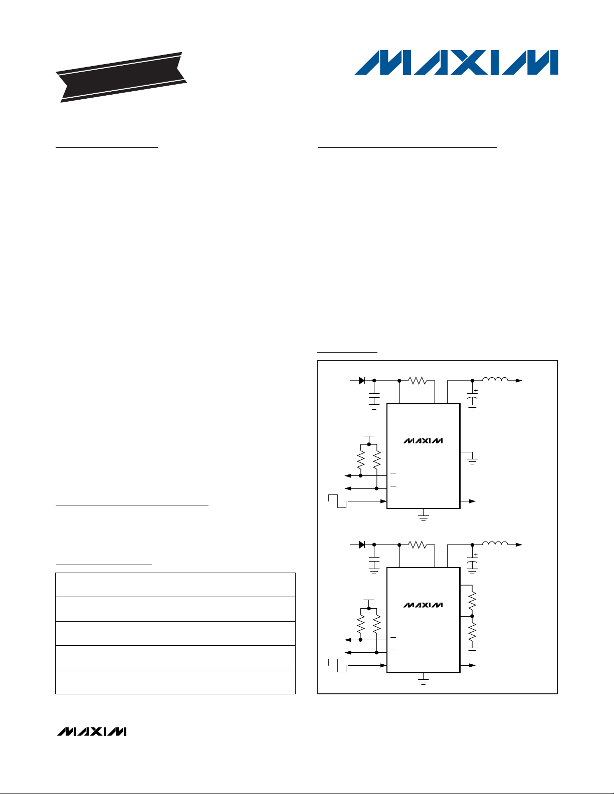
Typical Operating Circuits
MAX16913
SC
OL
GND
OLT
IN
SHDN
SENS
BATTERY
INPUT
AOUT
TO ADC INPUT
OUT
TO
PROTECTED
LOAD (LNA)
3.3V TO 5V
MAX16913A
REF
REF
SC
OL
GND
OLT
IN
SHDN
SENS
BATTERY
INPUT
AOUT
TO ADC INPUT
OUT
TO
PROTECTED
LOAD (LNA)
3.3V TO 5V
PA R T
M A X1 6 9 1 3 G E E +
M AX 16913GE E /V + *
M A X1 6 9 1 3 A G E E +
M AX 16913AG E E /V + *
T EM P
R A N G E
- 40°C to
+ 105° C
- 40°C to
+ 105° C
- 40°C to
+ 105° C
- 40°C to
+ 105° C
PIN -
PA C K A G E
16 QS OP Inter nal l y S et
16 QS OP Inter nal l y S et
16 QS OP
16 QS OP
O PEN - L O A D
T H R ESH O L D
E xter nal l y
Ad j ustab l e
E xter nal l y
Ad j ustab l e
Page 2

MAX16913/MAX16913A
Remote Antenna Current-Sense
Amplifier and Switches
2 _______________________________________________________________________________________
ABSOLUTE MAXIMUM RATINGS
ELECTRICAL CHARACTERISTICS
(VIN= +9V to +18V, TA= TJ= T
MIN
to T
MAX
, unless otherwise noted. Typical values are at TA= +25°C.)
Stresses beyond those listed under “Absolute Maximum Ratings” may cause permanent damage to the device. These are stress ratings only, and functional
operation of the device at these or any other conditions beyond those indicated in the operational sections of the specifications is not implied. Exposure to
absolute maximum rating conditions for extended periods may affect device reliability.
IN to GND ............................................….…………-0.3V to +42V
OUT to GND ...........................................................-0.3V to +42V
SENS to IN.............................................................-0.3V to +0.3V
SC, OL, SHDN, OLT, AOUT to GND..................…-0.3V to +6.0V
Current into Any Pin Except OUT and SENS....................±20mA
Current into SENS and OUT ...........................................±340mA
Continuous Power Dissipation (T
A
= +70°C)
16-Pin QSOP (derate 18.2mW/°C above +70°C)....1454.5mW
Junction-to-Case Thermal Resistance (θ
JC
) (Note 1) ......25°C/W
Junction-to-Ambient Thermal Resistance (θ
JA
) (Note 1) .....55°C/W
Operating Temperature Range .........................-40°C to +105°C
Junction Temperature........................................-40°C to +150°C
Storage Temperature Range .............................-65°C to +150°C
Lead Temperature (soldering, 10s) .................................+300°C
Note 1: Package thermal resistances were obtained using the method described in JEDEC specification JESD51-7, using a four-layer
board. For detailed information on package thermal considerations, refer to www.maxim-ic.com/thermal-tutorial
.
PARAMETER SYMBOL CONDITIONS MIN TYP MAX UNITS
GENERAL
Operating Input Voltage Range V
Quiescent Supply Current I
Shutdown Supply Current I
(VIN - V
SENS
) to V
Gain Av V
AOUT
AOUT Maximum Voltage (VIN - V
AOUT Zero-Current Output Voltage (VIN - V
AOUT Voltage
AOUT Output Impedance Z
Switch Dropout Voltage V
Thermal Shutdown Threshold T
Thermal Shutdown Hysteresis T
Reference Output Voltage V
Reference Output Impedance Z
THRESHOLDS
Open-Load Current Threshold I
Nominal Open-Load Threshold
Setting Range
Short-Circuit Voltage Threshold V
Voltage between IN and SENS V
Overvoltage Shutdown Threshold V
Overcurrent Blanking Time t
Retry Time t
IN
V
CC
SD
AOUT
D
SHDN
HYST
REF
REF
OL
V
OLR
SC
LIM
OVLOVIN
BLANK
RETRY
< 0.4V 0.6 1.2 mA
SHDN
V
> 1.7V, TA = +25°C 5 µA
SHDN
/(VIN - V
AOUT
SENS
SENS
I
= ISC, (VIN - V
LOAD
I
= 2 x ISC, (VIN - V
LOAD
) 13 V/V
SENS
) > 300mV 4.3 V
) = 0 340 400 460 mV
) = 100mV 1.5 1.7 1.9
SENS
) = 200mV 2.7 3 3.3
SENS
Measured between SENS and OUT while
sourcing 100mA
Temperature rising +150 +164 °C
R
SENSE
= 1Ω (V
= 0.66V for the
OLT
MAX16913 only)
(MAX16913A only) 10 50 mV
R
= 1Ω 87 100 110 mV
SENSE
At current limit, VIN = 14V 173 200 225 mV
rising 18 21 24 V
518V
2.7 3 3.3 V
10 20 30 mA
100 200 ms
1500 3000 ms
5kΩ
0.6 V
15 °C
5kΩ
V
Page 3
MAX16913/MAX16913A
Remote Antenna Current-Sense
Amplifier and Switches
_______________________________________________________________________________________ 3
ELECTRICAL CHARACTERISTICS (continued)
(VIN= +9V to +18V, TA= TJ= T
MIN
to T
MAX
, unless otherwise noted. Typical values are at TA= +25°C.)
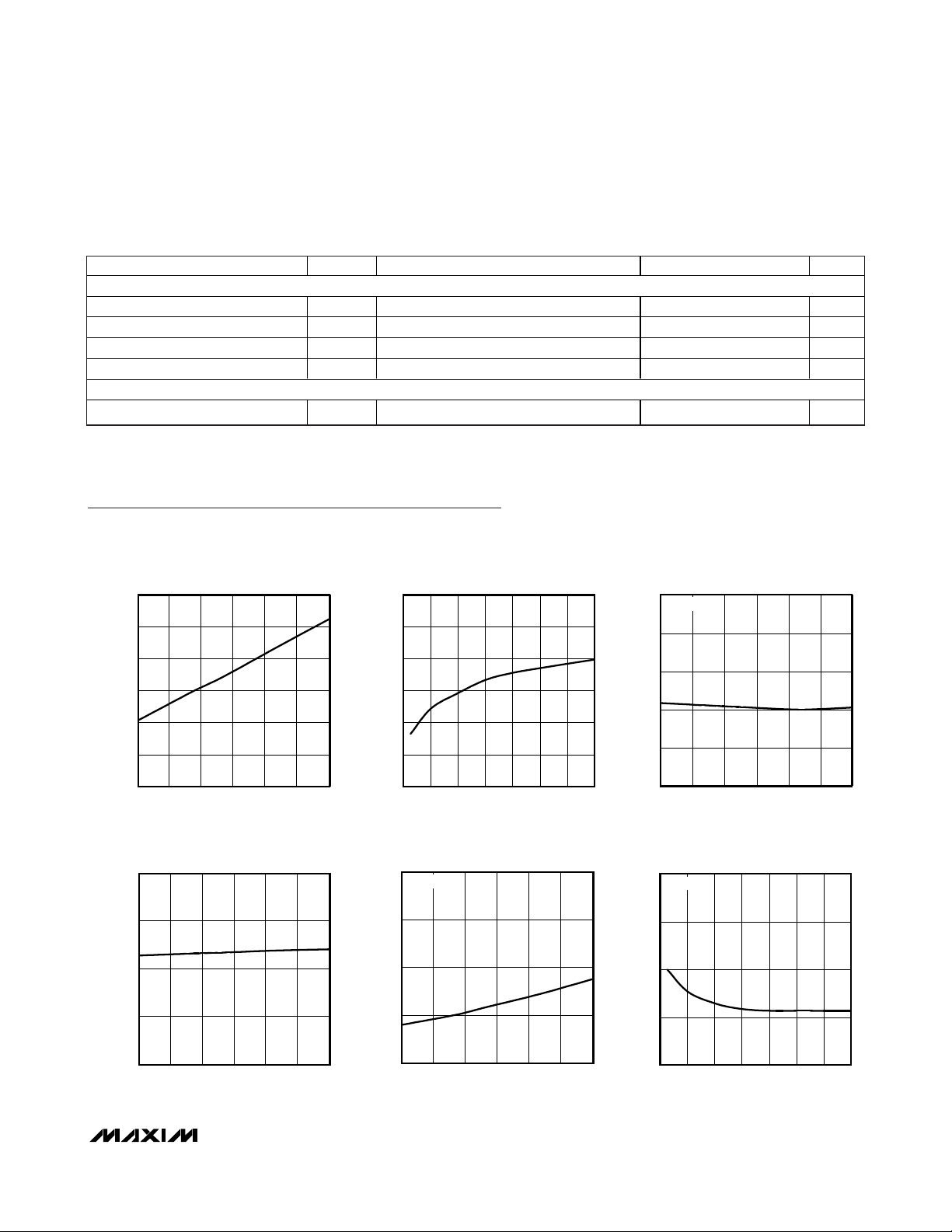
Typical Operating Characteristics
(VIN= 14V, R
SENSE
= 1Ω, TA= +25°C, unless otherwise noted.)
400
500
450
600
550
650
700
OPERATING SUPPLY CURRENT
vs. TEMPERATURE
TEMPERATURE (°C)
I
CC
(μA)
-40 10 35-15 60 85 105
MAX16913/3A toc01
200
400
300
600
500
700
800
410126 8 14 16 18
OPERATING SUPPLY CURRENT
vs. SUPPLY VOLTAGE
MAX16913/3A toc02
VIN (V)
I
CC
(μA)
0
1
3
2
4
5
-40 10-15 356085105
SHUTDOWN SUPPLY CURRENT
vs. TEMPERATURE
MAX16913/3A toc03
TEMPERATURE (°C)
I
SD
(μA)
VIN = 14V
14.0
13.5
13.0
12.5
12.0
-40 35-15 10 60 85 105
AOUT GAIN
vs. TEMPERATURE
MAX16913/3A toc04
TEMPERATURE (°C)
A
V
(V/V)
0.8
0.6
0.4
0.2
0
-40 35-15 10 60 85 105
(V
SENSE
- V
OUT
)
vs. TEMPERATURE
MAX16913/3A toc04
TEMPERATURE (°C)
V
SENSE
- V
OUT
(V)
I
OUT
= 90mA
0
0.2
0.4
0.6
0.8
(V
SENSE
- V
OUT
)
vs. V
IN
MAX16913/3A toc06
VIN (V)
V
SENSE
- V
OUT
(V)
410126 8 14 16 18
I
OUT
= 90mA
PARAMETER SYMBOL CONDITIONS MIN TYP MAX UNITS
LOGIC LEVELS
SC, OL Output-Voltage Low V
SC, OL Output-Leakage Current I
SHDN Input Low Voltage V
SHDN Input High Voltage V
TIMING
Startup Response Time t
Sink current = 1mA 0.4 V
OL
V
LEAK
IL
IH
ST
= VOL = 5V 0.01 µA
SC
SHDN falling edge to 90% of VIN, no load 100 µs
0.4 V
1.7 V
Page 4

MAX16913/MAX16913A
Remote Antenna Current-Sense
Amplifier and Switches
4 _______________________________________________________________________________________
Typical Operating Characteristics (continued)
(VIN= 14V, R
SENSE
= 1Ω, TA= +25°C, unless otherwise noted.)
OVERCURRENT SHUTDOWN
MAX16913/3A toc10
400ms/div
SHDN
I
OUT
5V/div
5V/div
100mA/div
SC
TOTAL CURRENT MEASUREMENT ERROR
- V
vs. (V
VIN - V
IN
SENSE
4
3
2
1
0
TOTAL CURRENT MEASUREMENT ERROR (%)
-1
10 40 5020 30 60 70 80 90 100
SENSE
(mV)
)
MAX16913/3A toc07
(ms)
t
BLANK
OVERCURRENT BLANKING TIME
300
250
200
150
100
50
0
-40 10 35-15 60 85 105
vs. TEMPERATURE
TEMPERATURE (°C)
SHDN
OVERCURRENT BLANKING TIME
300
250
MAX16913/3A toc08
200
(ms)
150
BLANK
t
100
50
0
410126 8 14 16 18
TURN-ON INTO CAPACITIVE LOAD
(OUTPUT STAYS ON) (C
LOAD
= 1000µF)
MAX16913/3A toc11
vs. V
VIN (V)
5V/div
IN
MAX16913/3A toc09
100mA/div
I
OUT
20ms/div
CURRENT-LIMIT VOLTAGE
vs. V
250
200
150
(mV)
SENSE
- V
100
IN
V
50
0
486 1012141618
IN
MAX16913/3A toc12
VIN (V)
Page 5

MAX16913/MAX16913A
Remote Antenna Current-Sense
Amplifier and Switches
_______________________________________________________________________________________ 5
Pin Description
MAX16913 Functional Diagram
OLT
REF
AOUT
FET
DRIVER AND
CONTROL
REF
OT
OUT
CURRENT
SENSE
SENS
IN
SHDN
CHARGE
PUMP
MAX16913A
GND
OL
SC
V
REF2
V
REF
MAX16913A Functional Diagram
PIN NAME FUNCTION
1, 8, 9, 16 GND Ground
2 IN Input Voltage. Bypass IN to GND with a low-ESR ceramic capacitor with a minimum value of 0.1µF.
3, 4 SENS Input to Current-Sense Amplifier. Connect the sense resistor between SENS and IN.
5, 6 OUT Switch Output
7 SHDN Active-High Control Input. Drive SHDN low to turn on the device.
10 N.C. No Connection. Not internally connected.
11 OLT
12 REF
13 AOUT
14 OL
15 SC
Open-Load Threshold Setting Input. A resistive divider between REF, OLT, and GND sets the open-load
current threshold (MAX16913A). For the MAX16913, connect OLT to GND.
+3V Nominal Reference Output. Use a resistive divider between REF, OLT, and ground to set the open-load
current threshold (MAX16913A). The output impedance of this voltage regulator is 5kΩ.
Current-Monitor Voltage Output. AOUT can be used to measure the load current by means of an external
ADC. The output impedance is 5kΩ.
Open-Drain Open-Load Indicator Output. OL goes low when the load current is lower than the open-load
current threshold, or when there is a short-to-battery fault. Connect OL to a 10kΩ pullup resistor. See Table 1.
Open-Drain Short-Circuit Indicator Output. SC goes low when the load current is greater than the short-circuit
current threshold or when there is a short-to-battery fault. Connect SC to a 10kΩ pullup resistor. See Table 1.
SENS
IN
SHDN
SC
OL
MAX16913
CURRENT
SENSE
CHARGE
OLT
PUMP
OT
REF
GND
FET
DRIVER AND
CONTROL
V
REF
V
REF2
OUT
AOUT
REF
Page 6

MAX16913/MAX16913A
Remote Antenna Current-Sense
Amplifier and Switches
6 _______________________________________________________________________________________
Detailed Description
The MAX16913/MAX16913A high-voltage, high-side,
current-sense switches feature internal current limiting
to prevent system damage due to fault conditions. The
MAX16913/MAX16913A input voltage range extends
from 5V to 18V, making them ideal for providing phantom power to remote radio-frequency low-noise amplifiers (LNAs) in automotive applications. High-side
current monitoring does not interfere with the ground
path of the load being measured, making these
devices particularly useful in a wide range of high-voltage battery-powered systems.
The MAX16913/MAX16913A monitor the load current
by means of a high-side current-sense amplifier and
provide an analog output voltage proportional to that
current at AOUT.
The devices combine a high-side current-sense amplifier, an internal switch, a +3V bandgap reference, and
two open-drain fault indicator outputs. These features
enable the design of remote power circuits with shortcircuit, short-to-battery, and thermal protection. For the
MAX16913A, the open-load threshold is externally
adjustable using a resistive divider.
A fault-blanking feature enables the circuit to ignore
momentary faults, such as those caused by initial
charging of a capacitive load at turn-on, preventing
false alarms to the system.
The MAX16913/MAX16913A provide an active-high
control input (SHDN) to put the devices in low-power
shutdown mode.
Current-Sense Amplifier
The integrated current-sense amplifier is a differential
amplifier that amplifies the voltage between VINand
V
SENS
. A sense resistor (0.65Ωmin, 4.7Ωmax), R
SENSE
,
is connected across VINand V
SENS
. When the load
current passes through the sense resistor, a voltage
drop develops across it. The current-sense amplifier
amplifies this voltage.
The current-sense amplifier features an internally fixed
gain of 13V/V (typ). The following equations show the
relationship between the current-sense amplifier output
voltage (AOUT) and load current:
AOUT is the output of an internal buffer with a 5kΩ output impedance.
The AOUT voltage is clamped to typically 4.3V in order
to avoid damage to external circuitry.
Load Protection
The MAX16913/MAX16913A monitor the load current
through an external sense resistor and perform the following actions:
• If the monitored current is lower than the open-load
current, the device signals open load (see the
Open Load
section).
• If the monitored current is higher than the short-circuit current (ISC), the device enters the short-circuit
mode (see the
Short Circuit
section).
The devices also perform a short-to-battery detection
every time the internal switch turns on (see the
Short-to-
Battery Detection
section). In addition, thermal shutdown protects the MAX16913/MAX16913A from
overheating (see the
Thermal Shutdown
section). Two
open-drain outputs (OL and SC) indicate the device
status (see Table 1).
Open Load
If the load current drops below the open-load current
threshold, the OL output asserts low. An open-load
condition does not turn off the internal switch. The
MAX16913 provides an internally fixed open-load
threshold, while the MAX16913A features an adjustable
open-load threshold.
For the MAX16913, when (VIN- V
SENS
) drops below
20mV (typ), the device signals open load.
For the MAX16913A, using a resistive divider between
REF, the open-load threshold adjustment pin (OLT),
and GND sets the open-load threshold (see the
Open-
Load Threshold Selection
section).
Short Circuit
If the load current reaches the short-circuit current
threshold (ISC), the t
BLANK
timer begins counting.
During this period, the load current is limited to a value
of twice the short-circuit current threshold (2 x ISC). If
the short-circuit condition is present for t
BLANK
, SC
asserts low and the internal switch turns off. The timer
resets if the short-circuit condition disappears before
the blanking time (t
BLANK
) has elapsed. If the switch is
turned off at the end of t
BLANK
, a retry timer (t
RETRY
)
starts immediately after the blanking time has elapsed.
During that time, the switch stays off. At the end of
t
RETRY
, the switch turns on again. If the fault still exists,
the cycle repeats. If the fault has been removed, the
switch stays on. During this cycle, SC stays low. During
retry when the switch is off, the current through the
(V -V )(V)
I A
()==×
V V A (V/V) (V -V )(V) + 0.4V
AOUT V IN SENS
()
LOAD
[]
IN SENS
R
SENSE
()
Ω
Page 7

MAX16913/MAX16913A
Remote Antenna Current-Sense
Amplifier and Switches
_______________________________________________________________________________________ 7
switch is zero (see Figure 1). If the load current is
greater than ISC, but does not reach the 2 x ISCthreshold, the t
BLANK
timer still begins counting (see Figure
2). The resistor across IN and SENS sets ISCto a typical value of 100mV/R
SENSE
(Ω). Blanking time and retry
time have fixed values of 100ms (min) and 1500ms
(min), respectively.
Short-to-Battery Detection
It may happen that OUT is shorted to the battery due to
a fault in the system. The MAX16913/MAX16913A
detect this failure by comparing the OUT voltage and
the IN voltage before the switch turns on. Every time
the switch turns on, such as at the end of the retry time,
or once the thermal shutdown condition disappears,
the short-to-battery detection is performed. At this
point, if the device detects any failure, the switch stays
off, and both SC and OL assert low (see Table 1).
Thermal Shutdown
Thermal shutdown circuitry protects the devices from
overheating. The switch turns off immediately when the
junction temperature exceeds +150°C (min) (see Table
1). The switch turns on again after the device temperature drops by approximately 15°C (typ).
Shutdown (SHDN)
The MAX16913/MAX16913A feature an active-high control input (SHDN) to put the devices in a low-power shutdown mode. The devices turn off and consume only 5µA
(max) of shutdown current when SHDN is driven high.
Figure 1. Short-Circuit Timing Diagram
2 x I
LOAD CURRENT
SHDN
2 x I
LOAD CURRENT
TURN-ON INTO A HARD SHORT CIRCUIT
SC
I
SC
t
BLANK
SC
TURN-ON INTO A TEMPORARY SHORT CIRCUIT
SC
I
SC
t
BLANK
t
RETRY
t
RETRY
RETRY
SHDN
SC
RETRY
Page 8

MAX16913/MAX16913A
Remote Antenna Current-Sense
Amplifier and Switches
8 _______________________________________________________________________________________
Undervoltage and Overvoltage Lockout
The MAX16913/MAX16913A include undervoltage circuitry (UVLO) to prevent erroneous switch operation
when the input voltage goes below approximately
4.25V during startup and brownout conditions. Input
voltages of less than 4.25V inhibit operation of the
device by turning off the internal charge pump and the
switch. These devices also feature an overvoltage lockout (OVLO) threshold of +21V (typ). When VINis
greater than V
OVLO
, the device immediately turns off
the switch and the internal charge pump.
Internal Reference
The MAX16913/MAX16913A feature a +3V bandgap
reference output, stable over supply voltage and temperature. For the MAX16913A, the reference output is
connected to the resistive divider which sets the openload threshold. The output impedance of the internal
reference is 5kΩ (typ).
Figure 2. Overcurrent Timing Diagram
Table 1. Status Truth Table
TURN-ON WITH A HEAVY LOAD
2 x I
SC
I
SC
LOAD CURRENT
t
BLANK
t
RETRY
SHDN
SC
TURN-ON INTO A TEMPORARY HEAVY LOAD
2 x I
SC
LOAD CURRENT
SHDN
I
SC
t
BLANK
SC
t
RETRY
RETRY
RETRY
SC OL V
AOUT
0 0 0.4V OUT Short-to-Battery
01C ycl i ng Whi l e Autor etr yi ng Short-Circuit Condition
1 0 0.4V Open-Load Condition
11(VIN - V
) x 13 + 0.4V Normal Operation
SENS
DEVICE STATUS
Page 9

MAX16913/MAX16913A
Remote Antenna Current-Sense
Amplifier and Switches
_______________________________________________________________________________________ 9
Applications Information
Choosing the Sense Resistor
Ideally, the maximum load current develops the fullscale sense voltage across the current-sense resistor.
The current-sense amplifier output voltage is given by:
V
AOUT
(V) = [(VIN- V
SENS
)(V) x AV(V/V)] + 0.4(V)
where V
AOUT
is the output voltage of the current-sense
amplifier, and AVis the gain of the current-sense amplifier
of 13V/V (typ). Calculate the maximum value for R
SENSE
so that the differential voltage across IN and SENS does
not exceed the minimum full-scale sense voltage (87mV):
where V
DIFF(MIN)
= V
IN
- V
SENS
= 87mV minimum at
maximum load current.
Use resistors specified for current-sensing applications
with a minimum resistance value of 0.65Ω, and the
maximum resistance value of 4.7Ω. Keep inductance
low if I
SENSE
has a large high-frequency component.
Wire-wound resistors have the highest inductance,
while metal film is somewhat better. Low-inductance
metal-film resistors are also available. Instead of being
spiral wrapped around a core, as in metal-film or wirewound resistors, they are a straight band of metal and
are available in values under 1Ω. Because of the high
current that flows through R
SENSE
, avoid parasitic trace
resistance from causing errors in the sense voltage.
Open-Load Threshold Selection
For the MAX16913A, a resistive divider between REF,
OLT, and GND sets the open-load threshold. See
Figure 3.
Use the following formula to set the desired open-load
threshold:
where IOLis the desired open-load current threshold;
A
V
is the current-sense amplifier gain (13V/V typ), and
V
REF
is the reference voltage (+3V typ). The sum of R
1
and R2should be large enough so that the output
impedance of the internal reference (5kΩ) is negligible
compared to the sum of R1and R2, and has a minimum
effect on the accuracy of the adjusted open-load
threshold.
For example, to set the open-load threshold at 10mA,
using a 1Ω sense resistor, use the following method to
calculate the value of R
1
and R2:
Choose R1 = 470kΩ and calculate R2as 101kΩ.
Input Capacitor
Connect a low-leakage ceramic capacitor from IN to
GND to limit the input voltage drop during momentary
output short-circuit conditions, and to protect the
device against transients due to inductance in the IN
line. For example, use at least a 0.1µF ceramic capacitor if the input inductance (including any stray inductance) is estimated to be 20µH. Larger capacitor values
reduce the voltage undershoot at the input.
Output Capacitor
In an analogous fashion to the input capacitor, an output capacitor protects the device against transients
due to any series inductance in the output. Under no
conditions should the OUT pin voltage go below -0.3V
as specified in the
Absolute Maximum Ratings
. If a
capacitor alone is not sufficient to avoid large negative
transients on OUT, then a Schottky diode should be
used to clamp transients which go below ground. With
a 100µH output series inductor, a 220µF output capacitor is needed to eliminate potential problems. With larger inductor values or smaller capacitors, a Schottky
clamp diode will be necessary.
Layout and Thermal Dissipation
To optimize the switch response time to output shortcircuit condition, it is very important to keep all traces
as short as possible to reduce the effect of undesirable
parasitic inductance. Place input and output capacitors
as close as possible to the device (no more than 5mm).
Figure 3. Open-Load Threshold Selection
(R +R )(k )
R
SENSE
()Ω=
V (V)
DIFF
(MIN)
I (A)
LOAD
(FULL-SCALE)
R(k )
Ω
2
12
(R I (V/V))+ 0.4V
SENSE OL V
Ω
Ω=××() ()AA
V (V)
REF
REF
MAX16913
OLT
R
R
R(k )
Ω
2
(R +R )(k )
12
(1 (V/V))+ 0.4V
Ω
Ω=××
() . ()001 13A
3(V)
1
2
0.177
=
Page 10

MAX16913/MAX16913A
Remote Antenna Current-Sense
Amplifier and Switches
Maxim cannot assume responsibility for use of any circuitry other than circuitry entirely embodied in a Maxim product. No circuit patent licenses are
implied. Maxim reserves the right to change the circuitry and specifications without notice at any time.
10
____________________Maxim Integrated Products, 120 San Gabriel Drive, Sunnyvale, CA 94086 408-737-7600
© 2008 Maxim Integrated Products is a registered trademark of Maxim Integrated Products, Inc.
SPRINGER
IN and OUT must be connected with wide short traces
to the power bus. During normal operation, the power
dissipation is small and the package temperature
change is minimal. If the output is continuously shorted
to ground at the maximum supply voltage, the devices
are protected because the total power dissipated dur-
ing the short is scaled down by the duty cycle imposed
by the protection:
Package Information
For the latest package outline information, go to
www.maxim-ic.com/packages
.
PACKAGE TYPE PACKAGE CODE DOCUMENT NO.
16 QSOP E16-8F
21-0112
Chip Information
PROCESS: BiCMOS
Pin Configuration
16
15
14
13
12
11
10
9
1
2
3
4
5
6
7
8
GND
GND
AOUT
REF
OLT
N.C.
GND
TOP VIEW
MAX16913
MAX16913A
QSOP
SC
OL
IN
SENS
OUT
SENS
OUT
SHDN
GND
+
Maxim cannot assume responsibility for use of any circuitry other than circuitry entirely embodied in a Maxim product. No circuit patent licenses are
implied. Maxim reserves the right to change the circuitry and specifications without notice at any time.
10
____________________Maxim Integrated Products, 120 San Gabriel Drive, Sunnyvale, CA 94086 408-737-7600
© 2008 Maxim Integrated Products is a registered trademark of Maxim Integrated Products, Inc.
P
(MAX)
VI t
IN
=
××
(MAX)
OUT
(MAX)
t+t
RETRY BLANK
BLANK
 Loading...