

Page 1
19-4816; Rev 0; 7/09
200mA, Automotive, Ultra-Low
Quiescent Current, Linear Regulator
General Description
The MAX16910 ultra-low quiescent current, high-voltage
linear regulator is ideal for use in automotive and batteryoperated systems. The device operates from a +3.5V to
+30V input voltage, delivers up to 200mA of load current, and consumes only 20µA of quiescent current at
no load. The device consumes only 1.6µA current when
in shutdown. The input is +45V transient tolerant and is
designed to operate under load-dump conditions. The
MAX16910 can be configured as either fixed output voltage (+3.3V or +5V) or adjustable output voltage using an
external resistive divider.
The MAX16910 features an open-drain, active-low RESET
output with fixed thresholds offered at 92.5% and 87.5%
of the output voltage. The RESET output remains low for
a fixed period of 60µs after the output voltage exceeds
its threshold. The RESET delay can be extended with an
external capacitor.
The MAX16910 includes an enable input, short-circuit
protection, and thermal shutdown. The MAX16910 operates over the -40°C to +125°C automotive temperature
range. The device is available in a space-saving, thermally enhanced, 3mm x 3mm, 8-pin TDFN package and
5mm x 4mm, 8-pin SO package.
MAX16910
Features
S Low 20µA Quiescent Current
S +3.5V to +30V Wide Input Voltage Range, +45V
Tolerant
S Operates Through Cold-Crank Conditions
S Low-Dropout Voltage of 280mV at 200mA
S Up to 200mA Output Current Capability
S Stable Operation with Tiny 4.7µF Output Capacitor
S User-Selectable Output Voltage
+3.3V or +5V Fixed
+1.5V to +11V Adjustable with External
Resistive Divider
S Open-Drain RESET Output with Adjustable Delay
S Fixed-Reset Threshold Options: 87.5% or 92.5%
S High-Voltage Enable Input (+45V)
S Thermal and Short-Circuit Protection
S Operating -40°C to +125°C Temperature Range
S Automotive Qualified
Applications
Automotive
Industrial
Telecom
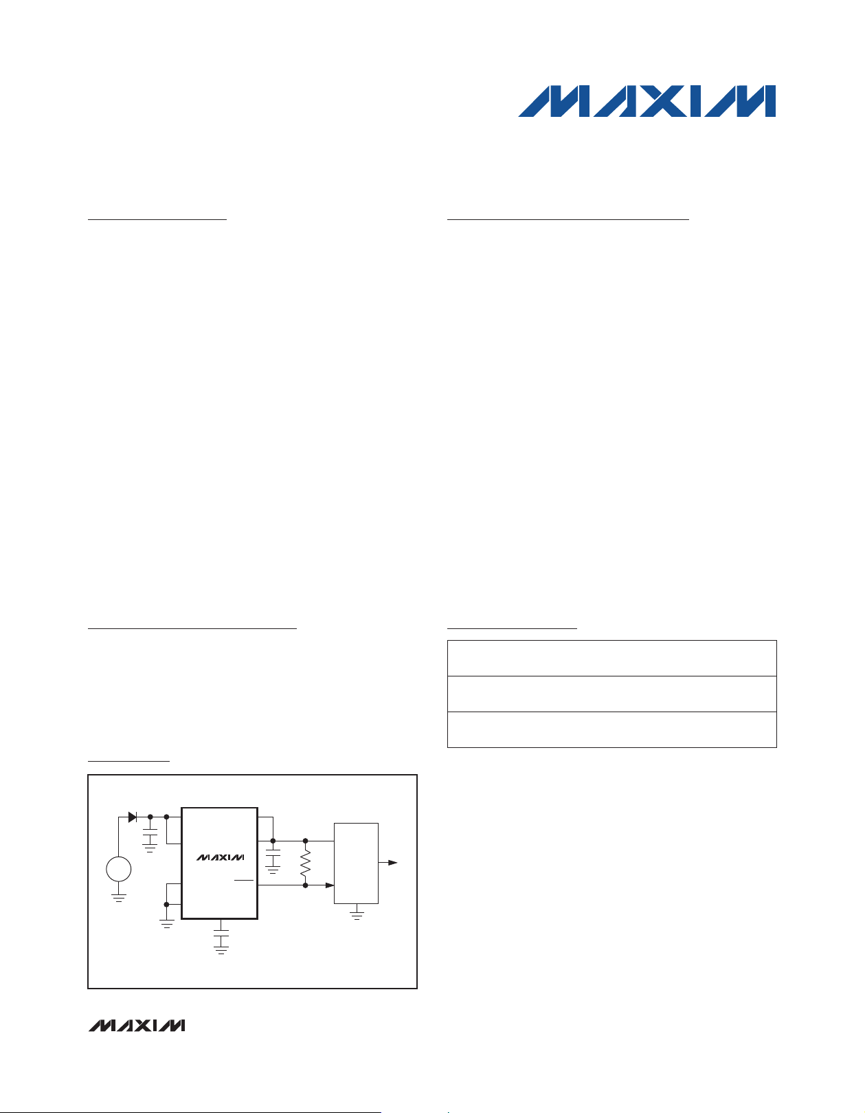
Typical Operating Circuits
5V FIXED OUTPUT
IN
1µF
+
14V
BATTERY
-
Typical Operating Circuits continued on next page.
ENABLE
SET
GND
MAX16910
TIMEOUT
OUT
SETOV
RESET
1nF
(1.25ms DELAY)
4.7µF
10kI
V
CC
RESET
µC
I/O
Ordering Information
I
PART
MAX16910CATA_/V+ 200
MAX16910CASA_/V+ 200
Insert the desired suffix numbers (from the Selector Guide) into
the blank “_” to indicate reset threshold.
+Denotes a lead(Pb)-free/RoHS-compliant package.
/V Denotes an automotive qualified part.
*EP = Exposed pad.
OUT
(mA)
TEMP
RANGE
-40NC to
+125NC
-40NC to
+125NC
PINPACKAGE
8 TDFN-EP*
(3mm x 3mm)
8 SO-EP*
(5mm x 4mm)
_______________________________________________________________ Maxim Integrated Products 1
For pricing, delivery, and ordering information, please contact Maxim Direct at 1-888-629-4642,
or visit Maxim’s website at www.maxim-ic.com.
Page 2
200mA, Automotive, Ultra-Low
Typical Operating Circuits (continued)
Quiescent Current, Linear Regulator
3.3V FIXED OUTPUT
MAX16910
IN
1µF
+
14V
BATTERY
-
1µF
+
14V
BATTERY
-
ENABLE
SET
GND
ADJUSTABLE OUTPUT
IN
ENABLE
SET
GND
MAX16910
TIMEOUT
MAX16910
TIMEOUT
SETOV
RESET
1nF
(1.25ms DELAY)
OUT
SETOV
RESET
1nF
(1.25ms DELAY)
OUT
4.7µF
R1
R2
4.7µF
V
10kI
RESET
V
10kI
RESET
CC
µC
CC
µC
I/O
I/O
2 ______________________________________________________________________________________
Page 3
200mA, Automotive, Ultra-Low
Quiescent Current, Linear Regulator
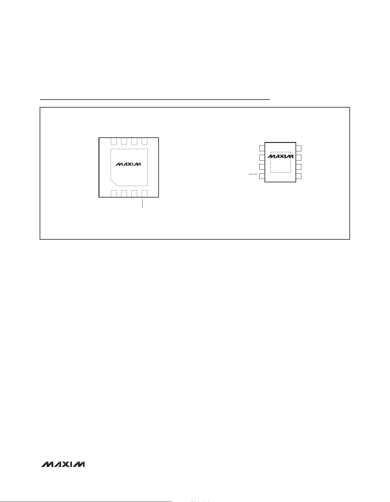
Pin Configurations
TOP VIEW
OUT
8172635
MAX16910
+
IN
*CONNECT EXPOSED PAD TO GND.
GND
ENABLE
TDFN
SETOV
SET
TIMEOUT
*EP
4
RESET
TOP VIEW
+
1
IN
2
MAX16910
3
SET
RESET
4
*CONNECT EXPOSED PAD TO GND.
*EP
SO
87OUT
GNDENABLE
SETOV
6
TIMEOUT
5
MAX16910
_______________________________________________________________________________________ 3
Page 4
200mA, Automotive, Ultra-Low
Quiescent Current, Linear Regulator
ABSOLUTE MAXIMUM RATINGS
(All voltages referenced to GND.)
IN, ENABLE, SET.................................................. -0.3V to +45V
OUT, RESET (open-drain output)............................-0.3V to +12V
SETOV, TIMEOUT....................................................-0.3V to +6V
Maximum Current (all pins except IN and OUT)...............50mA
Continuous Power Dissipation (TA = +70°C)
8-Pin TDFN (derate 24.4mW/°C above +70°C)*.............1951mW
8-Pin SO (derate 23.3mW/°C above +70°C)*................1861mW
MAX16910
*As per JEDEC51 Standard (multilayer board).
Note 1: Package thermal resistances were obtained using the method described in JEDEC specification JESD51-7, using a four-layer
board. For detailed information on package thermal considerations, refer to www.maxim-ic.com/thermal-tutorial.
Stresses beyond those listed under “Absolute Maximum Ratings” may cause permanent damage to the device. These are stress ratings only, and functional operation of the device at these
or any other conditions beyond those indicated in the operational sections of the specifications is not implied. Exposure to absolute maximum rating conditions for extended periods may
affect device reliability.
ELECTRICAL CHARACTERISTICS
(VIN = V
otherwise noted. Typical values are TA = +25°C.) (Note 2)
ENABLE
= +14V, C
TIMEOUT
= open, CIN = 1µF, C
OUT
Junction-to-Case Thermal Resistance (ΘJC) (Note 1)
8-Pin TDFN.......................................................................8°C/W
8-Pin SO...........................................................................7°C/W
Junction-to-Ambient Thermal Resistance (ΘJA) (Note 1)
8-Pin TDFN.....................................................................41°C/W
8-Pin SO.........................................................................43°C/W
Operating Temperature Range..........................-40°C to +125°C
Junction Temperature......................................................+150°C
Storage Temperature Range..............................-65°C to +150°C
Lead Temperature (soldering, 10s).................................+300°C
= 4.7µF, unless otherwise noted. TA = TJ = -40°C to +125°C, unless
PARAMETER SYMBOL CONDITIONS MIN TYP MAX UNITS
Supply Voltage Range V
Supply Current I
Shutdown Supply Current I
Output Voltage
(5V Fixed Output Setting)
Output Voltage
(3.3V Fixed Output Setting)
Adjustable Output-Voltage Range V
SETOV FB Voltage V
Dropout Voltage (Note 4) DV
Short-Circuit Output Current Limit I
Thermal Shutdown (Note 5) +180 NC
SHDN
V
OUT50
V
OUT33
OUT
SETOVILOAD
SC
Continuous 3.5 30
IN
For P 400ms 45
= 0, SET = GND, V
LOAD
ENABLE = GND, TA = +25NC 1.6 3
ENABLE = GND, -40NC P TA P +125NC 3
1mA P I
VIN = 6V to 30V (Note 3)
1mA P I
(Note 3)
I
LOAD
DO
HIGH, V
Output shorted to GND (MAX16910C__) 230 330 mA
P 200mA,
LOAD
P 200mA, VIN = 4.8V to 30V
LOAD
= 1mA 1.225 1.25 1.275 V
= 200mA, SET = GND, SETOV =
OUT(NORM)
= +5.0V
= 5V 20 30 FA
OUT
4.9 5.0 5.1 V
3.234 3.3 3.366 V
1.5 11.0 V
280 600 mV
FA
V
4 ______________________________________________________________________________________
Page 5

200mA, Automotive, Ultra-Low
Quiescent Current, Linear Regulator
ELECTRICAL CHARACTERISTICS (continued)
(VIN = V
otherwise noted. Typical values are TA = +25°C.) (Note 2)
Thermal Shutdown Hysteresis (Note 5) +25 NC
Line Regulation
(5V Fixed Output Setting)
Line Regulation
(3.3V Fixed Output Setting)
Load Regulation
(5V Fixed Output Setting)
Load Regulation
(3.3V Fixed Output Setting)
Power-Supply Rejection Ratio PSRR
Startup Response Time t
TIMEOUT INPUT
TIMEOUT Ramp Current I
TIMEOUT Ramp Delay 1.25 ms/nF
RESET Default Timeout Period V
RESET OUTPUT
RESET Threshold
RESET Threshold Hysteresis V
OUT to RESET Delay V
RESET Output-Voltage Low
(Open-Drain)
RESET Open-Drain Leakage
Current
RESET Open-Drain Leakage
Current
ENABLE
ENABLE Logic-Low V
ENABLE Logic-High V
ENABLE Pulldown Current (Note 6) 0.65 FA
SET INPUT
SET Input Current (All Modes)
SET Logic-Low V
Set Logic-High V
= +14V, C
ENABLE
PARAMETER SYMBOL CONDITIONS MIN TYP MAX UNITS
TIMEOUT
= open, CIN = 1µF, C
VIN = 6V to 30V, I
VIN = 4.8V to 30V, I
I
= 1mA to 200mA 12 mV
LOAD
I
= 1mA to 200mA 12 mV
LOAD
I
= 10mA, f = 100Hz, 500mV
LOAD
(Note 5)
START
TO
V
ILSET
IHSET
Rising edge of VIN to V
(Note 5)
TIMEOUT connected to GND 0.600 1.0 1.650 FA
rising, TIMEOUT = OPEN 30 60 90 Fs
OUT
MAX16910__9/V+, V
MAX16910__8/V+, V
rising 5
OUT
falling (Note 5) 4 Fs
OUT
I
OL
IL
IH
= 0.5mA, RESET asserted 0.4 V
SINK
RESET not asserted, RESET = 7V,
TA = +25NC
RESET not asserted, RESET = 7V,
-40NC ≤ TA ≤ +125NC
TA = +25NC -50 +50 nA
TA = +125NC 0.2 FA
= 4.7µF, unless otherwise noted. TA = TJ = -40°C to +125°C, unless
OUT
= 1mA 1 mV
LOAD
= 1mA 1 mV
LOAD
P-P
, I
LOAD
= 50mA
2.4 V
2.4 V
OUT
falling 90 92.5 94
OUT
falling 85 87.5 89
OUT
60 dB
160 Fs
1 FA
0.03 FA
0.4 V
0.4 V
% of
V
OUT
% of
V
OUT
MAX16910
_______________________________________________________________________________________ 5
Page 6
200mA, Automotive, Ultra-Low
SUPPLY CURRENT
GROUND CURRENT
SHUTDOWN SUPPLY CURRENT
Quiescent Current, Linear Regulator
ELECTRICAL CHARACTERISTICS (continued)
(VIN = V
otherwise noted. Typical values are TA = +25°C.) (Note 2)
SETOV INPUT (TRI-MODE)
SETOV Input Leakage Current
SETOV Low-Level Input Voltage V
MAX16910
SETOV High-Level Input Voltage V
Note 2: Production tested at TA = +25°C. Overtemperature limits are guaranteed by design.
Note 3: Observe the absolute maximum power dissipation limits.
Note 4: Dropout voltage is defined as (VIN - V
Note 5: Not production tested.
Note 6: ENABLE is internally pulled to GND.
ENABLE
= +14V, C
TIMEOUT
= open, CIN = 1µF, C
= 4.7µF, unless otherwise noted. TA = TJ = -40°C to +125°C, unless
OUT
PARAMETER SYMBOL CONDITIONS MIN TYP MAX UNITS
ILSETOV
IHSETOV
SET = HIGH, V
or SET = GND, V
SET = GND, V
device in +3.3V fixed output-voltage mode
SET = GND, V
device in +5V fixed output-voltage mode
) when V
OUT
OUT
= 5V
SETOV
= 5V
SETOV
SETOV
SETOV
< V
> V
ILSETOV
IHSETOV
or places
or places
is 2% below the value of V
OUT
V
OUT
- 0.4
for VIN = V
1 FA
0.4 V
+ 3V.
OUT
V
Typical Operating Characteristics
(VIN = VEN = +14V, CIN = 1µF, C
vs. SUPPLY VOLTAGE
30
I
= 0
LOAD
27
24
(FA)
IN
I
21
18
15
0 30
VIN (V)
= 4.7µF ceramic, TA = +25°C, unless otherwise noted.)
OUT
vs. LOAD CURRENT
80
V
= 3.3V
OUT
MAX16910 toc01
60
(FA)
GND
I
252015105
TA = +125NC
40
20
0
0 200
I
(mA)
LOAD
TA = -40NC
TA = +25NC
18016014012010080604020
MAX16910 toc02
10
vs. SUPPLY VOLTAGE
8
6
(FA)
IN
I
4
2
0
0 30
VIN (V)
MAX16910 toc03
252015105
6 ______________________________________________________________________________________
Page 7

200mA, Automotive, Ultra-Low
SHUTDOWN SUPPLY CURRENT
I
(
A)
RESET THRESHOLD
DROPOUT VOLTAGE vs. LOAD CURRENT
DROPOUT VOLTAGE vs. LOAD CURRENT
DROPOUT VOLTAGE (V)
V
(V)
Quiescent Current, Linear Regulator
Typical Operating Characteristics (continued)
(VIN = VEN = +14V, CIN = 1µF, C
= 4.7µF ceramic, TA = +25°C, unless otherwise noted.)
OUT
MAX16910
10
8
6
F
IN
4
2
0
-50 150
VIN = 30V
VIN = 14V
VIN = 6V
TEMPERATURE (NC)
(3.3V OUTPUT)
vs. TEMPERATURE
0.50
0.45
0.40
0.35
0.30
0.25
0.20
0.15
0.10
0.05
0
TA = +25NC
TA = -40NC
0 200
TA = +150NC
TA = +125NC
LOAD CURRENT (mA)
5.5
V
= 5V
OUT
5.2
MAX16910 toc04
RESET THRESHOLD VOLTAGE (V)
1007550250-25
125
MAX16910_9/V RISING
4.9
4.6
4.3
4.0
-50 150
MAX16910_9/V FALLING
MAX16910_8/V RISING
MAX16910_8/V FALLING
1007550250-25
TEMPERATURE (NC)
125
0.50
0.45
MAX16910 toc05
0.40
0.35
0.30
0.25
0.20
0.15
DROPOUT VOLTAGE (V)
0.10
0.05
0
0 200
OUTPUT VOLTAGE vs.
SUPPLY VOLTAGE
vs. TEMPERATURE
MAX16910 toc08
(V)
OUT
V
5.5
5.0
4.5
4.0
3.5
3.0
2.5
2.0
1.5
1.0
0.5
0
0 40
3.5
3.0
MAX16910 toc07
2.5
2.0
(V)
OUT
V
1.5
1.0
0.5
180160120 14040 60 80 10020
0
0 40
VIN (V)
I
= 0
LOAD
SETOV = GND
SET = GND
3530252015105
(5V OUTPUT)
TA = +150NC
TA = +125NC
TA = +25NC
TA = -40NC
LOAD CURRENT (mA)
OUTPUT VOLTAGE vs.
SUPPLY VOLTAGE
VIN (V)
I
= 0
LOAD
SETOV = OUT
SET = GND
MAX16910 toc06
180160120 14040 60 80 10020
MAX16910 toc09
353020 2510 155
OUTPUT VOLTAGE vs.TEMPERATURE
5.05
I
LOAD
5.03
5.01
OUT
4.99
4.97
4.95
-50 125
POWER-SUPPLY REJECTION RATIO
vs. FREQUENCY
0
I
= 10mA
LOAD
V
= 14V + 0.5V
IN
-10
-20
-30
PSRR (dB)
-40
-50
-60
-70
0.01 1000
P-P
FREQUENCY (kHz)
= 64mA
TEMPERATURE (NC)
RESET TIMEOUT PERIOD vs.
TEMPERATURE
60
C
UNCONNECTED
TIMEOUT
55
MAX16910 toc10
50
45
40
35
TIMEOUT PERIOD (Fs)
30
25
20
1007550250-25
125
-50 150
TEMPERATURE (NC)
MAX16910 toc11
125100-25 0 25 50 75
_______________________________________________________________________________________ 7
MAX16910 toc12
1001010.1
Page 8

200mA, Automotive, Ultra-Low
LOAD-TRANSIENT RESPONSE
Quiescent Current, Linear Regulator
Typical Operating Characteristics (continued)
(VIN = VEN = +14V, CIN = 1µF, C
= 4.7µF ceramic, TA = +25°C, unless otherwise noted.)
OUT
RESET OUTPUT VOLTAGE
vs. SINK CURRENT
1.5
1.2
MAX16910
0.9
0.6
RESET OUTPUT VOLTAGE (V)
0.3
0
0.001 10
RESET SINK CURRENT (mA)
LOAD-TRANSIENT RESPONSE
(3V OUTPUT)
10.10.01
MAX16910 toc16
1000
MAX16910 toc13
100
TIMEOUT PERIOD (ms)
V
OUT
(AC-COUPLED)
100mV/div
180mA
I
OUT
10mA
RESET TIMEOUT PERIOD vs.
TIMEOUT CAPACITANCE
10
1
0.1
0.01 100
C
TIMEOUT
1010.1
(nF)
LINE-TRANSIENT RESPONSE
(5V OUTPUT)
MAX16910 toc17
MAX16910 toc14
V
OUT
(AC-COUPLED)
200mV/div
28V
V
IN
6V
(5V OUTPUT)
200Fs/div
MAX16910 toc15
LINE-TRANSIENT RESPONSE
(3.3V OUTPUT)
MAX16910 toc18
V
OUT
(AC-COUPLED)
100mV/div
180mA
I
OUT
10mA
V
OUT
(AC-COUPLED)
200mV/div
28V
V
IN
4.8V
200Fs/div
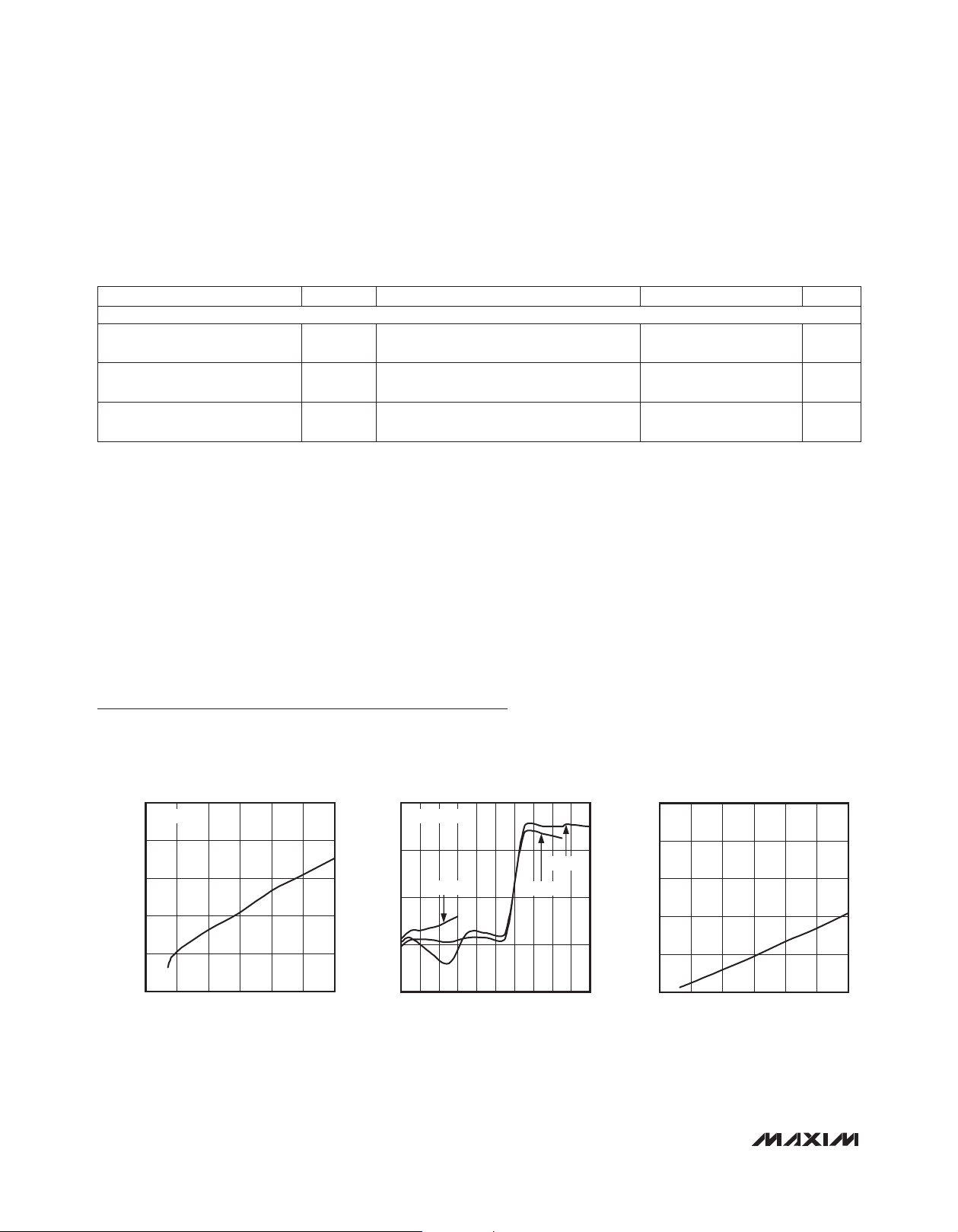
POWER-UP RESPONSE
40Fs/div
MAX16910 toc19
I
= 0A
OUT
VIN = V
EN
14V
V
IN
0V
3.3V
V
OUT
0V
2ms/div
POWER-UP RESPONSE
8 ______________________________________________________________________________________
40Fs/div
I
= 170mA
OUT
VEN = V
2ms/div
MAX16910 toc20
IN
14V
V
IN
0V
3.3V
V
OUT
0V
170mA
I
OUT
0A
Page 9

200mA, Automotive, Ultra-Low
Quiescent Current, Linear Regulator
Typical Operating Characteristics (continued)
(VIN = VEN = +14V, CIN = 1µF, C
= 4.7µF ceramic, TA = +25°C, unless otherwise noted.)
OUT
MAX16910
ENABLE STARTUP RESPONSE
40Fs/div
MAX16910 toc21
5V
V
0V
3.3V
V
0A
IN
OUT
ENABLE STARTUP RESPONSE
40Fs/div
MAX16910 toc22
5V
V
EN
0V
3.3V
V
OUT
0V
175mA
I
OUT
0A
LOAD-DUMP TRANSIENT RESPONSE
100ms/div
MAX16910 toc23
V
OUT
(AC-COUPLED)
100mV/div
42V
V
IN
14V
Pin Description
PIN NAME FUNCTION
1 IN Regulator Input. Bypass IN to GND with a 1FF (min) low-ESR ceramic capacitor.
Active-High Enable Input. Force ENABLE high (or connect to IN) to turn the regulator on. Pull
2 ENABLE
3 SET
ENABLE low (or leave unconnected) to place the device in a low-power shutdown mode. ENABLE
is internally pulled down to GND through a 0.65FA current sink.
Feedback Network Selector. Connect SET to GND when operating the MAX16910 in fixed outputvoltage mode (3.3V or 5V) using the internal feedback network. Connect SET to IN or any voltage
higher than 2.4V when an external feedback network (resistive divider) is used, operating the
MAX16910 in adjustable output-voltage mode.
Active-Low, Open-Drain Reset Output. RESET asserts low when OUT is below the reset threshold,
4
RESET
and remains low for the duration of the reset timeout period after the reset conditions end. RESET
also asserts low when ENABLE is low and during thermal shutdown.
Reset-Timeout-Period Adjust Input. Internal capacitance produces a 60Fs default delay when
5 TIMEOUT
TIMEOUT is left unconnected. Connect a capacitor from TIMEOUT to GND to set a longer timeout
period than default.
Regulated Output-Voltage Selector. Connect SETOV to OUT for a 5V fixed output, or connect
6 SETOV
SETOV to GND for a 3.3V fixed output. SETOV becomes the feedback path when using an external resistive divider for an adjustable output.
7 GND Ground
Regulator Output. Bypass OUT to GND with a minimum of 4.7FF. Use a low-ESR, ceramic capaci-
8 OUT
tor (X7R, X5R) for optimal performance. The SETOV input controls the output voltage when in fixed
+3.3V or fixed +5V output-voltage mode. Using an external resistive divider between OUT and
SETOV sets adjustable output voltage from +1.5V to +11V.
Exposed Pad. EP is internally connected to GND. Connect EP to the ground plane to provide a
— EP
low thermal-resistance path from the thermal junction to the PCB. Do not use EP as the only electrical connection to GND.
_______________________________________________________________________________________ 9
Page 10

200mA, Automotive, Ultra-Low
Quiescent Current, Linear Regulator
Functional Diagram
IN
MAX16910
OVERCURRENT
1.253V
PROTECTION
THERMAL
PROTECTION
ENABLE
CONTROL
LOGIC
MAX16910
_______________Detailed Description
The MAX16910 low-quiescent current, high-voltage linear regulator is ideal for use in automotive and batteryoperated systems. The device operates from an input
voltage of +3.5V to +30V, delivers up to 200mA of load
current, and consumes only 20µA of quiescent current
at no load. The input is +45V tolerant and is designed
to operate under load-dump conditions. The MAX16910
can be user configured as either a fixed output voltage
(+3.3V or +5V) or an adjustable output voltage using an
external resistive divider.
The MAX16910 features an open-drain, active-low
RESET output with fixed thresholds offered at 92.5%
and 87.5% of the output voltage. The RESET output
remains low for a fixed period of 60µs after the output
voltage exceeds its threshold. The RESET delay can be
extended with an external capacitor. The MAX16910
includes an enable input short-circuit protection and
thermal shutdown.
1.156V (92.5%)
or
1.094V (87.5%)
GND
OUT
OUTPUTVOLTAGE
SELECT MUX
RESET
TIMEOUT
SET
SETOV
RESET
TIMEOUT
Fixed Output-Voltage Mode
The SET and SETOV inputs determine the output mode.
For the 5V fixed output-voltage mode (see the 5V fixed
output circuit in the Typical Operating Circuits), connect SET to GND and SETOV to OUT. For the 3.3V fixed
output-voltage mode (see the 3.3V fixed output circuit
in the Typical Operating Circuits) connect SET to GND
and SETOV to GND.
Adjustable Output-Voltage Mode
For the adjustable output-voltage mode (see the adjustable output circuit in the Typical Operating Circuits),
connect SET to IN or a voltage > 2.4V and connect
SETOV to a resistive divider R1 and R2 between OUT
and GND. An output voltage between 1.5V and 11V can
be selected using the following equation:
V
where V
= V
OUT
= 1.25V and R2 should be less than or
SETOV
SETOV
x (1 + R1/R2)
equal to 100kω.
10 _____________________________________________________________________________________
Page 11

200mA, Automotive, Ultra-Low
Quiescent Current, Linear Regulator
ENABLE
ENABLE is an active-high, logic-level enable input that
turns the device on or off. Drive ENABLE high to turn
the device on. An internal 0.65µA pulldown current
keeps the MAX16910 in shutdown mode when driven
by a three-state driver in high-impedance mode, or an
open-drain driver. When in shutdown, the MAX16910
consumes only 1.6µA. ENABLE withstands voltages up
to 45V, allowing it to be driven by high-input level voltages or connected to IN for always-on operation.
Thermal Protection
The MAX16910 features thermal protection. When the
junction temperature exceeds +180°C, an internal thermal sensor turns off the pass transistor, and allows the
device to cool. The thermal sensor turns on the pass
transistor again after the junction temperature cools by
25°C. This results in a cycled output during continuous
thermal-overload conditions. Thermal protection protects
the MAX16910 in the event of fault conditions. For continuous operation, do not exceed the absolute maximum
junction temperature rating of +150°C.
Output Short-Circuit Current Limit
The MAX16910 features a 330mA current limit. The output can be shorted to GND continuously without damage to the device. During a short circuit, the power dissipated across the pass transistor can quickly heat the
device. When the die temperature reaches +180°C, the
MAX16910 turns off the pass transistor and automatically
restarts after the die temperature has cooled by 25°C.
RESET Output
The MAX16910 features an active-low, open-drain reset
output. Once the monitored output voltage exceeds the
reset threshold voltage, RESET remains low for the reset
timeout period and then goes high. RESET changes from
high to low whenever the monitored output voltage drops
below the reset threshold voltage. RESET also asserts
low when ENABLE is low and during thermal shutdown.
where C
TIMEOUT
is in nF, ITO is in µA, and T
TIMEOUT
is
in ms.
For example, if ITO is 1µA, C
TIMEOUT
needs to be 8nF to
get a 10ms delay.
___________Applications Information
Output-Capacitor Selection and
Regulator Stability
For stable operation over the full temperature range,
with fixed 3.3V and 5.0V output voltages, use a low-ESR
4.7µF capacitor. For resistor-programmed output voltages, a 10µF low-ESR ceramic capacitor is recommended
for stable operation. Use larger output-capacitor values
such as 22µF to reduce noise, improve load-transient
response and power-supply rejection. Some ceramic
dielectrics exhibit large capacitance and ESR variations
with temperature. To improve power-supply rejection
and transient response, use a capacitor larger than the
minimum 1µF capacitor between IN and GND.
Available Output-Current Calculation
The MAX16910 provides up to 200mA of continuous
output current. The input voltage range extends to
30V. Package power dissipation limits the amount of
output current available for a given input/output voltage
and ambient temperature. Figure 1 shows the maximum allowable power dissipation for these devices to
keep the junction temperature below +150°C. Figure 1
assumes that the exposed metal pad of the MAX16910 is
soldered to a 1in2 of multilayer copper board. Use Figure
1 to determine the allowable package dissipation for a
given ambient temperature. Alternately, use the following
formulas to calculate the allowable power dissipation PD.
For the TDFN-EP package:
1.951W for T 70 C
P
=
D
1.951W 0.0244 T 70 C for 70 C T 125 C
≤ + °
A
W
− × − ° + ° ≤ < + °
( )
A A
C
°
MAX16910
Timeout
The MAX16910 features a reset timeout period adjustable
input. The internal capacitance produces a 60µs default
delay when TIMEOUT is left unconnected. Connect a
capacitor from TIMEOUT to GND to set a higher timeout
period than default. Use the following formula to determine the reset timeout capacitor:
C
TIMEOUT
= 0.8 x ITO x T
______________________________________________________________________________________ 11
TIMEOUT
For the SO-EP package:
1.861W for T 70 C
P
=
D
1.861W 0.0233 T 70 C for 70 C T 125 C
≤ + °
A
W
− × − ° + ° ≤ < + °
( )
A A
C
°
Page 12

200mA, Automotive, Ultra-Low
Quiescent Current, Linear Regulator
After determining the allowable power dissipation, calculate the maximum allowable output current, without
exceeding the +150°C junction temperature, using the
following formula:
P
I
OUT(MAX)
D
V V=−
IN OUT
The above equations do not include the negligible power
MAX16910
dissipation from self-heating due to the device ground
current.
Example 1 (TDFN-EP Package):
TA = +125°C, VIN = 16V, V
OUT
= 3.3V
Calculate the maximum allowable power dissipation at
the given temperature as follows:
P 1.951W 0.0244 125 C 70 C 609mW
= − × ° − ° =
D
W
( )
C
°
And establish the maximum output current:
I 48mA
OUT(MAX)
609mW
= ≅
16V 3.3V
−
Selecting Timeout Capacitor
The reset timeout period is adjustable to accommodate
a variety of microprocessor applications. Adjust the
reset timeout period by connecting a capacitor between
TIMEOUT and GND.
×
1.25 C
=
t
RP
where tRP is in ms and C
TIMEOUT
I
TO
TIMEOUT
is in nF.
Leave TIMEOUT unconnected to select the internally
fixed timeout period. C
TIMEOUT
must be a low-leakage
(< 10nA) type capacitor. Ceramic capacitors are recommended; do not use capacitor values lower than 100pF
to avoid the influence of parasitic capacitances.
Exposed Pad
The MAX16910 package features an exposed thermal
pad on its underside that should be used as a heatsink.
This pad lowers the package’s thermal resistance by
providing a direct heat-conduction path from the die
to the PCB. Connect the exposed pad and GND to the
system ground using a large pad or ground plane, or
multiple vias to the ground plane layer.
Example 2 (TDFN-EP Package):
TA = +50°C, VIN = 9V, V
OUT
= 5V
Calculate the maximum allowable power dissipation at
the given temperature as follows:
PD = 1.951W
Find the maximum output current:
1.951W
I 488mA I I = 330mA (typ)
OUT(MAX) OUT(MAX) SC
= = ⇒ =
9V 5V
−
In Example 2, the maximum output current is calculated
as 488mA. The allowable output current cannot exceed
the given internal current limit for the device of 330mA
(typ).
2.4
1.951W
2.2
8-PIN TDFN-EP
2.0
1.8
1.861W
1.6
8-PIN SO-EP
1.4
(W)
1.2
D
P
1.0
0.8
0.6
0.4
0.2
0
0 20 40 60 80 100 120 140
Figure 1. Calculated Maximum Power Dissipation vs. Ambient
Temperature
DERATE
23.3mW/°C
TEMPERATURE (°C)
DERATE
24.4mW/°C
12 _____________________________________________________________________________________
Page 13

200mA, Automotive, Ultra-Low
Quiescent Current, Linear Regulator
________________________________________________________________Selector Guide
MAX16910
PART
MAX16910CATA8/V+ 87.5 200
MAX16910CATA9/V+ 92.5 200
MAX16910CASA8/V+ 87.5 200
MAX16910CASA9/V+ 92.5 200
+Denotes a lead(Pb)-free/RoHS-compliant package.
/V Denotes an automotive qualified part.
*EP = Exposed pad.
__________________________Chip Information
PROCESS: BiCMOS DMOS
RESET
THRESHOLD (%)
I
OUT
Package Information
For the latest package outline information and land patterns, go
to www.maxim-ic.com/packages.
PACKAGE TYPE PACKAGE CODE DOCUMENT NO.
8 TDFN-EP T833+2
(mA) PIN-PACKAGE
8 TDFN-EP*
(3mm x 3mm)
8 TDFN-EP*
(3mm x 3mm)
8 SO-EP*
(5mm x 4mm)
8 SO-EP*
(5mm x 4mm)
8 SO-EP
S8E+12
21-0137
21-0111
Maxim cannot assume responsibility for use of any circuitry other than circuitry entirely embodied in a Maxim product. No circuit patent licenses are implied.
Maxim reserves the right to change the circuitry and specifications without notice at any time.
Maxim Integrated Products, 120 San Gabriel Drive, Sunnyvale, CA 94086 408-737-7600 13
©
2009 Maxim Integrated Products Maxim is a registered trademark of Maxim Integrated Products, Inc.
 Loading...