

Page 1
General Description
The MAX16904 is a small, synchronous buck converter
with integrated high-side and low-side switches. The
device is designed to deliver 600mA with input voltages
from +3.5V to +28V while using only 25µA quiescent
current at no load. Voltage quality can be monitored by
observing the PGOOD signal. The MAX16904 can operate in dropout by running at 97% duty cycle, making it
ideal for automotive and industrial applications.
The MAX16904 operates at a 2.1MHz frequency, allowing for small external components and reduced output
ripple. It guarantees no AM band interference. SYNC
input programmability enables three frequency modes
for optimized performance: forced fixed-frequency
operation, SKIP mode (ultra-low quiescent current of
25µA), and synchronization to an external clock. The
MAX16904 can be ordered with spread-spectrum frequency modulation, designed to minimize EMI-radiated
emissions due to the modulation frequency.
The MAX16904 is available in a thermally enhanced,
3mm x 3mm, 10-pin TDFN package or a 16-pin TSSOP
package. The MAX16904 operates over the -40°C to
+125°C automotive temperature range.
Applications
Automotive
Industrial
Military
High-Voltage Input-Power DC-DC Applications
Features
o Wide +3.5V to +28V Input Voltage Range
o Tolerates Input Voltage Transients to +42V
o 600mA Minimum Output Current with Overcurrent
Protection
o Fixed Output Voltages (+3.3V and +5V)
o 2.1MHz Switching Frequency with Three Modes of
Operation
25µA Ultra-Low Quiescent Current SKIP Mode
Forced Fixed-Frequency Operation
External Frequency Synchronization
o Optional Spread-Spectrum Frequency Modulation
o Power-Good Output
o Enable-Pin Compatible from +3.3V Logic Level to
+42V
o Thermal Shutdown Protection
o -40°C to +125°C Automotive Temperature Range
o 10-Pin TDFN-EP or 16-Pin TSSOP-EP Packages
o AEC-Q100 Qualified
MAX16904
2.1MHz, High-Voltage,
600mA Mini-Buck Converter
________________________________________________________________
Maxim Integrated Products
1
19-5481; Rev 1; 11/10
EVALUATION KIT
AVAILABLE
PART
SPREAD
SPECTRUM
TEMP
RANGE
PINPACKAGE
MAX16904RATB__/V+ Disabled
-40°C to
+125°C
10 TDFN-EP*
MAX16904RAUE__/V+ Disabled
-40°C to
+125°C
16 TSSOP-EP*
MAX16904SATB__/V+ Enabled
-40°C to
+125°C
10 TDFN-EP*
MAX16904SAUE__/V+ Enabled
-40°C to
+125°C
16 TSSOP-EP*
Ordering Information
For pricing, delivery, and ordering information, please contact Maxim Direct at 1-888-629-4642,
or visit Maxim’s website at www.maxim-ic.com.
Note: Insert the desired suffix letters (from
Selector Guide
) into
the blanks to indicate the output voltage. Alternative output voltages available upon request.
+
Denotes a lead(Pb)-free/RoHS-compliant package.
/V denotes an automotive qualified part.
*
EP = Exposed pad.
Selector Guide appears at end of data sheet.
Page 2
MAX16904
2.1MHz, High-Voltage,
600mA Mini-Buck Converter
2 _______________________________________________________________________________________
Typical Operating Circuits
5V AT 600mA
3.3V AT 600mA
10μF
10μF
4.7μH
3.3μH
4.7μF
0.1μF
4.7μF
0.1μF
SUP
EN
33kΩ
*
V
BAT
SIGNAL
LEVEL
MAX16904_50/V+
SYNC
BST
LX
PGND
OUTS
SUP
*
GND
PGOOD
BIAS
20kΩ
2.2μF
EN
33kΩ
V
BAT
SIGNAL
LEVEL
MAX16904_33/V+
SYNC
BST
LX
PGND
OUTS
GND
PGOOD
20kΩ
BIAS
2.2μF
*PLACE INPUT SUPPLY CAPACITORS AS CLOSE AS POSSIBLE TO THE SUP PIN. SEE THE APPLICATIONS INFORMATION SECTION FOR MORE DETAILS.
Page 3
MAX16904
2.1MHz, High-Voltage,
600mA Mini-Buck Converter
_______________________________________________________________________________________ 3
ABSOLUTE MAXIMUM RATINGS
ELECTRICAL CHARACTERISTICS
(V
SUP
= +14V, TA= TJ= -40°C to +125°C, unless otherwise noted. Typical values are at TA= +25°C, unless otherwise noted.)
Stresses beyond those listed under “Absolute Maximum Ratings” may cause permanent damage to the device. These are stress ratings only, and functional
operation of the device at these or any other conditions beyond those indicated in the operational sections of the specifications is not implied. Exposure to
absolute maximum rating conditions for extended periods may affect device reliability.
Note 1: Package thermal resistances were obtained using the method described in JEDEC specification JESD51-7, using a four-
layer board. For detailed information on package thermal considerations, refer to www.maxim-ic.com/thermal-tutorial
.
(Voltages referenced to GND.)
SUP, EN..................................................................-0.3V to +42V
BST to LX..................................................................-0.3V to +6V
LX..............................................................-0.3V to (V
SUP
+ 0.3V)
BST .........................................................................-0.3V to +47V
OUTS ......................................................................-0.3V to +12V
SYNC, PGOOD, BIAS............................................-0.3V to +6.0V
PGND to GND .......................................................-0.3V to +0.3V
LX Continuous RMS Current .................................................1.0A
OUTS Short-Circuit Duration ......................................Continuous
ESD Protection
Human Body Model .........................................................±2kV
Machine Model ..............................................................±200V
Continuous Power Dissipation (T
A
= +70°C)
10-Pin TDFN (derate 24.4 mW/°C above +70°C) ..........1951mW
16-Pin TSSOP (derate 26.1 mW/°C above +70°C) ........2089mW
Junction-to-Case Thermal Resistance (θ
JC
) (Note 1)
10-Pin TDFN...................................................................9°C/W
16-Pin TSSOP.................................................................3°C/W
Junction-to-Ambient Thermal Resistance (θ
JA
) (Note 1)
10-Pin TDFN.................................................................41°C/W
16-Pin TSSOP............................................................38.3°C/W
Operating Temperature Range .........................-40°C to +125°C
Junction Temperature......................................................+150°C
Storage Temperature Range .............................-65°C to +150°C
Lead Temperature (soldering, 10s) .................................+300°C
Soldering Temperature (reflow) .......................................+260°C
PARAMETER SYMBOL CONDITIONS MIN TYP MAX UNITS
Supply Voltage Range V
Supply Current I
UV Lockout
Bias Voltage V
Bias Current Limit I
BUCK CONVERTER
Voltage Accuracy
V
UVLO,HYS
V
V
V
V
SUP
SUP
V
UVLO
BIAS
BIAS
OUT,5V
OUT,3.3V
OUT,5V
OUT,3.3V
(Note 2) 3.5 28
t < 1s 42
EN = low 4 8
EN = high, no load 25 35
EN = high, continuous, no switching 1 mA
Bias rising 2.8 3 3.2
Hysteresi s 0.4
+5.5V V
10 mA
V
= 5V, fixed frequency -2.0% 5 +2.5%
OUT
V
= 5V, SKIP mode
OUT
(Note 3)
V
= 3.3V, fixed frequency -2.0% 3.3 +2.5%
OUT
V
= 3.3V, SKIP mode
OUT
(Note 3)
V
= 5V, fixed frequency -3.0% 5 +2.5%
OUT
V
= 5V, SKIP mode
OUT
(Note 3)
V
= 3.3V, fixed frequency
OUT
V
= 3.3V, SKIP mode
OUT
(Note 3)
+42V 5 V
SUP
6.5V V
I
LOAD
= 0°C to +125°C
T
A
6.5V V
I
LOAD
= -40°C to
T
A
+125°C
18V,
SUP
= 0 to 600mA,
18V,
SUP
= 0 to 600mA,
-2.0% 5 +4%
-2.0% 3.3 +4%
-3.0%
-3.0%
-3.0%
5 +4%
3.3 +2.5%
3.3 +4%
V
μA
V
V
Page 4
MAX16904
2.1MHz, High-Voltage,
600mA Mini-Buck Converter
4 _______________________________________________________________________________________
ELECTRICAL CHARACTERISTICS (continued)
(V
SUP
= +14V, TA= TJ= -40°C to +125°C, unless otherwise noted. Typical values are at TA= +25°C, unless otherwise noted.)
Note 2: When the typical minimum on-time of 80ns is violated, the device skips pulses.
Note 3: Not production tested. Guaranteed by design.
SKIP-Mode Peak Current I
High-Side DMOS RDSON R
Low-Side DMOS RDSON R
DMOS Peak Current-Limit
Threshold
Soft-Start Ramp Time t
LX Ri se Time t
Minimum On-Time tON 80 ns
PWM Switching Frequency fSW Internally generated 1.925 2.1 2.275 MHz
SYNC Input Frequency Range f
Spread-Spectrum Range SS Spread-spectrum option on ly +6 %
PGOOD
PGOOD Threshold
PGOOD Debounce t
PGOOD High Leakage Current I
PGOOD Output Low Level V
LOGIC L E V ELS
EN Le vel
EN Input Current I
SYNC Switching Threshold
SYNC Internal Pulldown R
THERMAL PROTECTION
Thermal Shutdown T
Thermal Shutdown Hysteresis T
PARAMETER S YMBOL CONDITIONS MIN TYP MAX UNITS
SKIP
V
ON,HS
250 450 m
ON,LS
I
MAX
SS
5 ns
RISE,LX
1.8 2.6 MHz
SYNC
V
V
LEAK,PGD
OUT,PGD
V
V
PD,SYNC
SHDN,HYS
V
THR,P GD
V
THF,PGD
10 μs
DEB
TA = +25°C 1 μA
Sinking 1mA 0.4 V
V
2.4
IH,EN
0.6
V
IL, EN
VEN = V
IN,EN
1.4
IH,SYNC
0.4
IL, SYNC
200 k
175 °C
SHDN
= 5V 400 800 m
BIAS
ris ing 93
OUT
falling 88 91 94
OUT
= +42V, TA = +25°C 1 μA
SUP
15 °C
350 mA
850 1500 1725 mA
7 8 9 ms
%
V
V
Page 5

MAX16904
2.1MHz, High-Voltage,
600mA Mini-Buck Converter
_______________________________________________________________________________________ 5
Typical Operating Characteristics
(V
SUP
= +14V, TA= +25°C, unless otherwise noted.)
EFFICIENCY
vs. LOAD CURRENT
100
90
80
SKIP MODE
70
60
50
40
EFFICIENCY (%)
30
20
10
0
0.00001 1
FFF MODE
I
(A)
LOAD
0.10.010.0010.0001
LOAD REGULATION
4
3
2
1
0
-1
-2
OUTPUT-VOLTAGE CHANGE (%)
-3
-4
0 0.6
SKIP MODE
FFF MODE
0.50.40.1 0.2 0.3
LOAD CURRENT (A)
MAX16904 toc01
MAX16904 toc04
NO-LOAD SUPPLY CURRENT
vs. INPUT VOLTAGE (SKIP MODE)
60
50
40
30
20
SUPPLY CURRENT (µA)
10
0
628
5V PART
3.3V PART
INPUT VOLTAGE (V)
MAX16904 toc02
2624222018161412108
SHUTDOWN SUPPLY CURRENT
vs. INPUT VOLTAGE
15
12
9
6
SUPPLY CURRENT (µA)
3
0
628
INPUT VOLTAGE (V)
MAX16904 toc05
2624222018161412108
4
3
2
1
0
-1
-2
OUTPUT VOLTAGE CHANGE (%)
-3
-4
628
STARTUP WAVEFORM (I
LINE REGULATION
= 600mA)
(I
LOAD
INPUT VOLTAGE (V)
LOAD
1ms/div
26248 10 12 16 18 2014 22
= 600mA)
MAX16904 toc06
MAX16904 toc03
EN
5V/div
I
INDUCTOR
0.5A/div
PGOOD
5V/div
V
OUT
5V/div
SHUTDOWN WAVEFORM (I
20µs/div
LOAD
= 600mA)
MAX16904 toc07
EN
5V/div
I
INDUCTOR
0.5A/div
PGOOD
5V/div
V
OUT
5V/div
(FIXED MODE)
5V
5V
I
= 100mA TO 600mA TO 100mA
LOAD
200μs/div
MAX16904 toc08
I
LOAD
500mA/div
V
OUT
200mV/div
AC-COUPLED
PGOOD
5V/div
LOAD TRANSIENT RESPONSE
Page 6

MAX16904
2.1MHz, High-Voltage,
600mA Mini-Buck Converter
6 _______________________________________________________________________________________
Typical Operating Characteristics (continued)
(V
SUP
= +14V, TA= +25°C, unless otherwise noted.)
Pin Description
Pin Configurations
LOAD TRANSIENT RESPONSE
(SKIP MODE)
5V
5V
I
= 100mA TO 600mA TO 100mA
LOAD
200μs/div
MAX16904 toc09
TOP VIEW
I
LOAD
500mA/div
V
OUT
200mV/div
AC-COUPLED
PGOOD
5V/div
UNDERVOLTAGE PULSE (COLD CRANK)
14V
3.5V
10ms/div
I
LOAD
MAX16904 toc10
= 500mA
V
SUP
10V/div
V
OUT
5V/div
PGOOD
5V/div
I
LOAD
1A/div
STANDBY CURRENT
vs. LOAD CURRENT
300
250
200
(μA)
150
IN
I
100
50
0
0.01 1
I
LOAD
0.1
(mA)
MAX16904 toc11
+
1
2
3
4
MAX16904
5
6 11PGND PGOOD
7
8 9OUTS N.C.
PIN
TDFN-EP TSSOP-EP
+
1
2
MAX16904
3
4
5 6OUTS PGOOD
10BST EN
9SUP GND
8LX BIAS
7PGND SYNC
EP
TDFN
NAME FUNCTION
1 1 BST Boot strap Capacitor for High-Side Driver (0.1μF)
Voltage Supply Input. Connect a 4.7μF ceramic capacitor from SUP to PGND. Place
2 2, 3 SUP
the capacitor very close to the SUP pin. For the TSSOP-EP package, connect both SUP
pins t ogether for proper operat ion.
3 4, 5 LX
4 6, 7 PGND
Buck Switching Node. LX is high impedance when the device is off. For the TSSOP
package, connect both LX pins together for proper operation.
Power Ground. For the TSSOP-EP package, connect both PGND pins together for proper
operation.
16BST N.C.
15SUP EN
14SUP GND
13LX BIAS
12LX SYNC
10PGND N.C.
EP
TSSOP
Page 7
MAX16904
2.1MHz, High-Voltage,
600mA Mini-Buck Converter
_______________________________________________________________________________________ 7
Pin Description (continued)
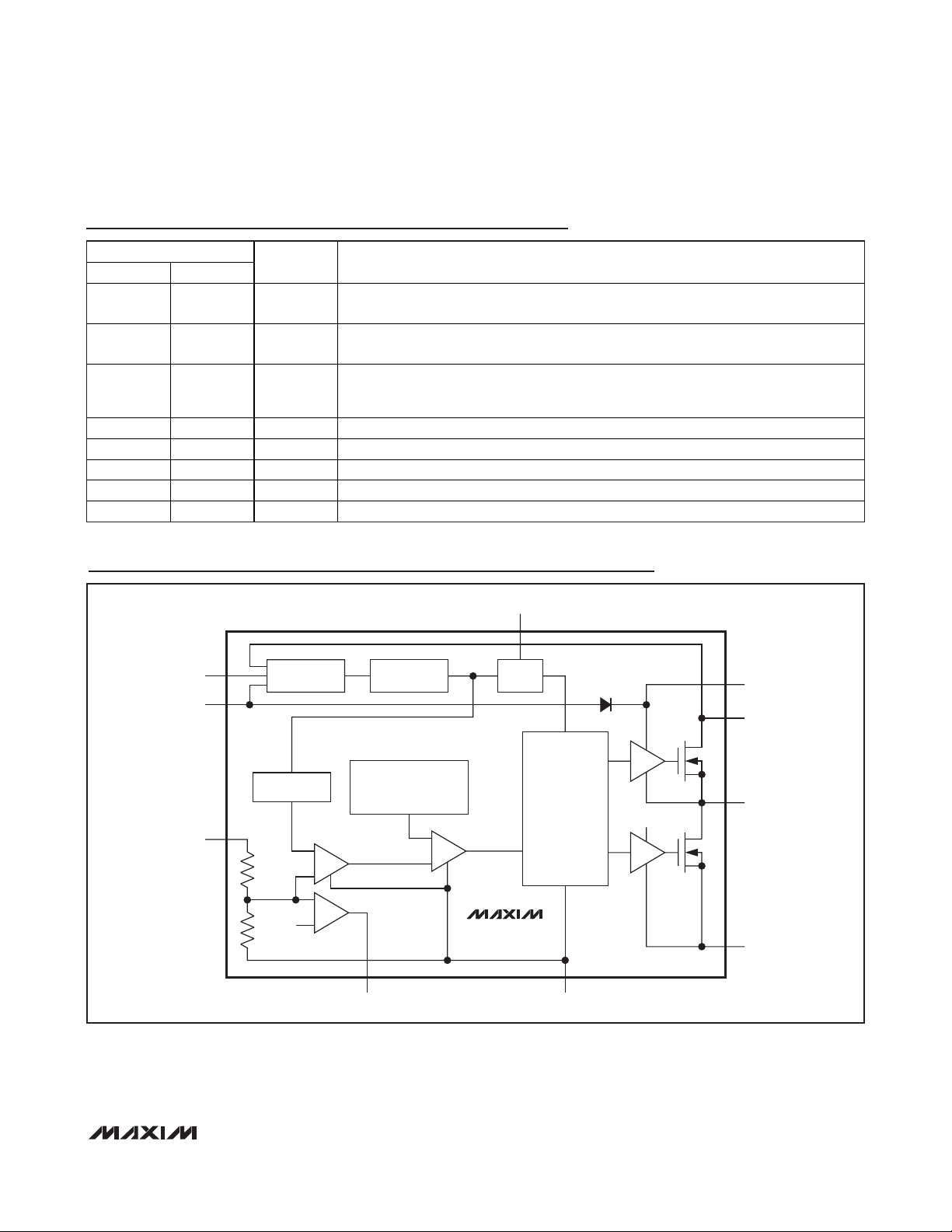
Functional Diagram
PIN
TDFN-EP TSSOP-EP
5 8 OUTS
6 11 PGOOD
7 12 SYNC
8 13 BIAS +5V Internal Logic Supply. Connect a 2.2μF ceramic capacitor from BIAS to GND.
9 14 GND Analog Ground
10 15 EN Enable Input. EN is high-voltage compatible. Drive EN HIGH for normal operation.
9, 10, 16 N.C. No Connection. Not internally connected.
EP Exposed Pad. Connect EP to PGND. Do not use EP as the only ground connection.
NAME FUNCTION
Buc k Regulator Voltage-Sense Input. Bypass OUTS to PGND with a 10μF or larger X7R
ceramic capacitor.
Open-Drain Power-Good Output. External pullup resistor required for automat ic SKIP
mode operation.
Sync Input. SYNC allows the device to synchronize to other supplies. When
connected to GND or unconnected, SKIP mode is enabled under light loads. When
connected to a clock source or BIAS, forced PWM mode is enabled.
SYNC
REF
OSCBANDGAP
CLK
BST
SUP
BIAS
EN
HVLDO
CURRENT-SENSE
SOFT-START
OUTS
EAMP
V
COMP
GOOD
PGOOD
AND
SLOPE COMPENSATION
PWM
LOGIC
CONTROL
MAX16904
GND
HSD
LX
BIAS
LSD
PGND
Page 8

MAX16904
Detailed Description
The MAX16904 is a small, current-mode buck converter
that features synchronous rectification and requires no
external compensation network. The device is designed
for 600mA output current, and can stay in dropout by
running at 97% duty cycle. It provides an accurate output voltage within the +6.5V to +18V input range.
Voltage quality can be monitored by observing the
PGOOD signal. The device operates at 2.1MHz (typ)
frequency, which allows for small external components,
reduced output ripple, and guarantees no AM band
interference.
The device features an ultra-low 25μA (typ) quiescent
supply current in standby mode. Standby mode is
entered when load currents are below 5mA and when
SYNC is low. The device operates from a +3.5V to
+28V supply voltage and tolerates transients up to
+42V, making it ideal for automotive applications. The
device is available in factory-trimmed output voltages
from 1.8V to 10.7V in 100mV steps. Contact the factory
for availability of voltage options.
Enable (EN)
The device is activated by driving EN high. EN is compatible from a +3.3V logic level to automotive battery
levels. EN can be controlled by microcontrollers and
automotive KEY or CAN inhibit signals. The EN input
has no internal pullup/pulldown current to minimize
overall quiescent supply current. To realize a programmable undervoltage lockout level, use a resistordivider from SUP to EN to GND.
BIAS/UVLO
The device features undervoltage lockout. When the
device is enabled, an internal bias generator turns on.
LX begins switching after V
BIAS
has exceeded the inter-
nal undervoltage lockout level V
UVLO
= 3V (typ).
Soft-Start
The device features an internal soft-start timer. The output voltage soft-start ramp time is 8ms (typ). If a short
circuit or undervoltage is encountered, after the softstart timer has expired, the device is disabled for 30ms
(typ) and it reattempts soft-start again. This pattern
repeats until the short circuit has been removed.
Oscillator/Synchronization and
Efficiency (SYNC)
The device has an on-chip oscillator that provides a
switching frequency of 2.1MHz (typ). Depending on the
condition of SYNC, two operation modes exist. If SYNC
is unconnected or at GND, the device must operate in
highly efficient pulse-skipping mode if the load current
is below the SKIP mode current threshold. If SYNC is at
BIAS or has a frequency applied to it, the device is in
forced PWM mode. The device offers the best of both
worlds. The device can be switched during operation
between forced PWM mode and SKIP mode by switching SYNC.
SKIP Mode Operation
SKIP mode is entered when the SYNC pin is connected
to ground or is unconnected and the peak load current
is < 400mA (typ). In this mode, the high-side FET is
turned on until the current in the inductor is ramped up
to 400mA (typ) peak value and the internal feedback
voltage is above the regulation voltage (1.2V typ). At
this point, both the high-side and low-side FETs are
turned off. Depending on the choice of the output
capacitor and the load current the high-side FET turns
on when OUTS (valley) drops below the 1.2V (typ) feedback voltage.
Achieving High Efficiency at Light Loads
The device operates with very low quiescent current at
light loads to enhance efficiency and conserve battery
life. When the device enters SKIP mode the output current is monitored to adjust the quiescent current.
When the output current is < 5mA, the device operates in
the lowest quiescent current mode also called the standby mode. In this mode, the majority of the internal circuitry (excluding that necessary to maintain regulation) in the
device, including the internal high-voltage LDO, is turned
off to save current. Under no load and with SKIP mode
enabled, the device draws only 25μA (typ) current. For
load currents > 5mA, the device enters normal SKIP
mode while still maintaining very high efficiency.
Controlled EMI with Forced-Fixed Frequency
In forced PWM mode, the device attempts to operate at
a constant switching frequency for all load currents. For
tightest frequency control, apply the operating frequency to SYNC. The advantage of this mode is a constant
switching frequency, which improves EMI performance;
the disadvantage is that considerable current can be
thrown away. If the load current during a switching
cycle is less than the current flowing through the inductor, the excess current is diverted to GND. With no
external load present, the operating current is in the
10mA range.
Extended Input Voltage Range
In some cases, the device is forced to deviate from its
operating frequency independent of the state of SYNC.
For input voltages above 18V, the required duty cycle
to regulate its output may be smaller than the minimum
on-time (80ns, typ). In this event, the device is forced to
lower its switching frequency by skipping pulses.
2.1MHz, High-Voltage,
600mA Mini-Buck Converter
8 _______________________________________________________________________________________
Page 9

If the input voltage is reduced and the device
approaches dropout, it tries to turn on the high-side
FET continuously. To maintain gate charge on the highside FET, the BST capacitor must be periodically
recharged. To ensure proper charge on the BST
capacitor when in dropout, the high-side FET is turned
off every 6.5μs and the low-side FET is turned on for
about 150ns. This gives an effective duty cycle
of > 97% and a switching frequency of 150kHz when in
dropout.
Spread-Spectrum Option
The device has an optional spread-spectrum version. If
this option is selected, then the internal operating frequency varies by +6% relative to the internally generated operating frequency of 2.1MHz (typ). Spread
spectrum is offered to improve EMI performance of the
device. By varying the frequency 6% only in the positive direction, the device still guarantees that the
2.1MHz frequency does not drop into the AM band limit
of 1.8MHz. Additionally, with the low minimum on-time
of 80ns (typ) no pulse skipping is observed for a 5V
output with 18V input maximum battery voltage in
steady state.
The internal spread spectrum does not interfere with
the external clock applied on the SYNC pin. It is active
only when the device is running with internally generated switching frequency.
Power-Good (PGOOD)
The device features an open-drain power-good output.
PGOOD is an active-high output that pulls low when the
output voltage is below 91% of its nominal value. The
device is high impedance when the output voltage is
above 93% of its nominal value. Connect a 20kΩ (typ)
pullup resistor to an external supply or the on-chip BIAS
output.
Overcurrent Protection
The device limits the peak output current to 1.5A (typ).
The accuracy of the current limit is ±15%, which makes
selection of external components very easy. To protect
against short-circuit events, the device shuts off when
OUTS is below 1.5V (typ) and one overcurrent event is
detected. The device attempts a soft-start restart every
30ms and stays off if the short circuit has not been
removed. When the current limit is no longer present, it
reaches the output voltage by following the normal softstart sequence. If the device die reaches the thermal
limit of +175°C (typ) during the current-limit event, it
immediately shuts off.
Thermal-Overload Protection
The device features thermal-overload protection. The
device turns off when the junction temperature exceeds
+175°C (typ). Once the device cools by 15°C (typ), it
turns back on with a soft-start sequence.
Applications Information
Inductor Selection
Three key inductor parameters must be specified for
operation with the device: inductance value (L), peak
inductor current (I
PEAK
), and inductor saturation current
(I
SAT
). The minimum required inductance is a function
of operating frequency, input-to-output voltage differential, and the peak-to-peak inductor current
(ΔI
P-P
). Higher ΔI
P-P
allows for a lower inductor value,
while a lower ΔI
P-P
requires a higher inductor value. A
lower inductor value minimizes size and cost, improves
large-signal and transient response, but reduces efficiency due to higher peak currents and higher peak-topeak output-voltage ripple for the same output
capacitor. On the other hand, higher inductance
increases efficiency by reducing the ripple current.
Resistive losses due to extra wire turns can exceed the
benefit gained from lower ripple current levels especially when the inductance is increased without also allowing for larger inductor dimensions. A good compromise
is to choose ΔI
P-P
equal to 30% of the full load current.
Use the following equation to calculate the inductance:
VINand V
OUT
are typical values so that efficiency is
optimum for typical conditions. The switching frequency
is ~2.1MHz. The peak-to-peak inductor current, which
reflects the peak-to-peak output ripple, is worse at the
maximum input voltage. See the
Output Capacitor
section to verify that the worst-case output ripple is acceptable. The inductor saturation current is also important to
avoid runaway current during continuous output short
circuit. The output current may reach 1.725A since this
is the maximum current limit. Choose an inductor with a
saturation current of greater than 1.725A to ensure
proper operation and avoid runaway.
Input Capacitor
The discontinuous input current of the buck converter
causes large input ripple current. The switching frequency, peak inductor current, and the allowable peak-topeak input-voltage ripple dictate the input capacitance
requirement. Increasing the switching frequency or the
MAX16904
2.1MHz, High-Voltage,
600mA Mini-Buck Converter
_______________________________________________________________________________________ 9
()
VVV
OUT IN OUT
L
=
Vf I
IN SW P P
−
××
Δ
−
Page 10

MAX16904
inductor value lowers the peak-to-average current ratio
yielding a lower input capacitance requirement.
The input ripple comprises mainly of ΔVQ(caused by
the capacitor discharge) and ΔV
ESR
(caused by the
ESR of the input capacitor). The total voltage ripple is
the sum of ΔV
Q
and ΔV
ESR
. Assume the input-voltage
ripple from the ESR and the capacitor discharge is
equal to 50% each. The following equations show the
ESR and capacitor requirement for a target voltage ripple at the input:
where:
and:
where I
OUT
is the output current, D is the duty cycle,
and fSWis the switching frequency. Use additional
input capacitance at lower input voltages to avoid possible undershoot below the UVLO threshold during transient loading.
Output Capacitor
The allowable output-voltage ripple and the maximum
deviation of the output voltage during step load currents determine the output capacitance and its ESR.
The output ripple comprises of ΔVQ(caused by the
capacitor discharge) and ΔV
ESR
(caused by the ESR of
the output capacitor). Use low-ESR ceramic or aluminum electrolytic capacitors at the output. For aluminum electrolytic capacitors, the entire output ripple is
contributed by ΔV
ESR
. Use the ESR
OUT
equation to calculate the ESR requirement and choose the capacitor
accordingly. If using ceramic capacitors, assume the
contribution to the output ripple voltage from the ESR
and the capacitor discharge to be equal. The following
equations show the output capacitance and ESR
requirement for a specified output-voltage ripple.
where:
ΔI
P-P
is the peak-to-peak inductor current as calculated
above and f
SW
is the converter’s switching frequency.
The allowable deviation of the output voltage during
fast transient loads also determines the output capacitance and its ESR. The output capacitor supplies the
step load current until the converter responds with a
greater duty cycle. The response time (t
RESPONSE
)
depends on the closed-loop bandwidth of the converter. The device’s high switching frequency allows for a
higher closed-loop bandwidth, thus reducing
t
RESPONSE
and the output capacitance requirement.
The resistive drop across the output capacitor’s ESR
and the capacitor discharge causes a voltage droop
during a step load. Use a combination of low-ESR tantalum and ceramic capacitors for better transient load
and ripple/noise performance. Keep the maximum output-voltage deviations below the tolerable limits of the
electronics being powered. When using a ceramic
capacitor, assume an 80% and 20% contribution from
the output capacitance discharge and the ESR drop,
respectively. Use the following equations to calculate
the required ESR and capacitance value:
where I
STEP
is the load step and t
RESPONSE
is the
response time of the converter. The converter response
time depends on the control-loop bandwidth.
PCB Layout Guidelines
Careful PCB layout is critical to achieve low switching
power losses and clean stable operation. Use a multilayer
board wherever possible for better noise immunity. Refer
to the MAX16904 Evaluation Kit for recommended PCB
layout. Follow these guidelines for a good PCB layout:
1) The input capacitor (4.7μF, see the applications
schematic in the
Typical Operating Circuits
) should be
placed right next to the SUP pins (pins 2 and 3 on the
TSSOP-EP package). Because the device operates at
2.1MHz switching frequency, this placement is critical
for effective decoupling of high-frequency noise from
the SUP pins.
2.1MHz, High-Voltage,
600mA Mini-Buck Converter
10 ______________________________________________________________________________________
ΔI
ESR
C
PP
−
IN
=
Δ
V
=
IDD
=
VV V
()
D
ESR
Δ
⎛
I
⎜
OUT
⎝
OUT
ΔVf
IN OUT OUT
Vf L
=
I
⎞
−
PP
+
×−
×
QSW
⎟
⎠
2
1(
))
−×
××
IN SW
V
OUT
V
IN
ESR
C
=
OUT
Δ
V
ESR
=
Δ
I
PP
−
I
Δ
PP
−
Vf
Δ8
××
QSW
ΔI
PP
V
OUT RIPPLE
VV V
−×
()
IN OUT OUT
=
−
Vf L
IN SW
_
≅≅+ΔΔVV
××
ESR Q
V
Δ
ESR
=
I
STEP
×
V
Δ
Q
ESR
OUT
It
C
OUT
STEP RESPONSE
=
Page 11

2) Solder the exposed pad to a large copper plane
area under the device. To effectively use this copper
area as heat exchanger between the PCB and ambient, expose the copper area on the top and bottom
side. Add a few small vias or one large via on the
copper pad for efficient heat transfer. Connect the
exposed pad to PGND ideally at the return terminal
of the output capacitor.
3) Isolate the power components and high current
paths from sensitive analog circuitry.
4) Keep the high current paths short, especially at the
ground terminals. The practice is essential for stable
jitter-free operation.
5) Connect the PGND and GND together preferably at
the return terminal of the output capacitor. Do not
connect them anywhere else.
6) Keep the power traces and load connections short.
This practice is essential for high efficiency. Use
thick copper PCB to enhance full load efficiency and
power dissipation capability.
7) Route high-speed switching nodes away from sensitive analog areas. Use internal PCB layers as PGND
to act as EMI shields to keep radiated noise away
from the device and analog bypass capacitor.
ESD Protection
The device’s ESD tolerance is rated for Human Body
Model and Machine Model. The Human Body Model
discharge components are CS= 100pF and RD= 1.5kΩ
(Figure 1). The Machine Model discharge components
are CS= 200pF and RD= 0Ω (Figure 2).
MAX16904
2.1MHz, High-Voltage,
600mA Mini-Buck Converter
______________________________________________________________________________________ 11
Figure 1. Human Body ESD Test Circuit
Figure 2. Machine Model ESD Test Circuit
R
D
HIGH-
VOLTAGE
DC
SOURCE
1MΩ
CHARGE-CURRENT-
LIMIT RESISTOR
C
100pF
S
1.5kΩ
DISCHARGE
RESISTANCE
STORAGE
CAPACITOR
DEVICE
UNDER
TEST
R
D
0Ω
HIGH-
VOLTAGE
DC
SOURCE
CHARGE-CURRENT-
LIMIT RESISTOR
200pF
C
S
DISCHARGE
RESISTANCE
STORAGE
CAPACITOR
DEVICE
UNDER
TEST
Page 12

MAX16904
2.1MHz, High-Voltage,
600mA Mini-Buck Converter
12 ______________________________________________________________________________________
Chip Information
PROCESS: BiCMOS
Selector Guide
PART
OUTPUT VOLTAGE
(V)
PIN-PACKAGE
SPREAD-SPECTRUM
SWITCHING FREQUENCY
TOP
MAX16904RATB50/V+ 5
10 TDFN-EP*
⎯ AVY
MAX16904RAUE50/V+ 5
16 TSSOP-EP*
(5mm x 4.4mm)
⎯⎯
MAX16904SATB50/V+ 5
10 TDFN-EP*
Yes AWA
MAX16904SAUE50/V+ 5
16 TSSOP-EP*
(5mm x 4.4mm)
Yes ⎯
MAX16904RATB33/V+ 3.3
10 TDFN-EP*
⎯ AVX
MAX16904RAUE33/V+ 3.3
16 TSSOP-EP*
(5mm x 4.4mm)
⎯⎯
MAX16904SATB33/V+ 3.3
10 TDFN-EP*
Yes AVZ
MAX16904SAUE33/V+ 3.3
16 TSSOP-EP*
(5mm x 4.4mm)
Yes ⎯
MAX16904RAUE18/V+ 1.8
16 TSSOP-EP*
(5mm x 4.4mm)
⎯⎯
Note: All devices operate over the -40°C to +125°C automotive temperature range.
+
Denotes a lead(Pb)-free/RoHS-compliant package.
/V denotes an automotive qualified part.
*
EP = Exposed pad.
Package Information
For the latest package outline information and land patterns,
go to www.maxim-ic.com/packages
. Note that a “+”, “#”, or
“-” in the package code indicates RoHS status only. Package
drawings may show a different suffix character, but the drawing
pertains to the package regardless of RoHS status.
PACKAGE
TYPE
PACKAGE
CODE
OUTLINE
NO.
LAND
PATTERN NO.
10 TDFN-EP T1033+1
21-0137 90-0003
16 TSSOP-EP U16E+3
21-0108 90-0120
(3mm x 3mm x 0.75mm)
MARK
(3mm x 3mm x 0.75mm)
(3mm x 3mm x 0.75mm)
(3mm x 3mm x 0.75mm)
Page 13
MAX16904
2.1MHz, High-Voltage,
600mA Mini-Buck Converter
Maxim cannot assume responsibility for use of any circuitry other than circuitry entirely embodied in a Maxim product. No circuit patent licenses are
implied. Maxim reserves the right to change the circuitry and specifications without notice at any time.
Maxim Integrated Products, 120 San Gabriel Drive, Sunnyvale, CA 94086 408-737-7600 ____________________
13
© 2010 Maxim Integrated Products Maxim is a registered trademark of Maxim Integrated Products, Inc.
Revision History
REVISION
NUMBER
0 9/10 Initial release —
1 11/10 Added new output voltage trim to Selector Guide 12
REVISION
DATE
DESCRIPTION
PAGES
CHANGED
 Loading...