

Page 1
General Description
The MAX16834 is a current-mode high-brightness LED
(HB LED) driver for boost, buck-boost, SEPIC, and highside buck topologies. In addition to driving an n-channel
power MOSFET switch controlled by the switching controller, it also drives an n-channel PWM dimming switch to
achieve LED PWM dimming. The MAX16834 integrates
all the building blocks necessary to implement a fixed-frequency HB LED driver with wide-range dimming control.
The MAX16834 features constant-frequency peak current-mode control with programmable slope compensation to control the duty cycle of the PWM controller.
A dimming driver designed to drive an external n-channel MOSFET in series with the LED string provides
wide-range dimming control up to 20kHz. In addition to
PWM dimming, the MAX16834 provides analog dimming using a DC input at REFI. The programmable
switching frequency (100kHz to 1MHz) allows design
optimization for efficiency and board space reduction.
A single resistor from RT/SYNC to ground sets the
switching frequency from 100kHz to 1MHz while an
external clock signal at RT/SYNC disables the internal
oscillator and allows the MAX16834 to synchronize to
an external clock. The MAX16834’s integrated highside current-sense amplifier eliminates the need for a
separate high-side LED current-sense amplifier in
buck-boost applications.
The MAX16834 operates over a wide supply range of
4.75V to 28V and includes a 3A sink/source gate driver
for driving a power MOSFET in high-power LED driver
applications. The MAX16834 is also suitable for DC-DC
converter applications such as boost or buck-boost.
Additional features include external enable/disable
input, an on-chip oscillator, fault indicator output (FLT)
for LED open/short or overtemperature conditions, and
an overvoltage protection sense input (OVP+) for true
overvoltage protection.
The MAX16834 is available in a thermally enhanced
4mm x 4mm, 20-pin TQFN-EP package and is specified
over the automotive -40°C to +125°C temperature range.
Applications
Single-String LED LCD Backlighting
Automotive Rear and Front Lighting
Projection System RGB LED Light Sources
Architectural and Decorative Lighting (MR16, M111)
Spot and Ambient Lights
DC-DC Boost/Buck-Boost Converters
Features
o Wide Input Operating Voltage Range (4.75V to
28V)
o 3000:1 PWM Dimming
o Analog Dimming
o Integrated PWM Dimming MOSFET Driver
o Integrated High-Side Current-Sense Amplifier for
LED Current Sense in Buck-Boost Converter
o 100kHz to 1MHz Programmable High-Frequency
Operation
o External Clock Synchronization Input
o Programmable UVLO
o Internal 7V Low-Dropout Regulator
o Fault Output (FLT) for Overvoltage, Overcurrent,
and Thermal Warning Faults
o Programmable True Differential Overvoltage
Protection
o 20-Pin TQFN-EP Package
MAX16834
High-Power LED Driver with Integrated High-Side LED
Current Sense and PWM Dimming MOSFET Driver
________________________________________________________________
Maxim Integrated Products
1
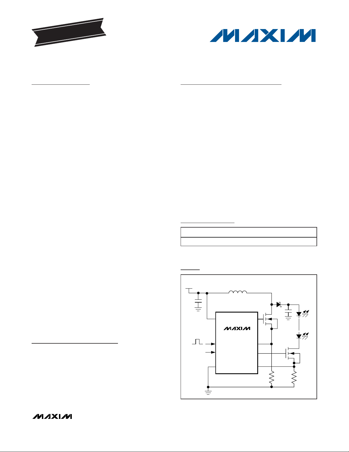
Simplified Application Circuit
Ordering Information
19-4235; Rev 0; 8/08
For pricing, delivery, and ordering information, please contact Maxim Direct at 1-888-629-4642,
or visit Maxim’s website at www.maxim-ic.com.
EVALUATION KIT
AVAILABLE
+
Denotes a lead-free/RoHS-compliant package.
*
EP = Exposed pad.
PART TEMP RANGE
PIN-PACKAGE
MAX16834ATP+
-40°C to +125°C 20 TQFN-EP*
Pin Configuration appears at end of data sheet.
IN
MAX16834
PWMDIM
REFI
PGND
BOOST LED DRIVER
NDRV
CS
DIMOUT
SENSE+
LED+
LEDs
LED-
V
OFF
IN
ANALOG
ON
DIM
Page 2
MAX16834
High-Power LED Driver with Integrated High-Side LED
Current Sense and PWM Dimming MOSFET Driver
2 _______________________________________________________________________________________
ABSOLUTE MAXIMUM RATINGS
ELECTRICAL CHARACTERISTICS
(VIN= VHV= 12V, V
UVEN
= 5V, VLV= V
PWMDIM
= SGND, C
VCC
= 4.7µF, C
LCV
= 100nF, C
REF
= 100nF, R
SENSE+
= 0.1Ω,
R
RT
= 10kΩ, TA= TJ= -40°C to +125°C, unless otherwise noted. Typical values are at TA= +25°C.)
Stresses beyond those listed under “Absolute Maximum Ratings” may cause permanent damage to the device. These are stress ratings only, and functional
operation of the device at these or any other conditions beyond those indicated in the operational sections of the specifications is not implied. Exposure to
absolute maximum rating conditions for extended periods may affect device reliability.
Note 1: Package thermal resistances were obtained using the method described in JEDEC specification JESD51-7, using a four-
layer board. For detailed information on package thermal considerations, refer to www.maxim-ic.com/thermal-tutorial
.
IN, HV, LV to SGND................................................-0.3V to +30V
OVP+, SENSE+, DIMOUT, CLV to SGND ..............-0.3V to +30V
SENSE+ to LV........................................................-0.3V to +0.3V
HV, IN to LV ............................................................-0.3V to +30V
OVP+, CLV, DIMOUT to LV ......................................-0.3V to +6V
PGND to SGND .....................................................-0.3V to +0.3V
V
CC
to SGND..........................................................-0.3V to +12V
NDRV to PGND...........................................-0.3V to (V
CC
+ 0.3V)
All Other Pins to SGND.............................................-0.3V to +6V
NDRV Continuous Current................................................±50mA
DIMOUT Continuous Current..............................................±2mA
V
CC
Short-Circuit Current to SGND Duration ...........................1s
Continuous Power Dissipation (T
A
= +70°C)
20-Pin TQFN 4mm x 4mm
(derate 25.6mW/°C* above +70°C) ............................2051mW
Junction-to-Ambient Thermal Resistance (
θ
JA
) (Note 1).....39°C/W
Junction-to-Case Thermal Resistance (
θ
JC
) (Note 1) ........6°C/W
Operating Temperature Range .........................-40°C to +125°C
Junction Temperature......................................................+150°C
Storage Temperature Range .............................-65°C to +150°C
Lead Temperature (soldering, 10s) .................................+300°C
*
As per JEDEC51 standard (multilayer board).
Input Voltage Range V
Quiescent Supply Current I
Shutdown Supply Current I
INTERNAL LINEAR REGULATOR (VCC)
Output Voltage V
Dropout Voltage V
Short-Circuit Current VCC = 0V, VIN = 12V 80 300 mA
LINEAR REGULATOR (CLV)
Output Voltage (V
Dropout Voltage V
Short-Circuit Current V
REFERENCE VOLTAGE (REF)
Output Voltage V
REF Short-Circuit Current V
UNDERVOLTAGE LOCKOUT/ENABLE INPUT (UVEN)
UVEN On Threshold Voltage V
UVEN Threshold Voltage
Hysteresis
Input Leakage Current I
PWMDIM
PWMDIM On Threshold Voltage V
PWMDIM Threshold Voltage
Hysteresis
Input Leakage Current V
PARAMETER SYMBOL CONDITIONS MIN TYP MAX UNITS
IN
Q
SHDN
CC
OD
CLV - VLV
DO
REF
UVEN_THUP
LEAK
PWMDIM
Excluding I
V
UVEN
0 ≤ ICC ≤ 50mA, 9.5V ≤ VIN ≤ 28V 6.3 7 7.7 V
ICC = 35mA (Note 2) 0.65 1.8 V
0 ≤ I
CLV
)
6V ≤ V
I
= 2mA, 0 ≤ VLV ≤ 23.3V (Note 3) 0.5 V
CLV
= 12V, VIN = 12V, VHV = 24V 2.2 10 mA
CLV
0 ≤ I
REF
= 0 30 mA
REF
V
UVEN
PWMDIM
LED
= 0 30 60 µA
≤ 2mA, 6V ≤ VHV ≤ 28V,
≤ 22V
(HV-LV)
≤ 1mA, 4.75V ≤ VIN ≤ 28V 3.625 3.70 3.775 V
= 0 I1I µA
= 0 I1I µA
4.75 28 V
4.7 5 5.3 V
1.395 1.435 1.475 V
200 mV
1.395 1.435 1.475 V
200 mV
610mA
Page 3
MAX16834
High-Power LED Driver with Integrated High-Side LED
Current Sense and PWM Dimming MOSFET Driver
_______________________________________________________________________________________ 3
ELECTRICAL CHARACTERISTICS (continued)
(VIN= VHV= 12V, V
UVEN
= 5V, VLV= V
PWMDIM
= SGND, C
VCC
= 4.7µF, C
LCV
= 100nF, C
REF
= 100nF, R
SENSE+
= 0.1Ω,
R
RT
= 10kΩ, TA= TJ= -40°C to +125°C, unless otherwise noted. Typical values are at TA= +25°C.)
OSCILLATOR
Oscillator Frequency f
Oscillator Frequency Range (Note 4) 100 1000 kHz
External Sync Input Clock High
Threshold
External Sync Input Clock Low
Threshold
External Sync Input High Pulse
Width
Maximum External Sync Period 50 µs
SLOPE COMPENSATION (SC)
SC Pullup Current I
SC Discharge Resistance R
REFI
REFI Input Bias Current V
REFI Input Common-Mode Range (Note 4) 0 2 V
SENSE+
SENSE+ Input Bias Current (V
HIGH-SIDE LED CURRENT-SENSE AMPLIFIER (V
Input Offset Voltage VLV > 5V, (V
Voltage Gain A
3dB Bandwidth
LOW-SIDE LED CURRENT-SENSE AMPLIFIER
Input Offset Voltage VLV < 1V, (V
Voltage Gain A
3dB Bandwidth 600 kHz
CURRENT ERROR AMPLIFIER (TRANSCONDUCTANCE AMPLIFIER)
Transconductance g
Open-Loop DC Gain A
Input Offset Voltage -10 0 +10 mV
COMP Voltage Range V
PWM COMPARATOR
Input Offset Voltage 0.6 0.65 0.70 V
Propagation Delay t
Minimum On-Time t
Duty Cycle (Note 4) 90 99.5 %
PARAMETER SYMBOL CONDITIONS MIN TYP MAX UNITS
OSC
SCPU
SCD
V
V
m
V
COMP
PD
ON(MIN)
R
RT/SYNC
R
RT/SYNC
(Note 4) 2 V
(Note 4) 0.4 V
(Note 4) 200 ns
VSC = 100mV 80 100 120 µA
VSC = 100mV 8 Ω
REFI
VLV > 5V, (V
(V
(V
VLV < 1V, (V
V
COMP
(Note 4) 0.4 2.5 V
50mV overdrive 40 ns
On-time includes blanking time 100 ns
= 5kΩ 0.9 1 1.1 MHz
= 25kΩ 180 200 220 kHz
= 1V I1I µA
- VLV) = 100mV 250 µA
SENSE+
- VLV)
SENSE+
- VLV) = 0.1V, no load 1.8 MHz
SENSE+
- VLV) = 0.02V, no load 600 kHz
SENSE+
= 2V, V
- VLV) = 5mV -2.4 0 +2.4 mV
SENSE+
- VLV) = 0.2V 9.7 9.9 10.1 V/V
SENSE+
- VLV) = 0V -2 0 +2 mV
SENSE+
- VLV) = 0.2V 9.7 9.9 10.1 V/V
SENSE+
= 5V 400 500 600 µS
PWMDIM
60 dB
Page 4
MAX16834
High-Power LED Driver with Integrated High-Side LED
Current Sense and PWM Dimming MOSFET Driver
4 _______________________________________________________________________________________
ELECTRICAL CHARACTERISTICS (continued)
(VIN= VHV= 12V, V
UVEN
= 5V, VLV= V
PWMDIM
= SGND, C
VCC
= 4.7µF, C
LCV
= 100nF, C
REF
= 100nF, R
SENSE+
= 0.1Ω,
R
RT
= 10kΩ, TA= TJ= -40°C to +125°C, unless otherwise noted. Typical values are at TA= +25°C.)
Note 2: Dropout voltage is defined as VIN- VCC, when VCCis 100mV below the value of VCCfor VIN= 9.5V.
Note 3: Dropout is defined as V
HV
- V
CLV
, when V
CLV
is 100mV below the value of V
CLV
for VHV= 8V.
Note 4: Not production tested. Guaranteed by design.
CURRENT PEAK LIMIT COMPARATOR
Trip Threshold Voltage 0.25 0.3 0.35 V
Propagation Delay 50mV overdrive with respect to NDRV 40 ns
OVERVOLTAGE PROTECTION INPUT (OVP+)
OVP+ On Threshold Voltage V
OVP+ Hysteresis 200 mV
OVP+ Input Leakage Current (V
HIGH-SIDE LED SHORT COMPARATOR
Off Threshold V
On Threshold V
Error Reject Blankout f
LOW-SIDE LED SHORT COMPARATOR
Off Threshold 0.27 0.30 0.33 V
Error Reject Blankout 5µs
HICCUP TIMER
Hiccup Time f
GATE-DRIVER OUTPUT (NDRV)
NDRV Peak Pullup Current VCC = 7V 3 A
NDRV Peak Pulldown Current VCC = 7V 3 A
p-Channel MOSFET R
n-Channel MOSFET R
DIMOUT
DIMOUT Peak Pullup Current (V
DIMOUT Peak Pulldown Current (V
p-Channel MOSFET R
n-Channel MOSFET R
PWMDIM to DIMOUT
Propagation Delay
FAULT FLAG (FLT)
FLT Pulldown Current V
FLT Leakage Current V
Thermal Warning On Threshold +140 °C
Thermal Warning Threshold
Hysteresis
PARAMETER SYMBOL CONDITIONS MIN TYP MAX UNITS
DSON
DSON
DSON
DSON
OVP_ON
- VLV) = 1.235V -1 +1 µA
OVP
- V
CLV
LV
- V
CLV
LV
= 500kHz 256 µs
OSC
= 500kHz 8.2 ms
OSC
(VCC - V
V
(V
(V
NDRV
= 0.1V 0.9 1.7 Ω
NDRV
- VLV) = 5V 25 50 mA
CLV
- VLV) = 5V 25 50 mA
CLV
- V
CLV
DIMOUT
- VLV) = 0.1V 25 Ω
DIMOUT
= 0.2V 2 5 10 mA
FLT
= 1.0V I1I µA
FLT
) = 0.1V 1.2 1.9 Ω
) = 0.1V 31 Ω
1.375 1.435 1.495 V
4.0 4.3 4.6 V
4.1 4.4 4.7 V
200 ns
20 °C
Page 5
MAX16834
High-Power LED Driver with Integrated High-Side LED
Current Sense and PWM Dimming MOSFET Driver
_______________________________________________________________________________________ 5
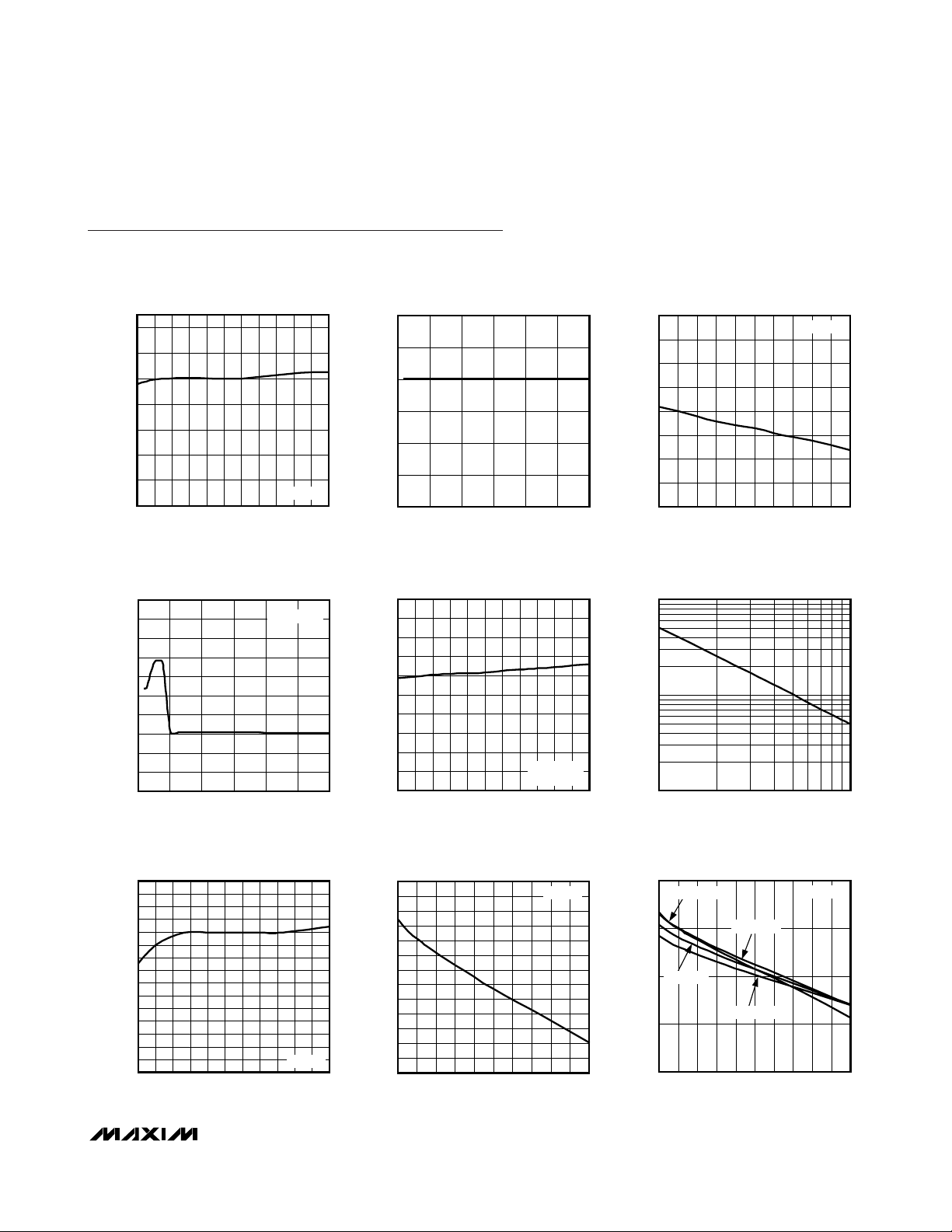
V
(V)
Typical Operating Characteristics
(VIN= VHV= 12V, V
UVEN
= 5V, VLV= V
PWMDIM
= SGND, C
VCC
= 4.7µF, C
LCV
= 100nF, C
REF
= 100nF, R
SENSE+
= 0.1Ω,
R
RT
= 10kΩ, TA= +25°C, unless otherwise noted.)
V
vs. TEMPERATURE
REF
3.74
3.72
3.70
(V)
3.68
REF
V
3.66
3.64
3.62
3.60
-40 125
TEMPERATURE (°C)
VIN = 12V
11095-25 -10 5 35 50 6520 80
SUPPLY CURRENT
vs. SUPPLY VOLTAGE
20
18
16
14
12
10
8
6
SUPPLY CURRENT (mA)
4
2
0
428
SUPPLY VOLTAGE (V)
PWMDIM = 0
242016128
3.80
3.75
MAX16834 toc01
3.70
(V)
3.65
REF
V
3.60
3.55
3.50
10
9
MAX16834 toc04
8
7
6
5
4
3
SUPPLY CURRENT (mA)
2
1
0
V
REF
428
vs. TEMPERATURE
-40 125
vs. SUPPLY VOLTAGE
SUPPLY VOLTAGE (V)
SUPPLY CURRENT
VIN = 12V
PWMDIM = 0
TEMPERATURE (°C)
242016128
1109565 80-10 5 20 35 50-25
3.7020
3.7015
MAX16834 toc02
3.7010
3.7005
3.7000
REF
3.6995
3.6990
3.6985
3.6980
100
MAX16834 toc05
10
RT (kΩ)
1
V
vs. I
REF
010
I
(mA)
REF
RT vs. SWITCHING FREQUENCY
VIN = 12V
SWITCHING FREQUENCY (kHz)
REF
VIN = 12V
MAX16834 toc03
981 2 3 5 64 7
MAX16834 toc06
1000100
SWITCHING FREQUENCY
605
604
603
602
601
600
599
598
597
596
595
594
SWITCHING FREQUENCY (kHz)
593
592
591
590
-40 125
TEMPERATURE (°C)
VIN = 12V
1109565 80-10 5 20 35 50-25
MAX16834 toc07
7.16
7.14
7.12
7.10
7.08
7.06
(V)
7.04
CC
7.02
V
7.00
6.98
6.96
6.94
6.92
6.90
0100
vs. TEMPERATURE
VCC vs. I
ICC (mA)
CC
VIN = 12V
908060 7020 30 40 5010
MAX16834 toc08
7.2
TA = +125°C
7.1
(V)
7.0
TA = +25°C
CC
V
6.9
6.8
0100
VCC vs. I
TA = +100°C
TA = -40°C
ICC (mA)
CC
VIN = 12V
MAX16834 toc09
908070605040302010
Page 6
Pin Description
MAX16834
High-Power LED Driver with Integrated High-Side LED
Current Sense and PWM Dimming MOSFET Driver
6 _______________________________________________________________________________________
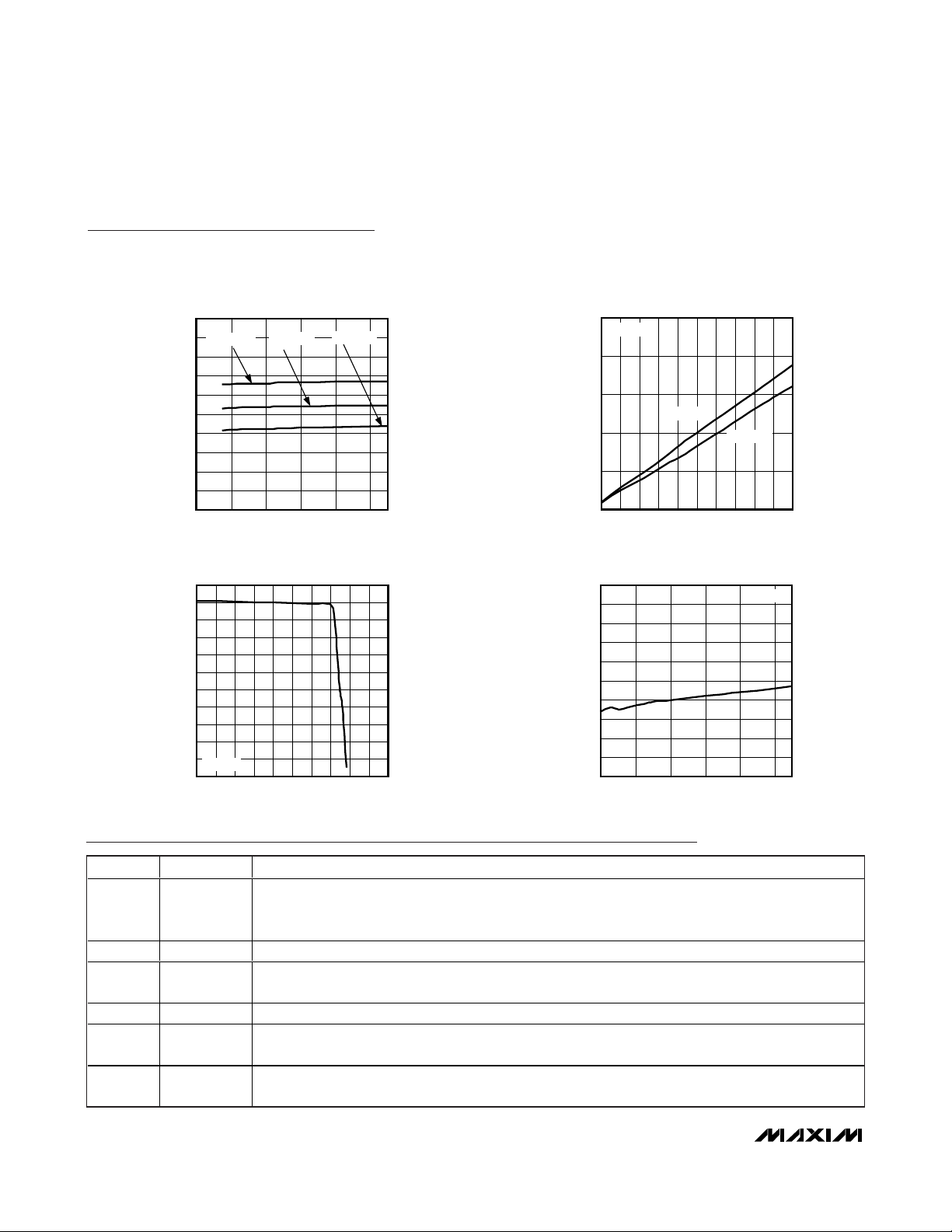
Typical Operating Characteristics (continued)
(VIN= VHV= 12V, V
UVEN
= 5V, VLV= V
PWMDIM
= SGND, C
VCC
= 4.7µF, C
LCV
= 100nF, C
REF
= 100nF, R
SENSE+
= 0.1Ω,
R
RT
= 10kΩ, TA= +25°C, unless otherwise noted.)
VCC vs. V
IN
MAX16834 toc10
VIN (V)
V
CC
(V)
26
22
1814
10
7.02
7.04
7.06
7.08
7.10
7.12
7.14
7.16
7.18
7.20
7.00
6
TA = +125°C
TA = +25°C
TA = -40°C
NDRV RISE/FALL TIME
vs. CAPACITANCE
MAX16834 toc11
CAPACITANCE (nF)
NDRV RISE TIME (ns)
987654321
10
20
30
40
50
0
010
VIN = 12V
RISE TIME
FALL TIME
V
CLV
vs. V
HV
MAX16834 toc13
VHV (V)
V
CLV
(V)
26
22
18
14
10
5.01
5.02
5.03
5.04
5.05
5.06
5.07
5.08
5.09
5.10
5.00
6
VIN = 12V
V
CLV
vs. I
CLV
MAX16834 toc12
I
CLV
(mA)
V
CLV
(V)
4.54.03.0 3.51.0 1.5 2.0 2.50.5
0.50
1.00
1.50
2.00
2.50
3.00
3.50
4.00
4.50
5.00
5.50
0
05.0
VIN = 12V
PIN NAME FUNCTION
LED-String Overvoltage Protection Input. Connect a resistive voltage-divider between the positive
1 OVP+
2 SGND Signal Ground
3 COMP
4 REF 3.7V Reference Output Voltage. Bypass REF to SGND with a 0.1µF to 0.22µF ceramic capacitor.
5 REFI
6SC
output, OVP+, and LV to set the overvoltage threshold. OVP+ has a 1.435V threshold voltage with a
200mV hysteresis.
Error-Amplifier Output. Connect an RC network from COMP to SGND for stable operation. See the
Feedback Compensation section.
Current Reference Input. V
provides a reference voltage for the current-sense amplifier to set the
REFI
LED current.
Current-Mode Slope Compensation Setting. Connect to an appropriate external capacitor from SC to
SGND to generate a ramp signal for stable operation.
Page 7
MAX16834
High-Power LED Driver with Integrated High-Side LED
Current Sense and PWM Dimming MOSFET Driver
_______________________________________________________________________________________ 7
Pin Description (continued)
Detailed Description
The MAX16834 is a current-mode, high-brightness LED
(HB LED) driver designed to control a single-string LED
current regulator with two external n-channel MOSFETs.
The MAX16834 integrates all the building blocks necessary to implement a fixed-frequency HB LED driver
with wide-range dimming control. The MAX16834
allows implementation of different converter topologies
such as SEPIC, boost, buck-boost, or high-side buck
current regulator.
The MAX16834 features a constant-frequency, peak-current-mode control with programmable slope compensation to control the duty cycle of the PWM controller. A
dimming driver offers a wide-range dimming control for
the external n-channel MOSFET in series with the LED
string. In addition to PWM dimming, the MAX16834
allows for analog dimming of LED current.
The MAX16834 switching frequency (100kHz to 1MHz)
is adjustable using a single resistor from RT/SYNC. The
MAX16834 disables the internal oscillator and synchronizes if an external clock is applied to RT/SYNC. The
switching MOSFET driver sinks and sources up to 3A,
making it suitable for high-power MOSFETs driving in
HB LED applications, and the dimming control allows
for wide PWM dimming at frequencies up to 20kHz.
The MAX16834 is suitable for boost and buck-boost
LED drivers (Figures 2 and 3).
The MAX16834 operates over a wide 4.75V to 28V supply range. Additional features include external
enable/disable input, an on-chip oscillator, fault indicator output (FLT) for LED open/short or overtemperature
conditions, and an overvoltage protection circuit for
true differential overvoltage protection (Figure 1).
The MAX16834 is also suitable for DC-DC converter
applications such as boost or buck-boost (Figures 6
and 7). Other applications include boost LED drivers
with automotive load dump protection (Figure 4) and
high-side buck LED drivers (Figure 5).
PIN NAME FUNCTION
7 FLT Active-Low, Open-Drain Fault Indicator Output. See the Fault Indicator (
Resistor-Programmable Switching Frequency Setting/Sync Control Input. Connect a resistor from
8 RT/SYNC
9 UVEN
10 PWMDIM PWM Dimming Input. Connect to an external PWM signal for dimming operation.
11 CS
12 PGND Power Ground
13 NDRV External n-Channel Gate-Driver Output
14 V
15 IN Positive Power-Supply Input. Bypass to PGND with at least a 0.1µF ceramic capacitor.
16 HV High-Side Positive Supply Input Referred to LV. HV provides power to high-side linear regulator CLV.
17 CLV
18 DIMOUT External Dimming MOSFET Gate Driver. DIMOUT is capable of sinking/sourcing 50mA.
19 LV
20 SENSE+ LED Current-Sense Positive Input
—EP
CC
RT/SYNC to SGND to set the switching frequency. Drive RT/SYNC to synchronize the switching
frequency with an external clock.
Undervoltage-Lockout (UVLO) Threshold/Enable Input. UVEN is a dual-function adjustable UVLO
threshold input with an enable feature. Connect UVEN to VIN through a resistive voltage-divider to
program the UVLO threshold. Observe the absolute maximum value for this pin.
Current-Sense Amplifier Positive Input. Connect a resistor from CS to PGND to set the inductor peak
current limit.
7V Low-Dropout Voltage Regulator. Bypass to PGND with at least a 1µF low-ESR ceramic capacitor.
provides power to the n-channel gate driver (NDRV).
V
CC
5V High-Side Regulator Output. CLV provides power to the dimming MOSFET driver. Connect a 0.1µF
to 1µF ceramic capacitor from CLV to LV for stable operation.
High-Side Reference Voltage Input. Connect to SGND for boost configuration. Connect to IN for buckboost configuration.
Exposed Pad. Connect EP to a large-area contiguous copper ground plane for effective power
dissipation. Do not use as the main IC ground connection. EP must be connected to SGND.
FLT
) section.
Page 8
MAX16834
High-Power LED Driver with Integrated High-Side LED
Current Sense and PWM Dimming MOSFET Driver
8 _______________________________________________________________________________________
Figure 1. Internal Block Diagram
IN
SGND
UVEN
RT/SYNC
SC
CS
REFI
SENSE+
1kΩ
V
LV
COMP
HV
V
LV
PWMDIM
OVP+
BG
V
REFERENCE
V
BG
OSC
5kΩ
BLANK
NDRVB
LPF
V
LV
HIGH-SIDE
REGULATOR
BG
V
AV = 9.9
5V
V
HV
REF
V
FLTA
7V
LDO
UVLO
RAMP
GENERATOR
CURRENT-LIMIT
COMPARATOR
0.3V
LED CURRENTSENSE AMPLIFIERS
LV REFERENCE
SWITCH
BG
FLTB
ERROR
AMPLIFIER
g
REFHI
AND
TO
INTERNAL
CIRCUITRY
m
0.6V
V
LV
TEMPERATURE
PWM
COMP
4.3V
0.3V
SENSE+
SENSE
V
OR
PWMDIM
V
IN
REF
OT
OT
S
Q
R
AND
V
LV
128 TOSC
ERROR
REJECT
DELAY
5µs ERROR
REJECT
DELAY
AND
REFHI
FLTAFLTB
NDRVB
4096 TOSC
HICCUP
TIMER
AND
FLTB
REF
V
CC
NDRV
PGND
FLT
CLV
DIMOUT
V
BG
V
LV
V
LV
MAX16834
Page 9

MAX16834
Undervoltage Lockout/Enable
The MAX16834 features an adjustable UVLO using the
enable input (UVEN). Connect UVEN to VINthrough a
resistive divider to set the UVLO threshold. The
MAX16834 is enabled when the V
UVEN
exceeds the
1.435V (typ) threshold. See the
Setting the UVLO
Threshold
section for more information.
UVEN also functions as an enable/disable input to the
device. Drive UVEN low to disable the output and high
to enable the output.
Reference Voltage (REF)
The MAX16834 features a 3.7V reference output, REF.
REF provides power to most of the internal circuit blocks
except for the output drivers and is capable of sourcing
1mA to external circuits. Connect a 0.1µF to 0.22µF
ceramic capacitor from REF to SGND. Connect REF to
REFI through a resistive divider to set the LED current.
Reference Input (REFI)
The output current is proportional to the voltage at
REFI. Applying an external DC voltage at REFI or using
a potentiometer from REF to SGND allows analog dimming of the output current.
High-Side Reference Voltage Input (LV)
LV is a reference input. Connect LV to SGND for boost
and SEPIC topologies. Connect LV to IN for buck-boost
and high-side buck topologies.
Dimming Driver Regulator
Input Voltage (HV)
The voltage at HV provides the input voltage for the
dimming driver regulator. For boost or SEPIC topology,
connect HV either to IN or to VCC. For buck-boost, connect HV to a voltage higher than IN. The voltage at HV
must not exceed 28V with respect to PGND. For the
high-side buck, connect HV to IN.
Dimming MOSFET Driver (DIMOUT)
The MAX16834 requires an external n-channel MOSFET
for PWM dimming. Connect the gate of the MOSFET to
the output of the dimming driver, DIMOUT, for normal
operation. The dimming driver is capable of sinking or
sourcing up to 50mA of current.
n-Channel MOSFET Switch Driver (NDRV)
The MAX16834 drives an external n-channel switching
MOSFET. NDRV swings between VCCand PGND.
NDRV is capable of sinking/sourcing 3A of peak current,
allowing the MAX16834 to switch MOSFETs in highpower applications. The average current demanded
from the supply to drive the external MOSFET depends
on the total gate charge (QG) and the operating
frequency of the converter, fSW. Use the following equation to calculate the driver supply current I
NDRV
required for the switching MOSFET:
I
NDRV
= QGx f
SW
Pulse Dimming Inputs (PWMDIM)
The MAX16834 offers a dimming input (PWMDIM) for
pulse-width modulating the output current. PWM dimming can be achieved by driving PWMDIM with a pulsating voltage source. When the voltage at PWMDIM is
greater than 1.435V, the PWM dimming MOSFET turns
on and when the voltage on PWMDIM is below 1.235V,
the PWM dimming MOSFET turns off.
High-Side Linear Regulator (V
CLV
)
The MAX16834’s 5V high-side regulator (CLV) powers
up the dimming MOSFET driver. V
CLV
is measured with
respect to LV and sources up to 2mA of current.
Bypass CLV to LV with a 0.1µF to 1µF low-ESR ceramic
capacitor. The maximum voltage on CLV with respect
to PGND must not exceed 28V. This limits the input voltage for buck-boost topology.
Low-Side Linear Regulator (VCC)
The MAX16834’s 7V low-side linear regulator (VCC) powers up the switching MOSFET driver with sourcing capability of up to 50mA. Use at least a 1µF low-ESR ceramic
capacitor from VCCto PGND for stable operation.
LED Current-Sense Input (SENSE+)
The differential voltage from SENSE+ to LV is fed to an
internal current-sense amplifier. This amplified signal is
then connected to the negative input of the transconductance error amplifier. The voltage gain factor of this
amplifier is 9.9 (typ).
Internal Transconductance Error Amplifier
The MAX16834 has a built-in transconductance amplifier used to amplify the error signal inside the feedback
loop. The amplified current-sense signal is connected
to the negative input of the gmamplifier with the current
reference connected to REFI. The output of the op amp
is controlled by the input at PWMDIM. When the signal
at PWMDIM is high, the output of the op amp connects
to COMP; when the signal at PWMDIM is low, the output of the op amp disconnects from COMP to preserve
the charge on the compensation capacitor. When the
voltage at PWMDIM goes high, the voltage on the compensation capacitor forces the converter into a steady
state. COMP is connected to the negative input of the
PWM comparator with CMOS inputs, which draw very
little current from the compensation capacitor at COMP
and thus prevent discharge of the compensation
capacitor when the PWMDIM input is low.
High-Power LED Driver with Integrated High-Side LED
Current Sense and PWM Dimming MOSFET Driver
_______________________________________________________________________________________ 9
Page 10

MAX16834
High-Power LED Driver with Integrated High-Side LED
Current Sense and PWM Dimming MOSFET Driver
10 ______________________________________________________________________________________
Internal Oscillator
The internal oscillator of the MAX16834 is programmable from 100kHz to 1MHz using a single resistor at
RT/SYNC. Use the following formula to calculate the
switching frequency:
where RT is the resistor from RT/SYNC to SGND.
The MAX16834 synchronizes to an external clock signal
at RT/SYNC. The application of an external clock disables the internal oscillator allowing the MAX16834 to
use the external clock for switching operation. The
internal oscillator is enabled if the external clock is
absent for more than 50µs. The synchronizing pulse
minimum width for proper synchronization is 200ns.
Switching MOSFET
Current-Sense Input (CS)
CS is part of the current-mode control loop. The switching control uses the voltage on CS, set by R
CS
, to terminate the on pulse width of the switching cycle, thus
achieving peak current-mode control. Internal leadingedge blanking is provided to prevent premature turn-off
of the switching MOSFET in each switching cycle.
Slope Compensation (SC)
The MAX16834 uses an internal-ramp generator for
slope compensation. The ramp signal also resets at the
beginning of each cycle and slews at the rate programmed by the external capacitor connected at SC.
The current source charging the capacitor is 100µA.
Overvoltage Protection (OVP+)
OVP+ sets the overvoltage threshold limit across the
LEDs. Use a resistive divider between output OVP+
and LV to set the overvoltage threshold limit. An internal
overvoltage protection comparator senses the differential voltage across OVP+ and LV. If the differential voltage is greater than 1.435V, NDRV is disabled and FLT
asserts. When the differential voltage drops by 200mV,
NDRV is enabled and FLT deasserts. The PWM dim-
ming MOSFET is still controlled by the PWMDIM input.
Fault Indicator (
FLT
)
The MAX16834 features an active-low, open-drain fault
indicator (FLT). FLT asserts when one of the following
occurs:
1) Overvoltage across the LED string
2) Short-circuit condition across the LED string, or
3) Overtemperature condition
When the output voltage drops below the overvoltage
set point minus the hysteresis, FLT deasserts. Similarly
during the short-circuit period, the fault signal
deasserts when the dimming MOSFET is on, which
happens every hiccup cycle during short circuit. During
overtemperature fault, the FLT signal is the inverse of
the PWM input.
Applications Information
Setting the UVLO Threshold
The UVLO threshold is set by resistors R1 and R2 (see
Figure 2). The MAX16834 turns on when the voltage
across R2 exceeds 1.435V, the UVLO threshold. Use
the following equation to set the desired UVLO threshold:
In a typical application, use a 10kΩ resistor for R2 and
then calculate R1 based on the desired UVLO threshold.
Setting the Overvoltage Threshold
The overvoltage threshold is set by resistors R4 and R9
(see Figure 2). The overvoltage circuit in the MAX16834
is activated when the voltage on OVP+ with respect to
LV exceeds 1.435V. Use the following equation to set
the desired overvoltage threshold:
Programming the LED Current
The LED current is programmed using the voltage on
REFI and the LED current-sense resistor R10 (see
Figure 2). The current is given by:
where V
REF
is 3.7V and the resistors R5, R6, and R10
are in ohms. The regulation voltage on the LED currentsense resistor must not exceed 0.3V to prevent activation of the LED short-circuit protection circuit.
5000k
f (kHz)
OSC
=×
RT(k )
Ω
Ω
(kHz )
VVRRR
=+1 435 1 2 2.( )/
UVEN
VVRRR
=+1 435 4 9 9.( )/
OV
VR
×
I
=
LED
REF
RRR
×+×
10 6 5 9 9().
5
A
()
Page 11

MAX16834
High-Power LED Driver with Integrated High-Side LED
Current Sense and PWM Dimming MOSFET Driver
______________________________________________________________________________________ 11
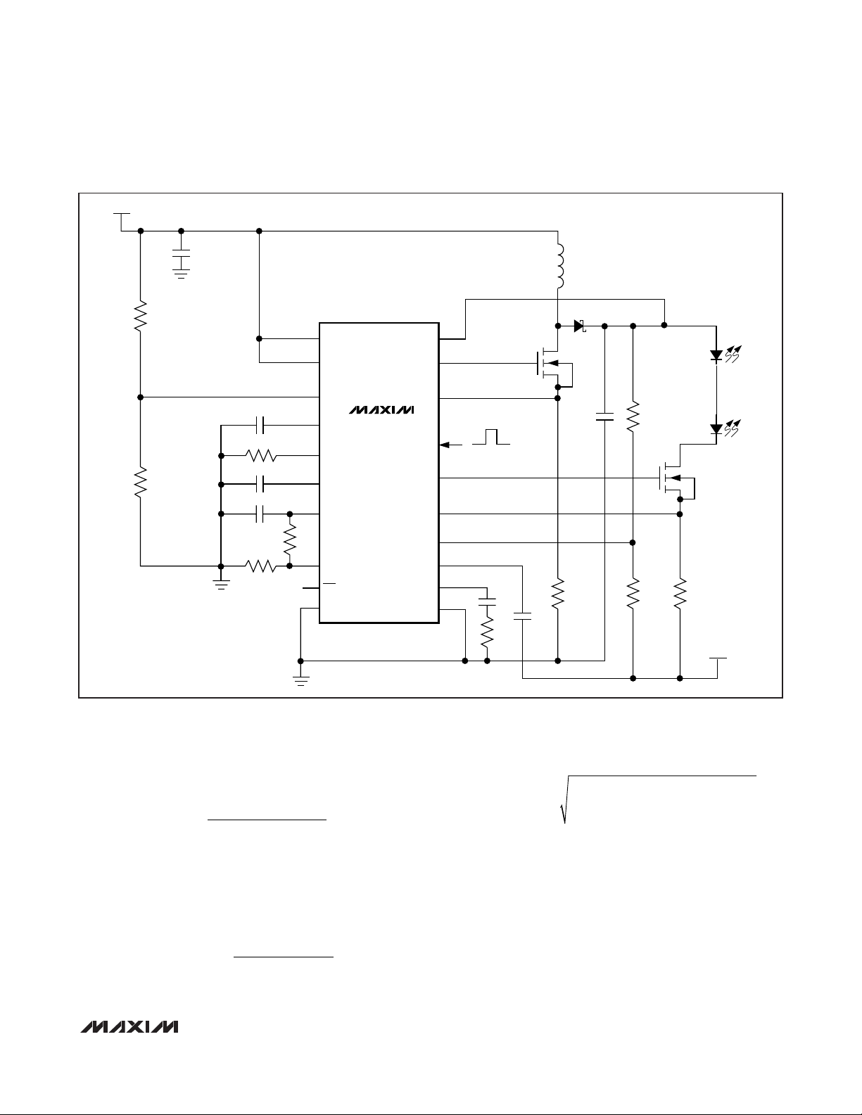
Boost Configuration
In the boost converter (Figure 2), the average inductor
current varies with the line voltage. The maximum average current occurs at the lowest line voltage. For the
boost converter, the average inductor current is equal
to the input current.
Calculate maximum duty cycle using the below equation.
where V
LED
is the forward voltage of the LED string in
volts, VDis the forward drop of the rectifier diode D1 in
volts (approximately 0.6V), V
INMIN
is the minimum input
supply voltage in volts, and V
FET
is the average drain to
source voltage of the MOSFET Q1 in volts when it is on.
Use an approximate value of 0.2V initially to calculate
D
MAX
. A more accurate value of the maximum duty
cycle can be calculated once the power MOSFET is
selected based on the maximum inductor current.
Use the following equations to calculate the maximum
average inductor current IL
AVG
, peak-to-peak inductor
current ripple ∆IL, and the peak inductor current ILPin
amperes:
Figure 2. Boost LED Driver
V
IN
C1
L1
R1
LV
IN
UVEN
C2
R3
C5
R2
C4
R5
HV
MAX16834
SC
RT/SYNC
V
CC
REF
R6
REFI
SGND
FLT
NDRV
CS
PWMDIM
DIMOUT
SENSE+
OVP+
CLV
COMP
PGND
Q1
ON
OFF
C7
R7
D1
C3
R4
Q2
R8
C6
R9
LED+
LEDs
LED-
R10
VVV
+−
LED D
=
VVV
+−
LEDDFET
D
MAX
INMIN
I
IL
AVG
LED
=
D
−1
MAX
Page 12

MAX16834
High-Power LED Driver with Integrated High-Side LED
Current Sense and PWM Dimming MOSFET Driver
12 ______________________________________________________________________________________
Allowing the peak-to-peak inductor ripple (∆IL) to be
±30% of the average inductor current:
and
The inductance value (L) of the inductor L1 in henries
(H) is calculated as:
where fSWis the switching frequency in hertz, V
INMIN
and V
FET
are in volts, and ∆IL is in amperes.
Choose an inductor that has a minimum inductance
greater than the calculated value. The current rating of
the inductor should be higher than ILPat the operating
temperature.
Buck-Boost Configuration
In the buck-boost LED driver (Figure 3), the average
inductor current is equal to the input current plus the
LED current.
Calculate maximum duty cycle using the below equation:
where V
LED
is the forward voltage of the LED string in
volts, VDis the forward drop of the rectifier diode D1
(approximately 0.6V) in volts, V
INMIN
is the minimum
input supply voltage in volts, and V
FET
is the average
drain to source voltage of the MOSFET Q1 in volts when
it is on. Use an approximate value of 0.2V initially to calculate D
MAX
. A more accurate value of maximum duty
cycle can be calculated once the power MOSFET is
selected based on the maximum inductor current.
Use the below equations to calculate the maximum
average inductor current IL
AVG
, peak-to-peak inductor
current ripple ∆IL, and the peak inductor current ILPin
amperes:
Allowing the peak-to-peak inductor ripple ∆I
L
to be
±30% of the average inductor current:
The inductance value (L) of the inductor L1 in henries is
calculated as:
where f
SW
is the switching frequency in hertz, V
INMIN
and V
FET
are in volts, and ∆IL is in amperes. Choose an
inductor that has a minimum inductance greater than
the calculated value.
Peak Current-Sense Resistor (R8)
The value of the switch current-sense resistor R8 for the
boost and buck-boost configurations is calculated as
follows:
where 0.25V is the minimum peak current-sense threshold, ILPis the peak inductor current in amperes, and
the factor 1.25 provides a 25% margin to account for
tolerances. The worst cycle-by-cycle current limiter triggers at 350mV (max). The I
SAT
of the inductor should
be higher than 0.35V/R8.
Output Capacitor
The function of the output capacitor is to reduce the
output ripple to acceptable levels. The ESR, ESL, and
the bulk capacitance of the output capacitor contribute
to the output ripple. In most applications, the output
ESR and ESL effects can be dramatically reduced by
using low-ESR ceramic capacitors. To reduce the ESL
and ESR effects, connect multiple ceramic capacitors
in parallel to achieve the required bulk capacitance. To
minimize audible noise generated by the ceramic
capacitors during PWM dimming, it may be necessary
to minimize the number of ceramic capacitors on the
output. In these cases an additional electrolytic or tantalum capacitor provides most of the bulk capacitance.
Boost and buck-boost configurations: The calculation of the output capacitance is the same for both
boost and buck-boost configurations. The output ripple
is caused by the ESR and the bulk capacitance of the
output capacitor if the ESL effect is considered negligible. For simplicity, assume that the contributions from
∆∆IIL
∆IIL
=××03 2.
LAVG
=××
LAVG
IL IL
=+
PAVG
03 2
.
I
L
2
IL IL
=+
PAVG
I
∆
L
2
VVD
()
L
=
−×
INMIN FET MAX
fI
×
∆
SW L
VV
+
D
=
MAX
VVV V
LED D INMIN FET
IL
AVG
LED D
++ −
I
LED
=
D
−1
MAX
VVD
()
L
=
−×
INMIN FET MAX
fI
×
∆
SW L
025
R
8
.
=
IL
(.)
P
×
125
Ω
Page 13
MAX16834
High-Power LED Driver with Integrated High-Side LED
Current Sense and PWM Dimming MOSFET Driver
______________________________________________________________________________________ 13
ESR and the bulk capacitance are equal, allowing 50%
of the ripple for the bulk capacitance. The capacitance
is given by:
where I
LED
is in amperes, C
OUT
is in farads, fSWis in
hertz, and ∆V
OUTRIPPLE
is in volts. The remaining 50%
of allowable ripple is for the ESR of the output capacitor. Based on this, the ESR of the output capacitor is
given by:
where IL
P
is the peak inductor current in amperes.
Use the below equation to calculate the RMS current
rating of the output capacitor:
Input Capacitor
The input filter capacitor bypasses the ripple current
drawn by the converter and reduces the amplitude of
high-frequency current conducted to the input supply.
The ESR, ESL, and the bulk capacitance of the input
capacitor contribute to the input ripple. Use a low-ESR
input capacitor that can handle the maximum input
RMS ripple current from the converter.
For the boost configuration, the input current is the
same as the inductor current. For buck-boost
Figure 3. Buck-Boost LED Driver (V
LED+
< 28V)
V
IN
C1
R1
LV
IN
C2
R3
C5
R2
C4
R5
UVEN
SC
MAX16834
RT/SYNC
V
CC
REF
R6
REFI
FLT
SGND
NDRV
PWMDIM
DIMOUT
SENSE+
OVP+
CLV
COMP
PGND
HV
Q1
CS
ON
OFF
C7
R7
L1
D1
C3
R8
C6
R4
Q2
R9
R10
LED+
LED-
V
LEDs
IN
ID
××
2
LED MAX
≥
Vf
∆
OUTRIPPLE SW
×
C
OUT
V
∆Ω()
<
OUTRIPPLE
IL
×
()2
P
ESR
COUT
(IL (1 D )) D
I
COUT(RMS)
=
AVG MAX
IL
+-(
VVG
A
××
××DD
MAX MAX
2
MAX
2
)( )
1-
Page 14

MAX16834
configuration, the input current is the inductor current
minus the LED current. But for both configurations, the
ripple current that the input filter capacitor has to supply is the same as the inductor ripple current with the
condition that the output filter capacitor should be connected to ground for buck-boost configuration. This
reduces the size of the input capacitor, as the inductor
current is continuous with maximum ±30% ripple.
Neglecting the effect of LED current ripple, the calculation of the input capacitor for boost as well as buckboost configurations is the same.
Neglecting the effect of the ESL, the ESR, and the bulk
capacitance at the input contributes to the input voltage
ripple. For simplicity, assume that the contribution from
the ESR and the bulk capacitance is equal. This allows
50% of the ripple for the bulk capacitance. The capacitance is given by:
where ∆ILis in amperes, CINis in farads, fSWis in hertz,
and ∆VINis in volts. The remaining 50% of allowable
ripple is for the ESR of the output capacitor. Based on
this, the ESR of the input capacitor is given by:
where ∆IL is in amperes, ESR
CIN
is in ohms, and ∆V
IN
is in volts.
Use the below equation to calculate the RMS current
rating of the input capacitor:
Slope Compensation
Slope compensation should be added to converters
with peak current-mode control operating in continuous
conduction mode with more than 50% duty cycle to
avoid current loop instability and subharmonic oscillations. The minimum amount of slope added to the peak
inductor current to stabilize the current control loop is
half of the falling slope of the inductor.
In the MAX16834, the slope compensating ramp is
added to the current-sense signal before it is fed to the
PWM comparator. Connect a capacitor (C2 in the application circuit) from SC to ground for slope compensation. This capacitor is charged with a 100µA current
source and discharged at the beginning of each switching cycle to generate the slope compensation ramp.
The value of the slope compensation capacitor C2 is
calculated as shown below:
Boost configuration:
where C2 is in farads, L is the inductance of the inductor L1 in henries, 100µA is the pullup current from SC,
V
LED
and V
INMIN
are in volts, and R8 is the switch cur-
rent-sense resistor in ohms.
Buck-boost configuration:
where C2 is in farads, L is the inductance of the inductor L1 in henries, 100µA is the pullup current from SC,
V
LED
is in volts, and R8 is the switch current-sense
resistor in ohms.
Selection of Power Semiconductors
Switching MOSFET
The switching MOSFET (Q1) should have a voltage rating sufficient to withstand the maximum output voltage
together with the diode drop of the rectifier diode D1
and any possible overshoot due to ringing caused by
parasitic inductances and capacitances. Use a
MOSFET with a drain-to-source voltage rating higher
than that calculated by the following equations:
Boost configuration:
where VDSis the drain-to-source voltage in volts and
VDis the forward drop of the rectifier diode D1. The factor of 1.2 provides a 20% safety margin.
Buck-boost configuration:
where VDSis the drain-to-source voltage in volts and
VDis the forward drop of the rectifier diode D1. The factor of 1.2 provides a 20% safety margin.
The continuous drain current rating of the selected
MOSFET, when the case temperature is at +70°C,
should be greater than the value calculated by the fol-
High-Power LED Driver with Integrated High-Side LED
Current Sense and PWM Dimming MOSFET Driver
14 ______________________________________________________________________________________
I
∆
C
≥
IN
ESR
CIN
I
CIN(RMS)
L
Vf
××
∆4
IN SW
V
∆
IN
<
I
×
∆ 2
L
∆I
L
=
3
2
-
L
×× ×
C2
C2
3 100 10
=
(V - V ) R8
LED INMIN
L
×× ×
3 100 10
=
(V ) R8
××
LED
6
××
2
-
6
2
VVV
=+
()
DS LED D
×12.
VVV V
=+ +
()
DS LED INMAX D
×12.
Page 15

lowing equation. The MOSFET must be mounted on a
board as per manufacturer specifications to dissipate
the heat.
The RMS current rating of the switching MOSFET Q1 is
calculated as follows for boost and buck-boost configurations:
where ID
RMS
is the MOSFET Q1’s drain RMS current in
amperes.
The MOSFET Q1 will dissipate power due to both
switching losses as well as conduction losses. The conduction losses in the MOSFET is calculated as follows:
where R
DSON
is the on-resistance of Q1 in ohms with
an assumed junction temperature of +100°C, P
COND
is
in watts, and IL
AVG
is in amperes.
Use the following equations to calculate the switching
losses in the MOSFET:
Boost configuration:
Buck-boost configuration:
where IGONand IG
OFF
are the gate currents of the
MOSFET Q1 in amperes when it is turned on and
turned off, respectively, V
LED
and V
INMAX
are in volts,
IL
AVG
is in amperes, fSWis in hertz, and CGDis the
gate-to-drain MOSFET capacitance in farads.
Choose a MOSFET that has a higher power rating than
that calculated by the following equation when the
MOSFET case temperature is at +70°C:
Rectifier Diode
Use a Schottky diode as the rectifier (D1) for fast
switching and to reduce power dissipation. The selected Schottky diode must have a voltage rating 20%
above the maximum converter output voltage. The maximum converter output voltage is V
LED
in boost configu-
ration and V
LED
+ V
INMAX
in buck-boost configuration.
The current rating of the diode should be greater than
I
D
in the following equation:
Dimming MOSFET
Select a dimming MOSFET (Q2) with continuous current
rating at +70°C, higher than the LED current by 30%.
The drain-to-source voltage rating of the dimming
MOSFET must be higher than V
LED
by 20%.
Feedback Compensation
The LED current control loop comprising of the switching converter, the LED current amplifier, and the error
amplifier should be compensated for stable control of
the LED current. The switching converter small-signal
transfer function has a right half-plane (RHP) zero for
both boost and buck-boost configurations as the inductor current is in continuous conduction mode. The RHP
zero adds a 20dB/decade gain together with a 90°
phase lag, which is difficult to compensate. The easiest
way to avoid this zero is to roll off the loop gain to 0dB
at a frequency less than one-fifth of the RHP zero frequency with a -20dB/decade slope.
The worst-case RHP zero frequency (f
ZRHP
) is calculat-
ed as follows:
Boost configuration:
Buck-boost configuration:
where f
ZRHP
is in hertz, V
LED
is in volts, L is the induc-
tance value of L1 in henries (H), and I
LED
is in amperes.
The switching converter small-signal transfer function
also has an output pole for both boost and buck-boost
configurations. The effective output impedance that
determines the output pole frequency together with the
output filter capacitance is calculated as:
MAX16834
High-Power LED Driver with Integrated High-Side LED
Current Sense and PWM Dimming MOSFET Driver
______________________________________________________________________________________ 15
ID IL D
⎛
=
()
⎜
RMS AVG MAX
⎝
×
⎞
×213.
⎟
⎠
2
××
PILDR
=
COND AVG MAX DSON
()
⎛
IL V C f
P
SW
AVG LED GD SW
=
⎜
⎝
⎛
11
×+
⎜
IG IG
⎝
ON OF
⎛
IL V V C f
×+ ××
()
P
SW
AVG LED INMAX GD SW
=
⎜
⎝
⎛
1
×
⎜
GGIG
I
⎝
ON OFF
1
+
2
×××
2
⎞
⎟
⎠
⎞
⎟
⎠
FF
2
2
⎞
⎟
⎠
⎞
⎟
⎠
PWP WPW
() () ()=+
TOT COND SW
IIL D
=× ×().115-
DAVG MAX
f
ZRHP
V
=
()12-
LED
××
2LI
π
MAX
LED
D
×
D
×
f
=
ZRHP
2LI
V
π
()12-
LED
×× ×
MAX
LED
D
MAX
Page 16

MAX16834
Boost configuration:
Buck-boost configuration:
where R
LED
is the dynamic impedance (rate of change
of voltage with current) of the LED string at the operating current, R10 is the LED current-sense resistor in
ohms, V
LED
is in volts, and I
LED
is in amperes.
The output pole frequency for both boost and buckboost configurations is calculated as follows:
where f
P2
is in hertz, C
OUT
is the output filter capaci-
tance in farads, R
OUT
is the effective output impedance
in ohms calculated above.
Compensation components R7 and C7 perform two
functions. C7 introduces a low-frequency pole that
introduces a -20dB/decade slope into the loop gain. R7
flattens the gain of the error amplifier for frequencies
above the zero formed by R7 and C7. For compensation, this zero is placed at the output pole frequency f
P2
such that it provides a -20dB/decade slope for frequencies above f
P2
for the complete loop gain.
The value of R7 needed to fix the total loop gain at f
P2
such that the total loop gain crosses 0dB at
-20dB/decade at one-fifth of the RHP zero can be calculated as follows:
where R7 is the compensation resistor in ohms, f
ZRHP
and fP2are in hertz, R8 is the switch current-sense
resistor in ohms, R10 is the LED current-sense resistor
in ohms, factor 9.9 is the gain of the LED current amplifier, and GM
COMP
is the transconductance of the error
amplifier in Siemens.
The value of C7 can be calculated as:
where C7 is in farads, f
P2
is in hertz, and R7 is in ohms.
To minimize switching frequency noise, an additional
capacitor can be added in parallel with the series combination of R7 and C7. The pole from this capacitor and
R7 must be a decade higher than the loop crossover
frequency.
Short-Circuit Protection
Boost Configuration
In the boost configuration (Figure 2), if the LED string is
shorted then the excess current flowing in the LED current-sense resistor will cause NDRV to stop switching.
The input voltage will appear on the output capacitor,
and this causes very high peak currents to flow in the
LED current-sense resistor R10 because the dimming
MOSFET (Q2) is on. Once the voltage across the LED
current-sense resistor exceeds 300mV for more than
5µs, then the dimming MOSFET Q2 turns off and stays
off for 4096 switching clock cycles. At the same time,
NDRV is also off. The MAX16834 goes into the hiccup
mode and recovers from hiccup once the short has
been removed. The power dissipation in the dimming
MOSFET (Q2) is minimized during a short across the
LED string. During the same period, FLT only goes high
when the dimming MOSFET is on.
Buck-Boost Configuration
In the case of the buck-boost configuration (Figure 3),
once an LED string short occurs then the behavior is
different. A short across the LED string causes a high
current spike due to the external capacitors at the output. The regulation loop will cause NDRV to stop
switching. This causes the voltage on HV to drop if its
voltage is derived from LED+. The voltage on CLV will
drop, and this drop is detected after 128 clock cycles.
The dimming MOSFET and the switching MOSFET will
stop switching. It stays off for 4096 clock cycles, and
the cycle repeats itself. The short across the LED string
will cause the MAX16834 to go into a hiccup mode. At
the same time the FLT signal asserts itself for 4096
clock cycles every hiccup cycle. In the case where the
HV voltage is derived from a source different than
LED+, then the LED current will stay in regulation even
during a short across the LED string. In this case, FLT
does not assert itself during the short.
High-Power LED Driver with Integrated High-Side LED
Current Sense and PWM Dimming MOSFET Driver
16 ______________________________________________________________________________________
R
OUT
()
=
RRIV
()
LED LED LED
10
LED LED
+×+
10
RRV
+×
R
=
OUT
RRID V
()
LED LED MAX
()
LED LED
+×× +
10
10
LLED
RRV
+×
1
××2π
CR
OUT OUT
=
f
P
2
fR
R
7
=
fDR GM
51 1099
××− × ××().
2
PMAX COMP
ZRHP
8
×
C
7
=
1
Rf
××2π
7
P
2
Page 17

MAX16834
High-Power LED Driver with Integrated High-Side LED
Current Sense and PWM Dimming MOSFET Driver
______________________________________________________________________________________ 17
Figure 4. Boost LED Driver with Automotive Load Dump Protection
V
IN
C1
L1
R1
D2
24V
R2
Q3
C8
C2
R3
C5
C4
R5
LV
IN
UVEN
HV
MAX16834
SC
RT/SYNC
V
CC
REF
R6
REFI
SGND
FLT
NDRV
CS
PWMDIM
DIMOUT
SENSE+
OVP+
CLV
COMP
PGND
Q1
ON
OFF
C7
R7
D1
C3
R4
Q2
R8
C6
R9
R10
LED+
LEDs
LED-
Page 18

MAX16834
High-Power LED Driver with Integrated High-Side LED
Current Sense and PWM Dimming MOSFET Driver
18 ______________________________________________________________________________________
Figure 5. High-Side Buck LED Driver
V
IN
LED+
C1
R1
R2
D1
LV
IN
UVEN
C2
SC
R3
C5
C4
R6
R5
RT/SYNC
V
CC
REF
REFI
FLT
SGND
MAX16834
NDRV
CS
PWMDIM
DIMOUT
SENSE+
OVP+
CLV
COMP
PGND
HV
Q1
ON
OFF
C7
C6
R7
V
LV
C3
L1
V
LV
R4
Q2
R8
R9
R10
LED-
V
LEDs
LV
Page 19

MAX16834
High-Power LED Driver with Integrated High-Side LED
Current Sense and PWM Dimming MOSFET Driver
______________________________________________________________________________________ 19
Figure 6. Boost DC-DC Converter
V
IN
C1
L1
V
R1
LV
FLT
D1
OUT
C2
R3
C5
R2
C4
R5
IN
UVEN
HV
MAX16834
SC
RT/SYNC
V
CC
REF
R6
REFI
SGND
NDRV
CS
PWMDIM
DIMOUT
SENSE+
OVP+
CLV
COMP
PGND
V
REF
Q1
C3 R4
R10
C6
R8
R7
OPTIONAL
R9
Page 20

MAX16834
High-Power LED Driver with Integrated High-Side LED
Current Sense and PWM Dimming MOSFET Driver
20 ______________________________________________________________________________________
Figure 7. Buck-Boost DC-DC Converter
V
IN
C1
L1
R1
R2
LV
IN
C2
R3
C5
C4
R5
UVEN
SC
MAX16834
RT/SYNC
V
CC
REF
R6
REFI
FLT
SGND
HV
NDRV
CS
PWMDIM
DIMOUT
SENSE+
OVP+
CLV
COMP
PGND
Q1
V
REF
N.C.
C6
R7
D1
C3 R4
R9
R8
R11
R10
V
OUT
V
IN
Page 21

MAX16834
High-Power LED Driver with Integrated High-Side LED
Current Sense and PWM Dimming MOSFET Driver
______________________________________________________________________________________ 21
Layout Recommendations
Typically, there are two sources of noise emission in a
switching power supply: high di/dt loops and high dv/dt
surfaces. For example, traces that carry the drain current often form high di/dt loops. Similarly, the heatsink
of the MOSFET connected to the device drain presents
a dv/dt source; therefore, minimize the surface area of
the heatsink as much as is compatible with the MOSFET power dissipation or shield it. Keep all PCB traces
carrying switching currents as short as possible to minimize current loops. Use ground planes for best results.
Careful PCB layout is critical to achieve low switching
losses and clean, stable operation. Use a multilayer
board whenever possible for better noise immunity and
power dissipation. Follow these guidelines for good
PCB layout:
1) Use a large contiguous copper plane under the
MAX16834 package. Ensure that all heat-dissipating components have adequate cooling.
2) Isolate the power components and high-current
path from the sensitive analog circuitry.
3) Keep the high-current paths short, especially at the
ground terminals. This practice is essential for stable, jitter-free operation. Keep switching loops short
such that:
a) The anode of D1 must be connected very close
to the drain of the MOSFET Q1.
b) The cathode of D1 must be connected very
close to C
OUT
.
c) C
OUT
and the current-sense resistor R8 must
be connected directly to the ground plane.
4) Connect PGND and SGND to a star-point configuration.
5) Keep the power traces and load connections short.
This practice is essential for high efficiency. Use
thick copper PCBs (2oz vs. 1oz) to enhance fullload efficiency.
6) Route high-speed switching nodes away from the
sensitive analog areas. Use an internal PCB layer
for the PGND and SGND plane as an EMI shield to
keep radiated noise away from the device, feedback dividers, and analog bypass capacitors.
7) To prevent discharge of the compensation capacitors during the off-time of the dimming cycle,
ensure that the PCB area close to these components has extremely low leakage. Discharge of
these capacitors due to leakage results in reduced
performance of the dimming circuitry.
Page 22

MAX16834
High-Power LED Driver with Integrated High-Side LED
Current Sense and PWM Dimming MOSFET Driver
Maxim cannot assume responsibility for use of any circuitry other than circuitry entirely embodied in a Maxim product. No circuit patent licenses are
implied. Maxim reserves the right to change the circuitry and specifications without notice at any time.
22
____________________Maxim Integrated Products, 120 San Gabriel Drive, Sunnyvale, CA 94086 408-737-7600
© 2008 Maxim Integrated Products is a registered trademark of Maxim Integrated Products, Inc.
Package Information
For the latest package outline information and land patterns, go
to www.maxim-ic.com/packages
.
PACKAGE TYPE PACKAGE CODE DOCUMENT NO.
20-TQFN-EP T2044-3
21-0139
MAX16834
TQFN
TOP VIEW
19
20
18
17
7
6
8
SGND
REF
REFI
9
OVP+
V
CC
PGND
CS
IN
1+2
DIMOUT
45
15 14 12 11
LV
SENSE+
UVEN
RT/SYNC
FLT
SC
COMP
NDRV
3
13
CLV
16
*EP
*EP = EXPOSED PAD.
10
PWMDIM
HV
Pin Configuration
Chip Information
PROCESS: BiCMOS–DMOS
 Loading...