

Page 1
General Description
The MAX16832A/MAX16832C step-down constant-current high-brightness LED (HB LED) drivers provide a
cost-effective design solution for automotive
interior/exterior lighting, architectural and ambient lighting, LED bulbs, and other LED illumination applications.
The MAX16832A/MAX16832C operate from a +6.5V to
+65V input voltage range. A high-side current-sense
resistor adjusts the output current up to 700mA, and a
dedicated pulse-width modulation (PWM) input
enables pulsed LED dimming over a wide range of
brightness levels.
These devices are well suited for applications requiring
a wide input voltage range. The high-side current sensing and an integrated current-setting circuitry minimize
the number of external components while delivering an
average output current with ±3% accuracy. A hysteretic
control method ensures excellent input supply rejection
and fast response during load transients and PWM dimming. The MAX16832A allows 10% current ripple, and
the MAX16832C allows 30% current ripple. Both
devices operate up to a 2MHz switching frequency,
thus allowing the use of small-sized components.
The MAX16832A/MAX16832C offer an analog dimming
feature that reduces the output current by applying an
external DC voltage below the internal 2V threshold voltage from TEMP_I to GND. TEMP_I also sources 25µA to
a negative temperature coefficient (NTC) thermistor connected between TEMP_I and GND, thus providing an
analog thermal-foldback feature that reduces the LED
current when the temperature of the LED string exceeds
a specified temperature point. Additional features
include thermal-shutdown protection.
The MAX16832A/MAX16832C operate over the -40°C to
+125°C automotive temperature range and are available
in a thermally enhanced 8-pin SO package.
Applications
Architectural, Industrial, and Ambient Lighting
Automotive RCL, DRL, and Fog Lights
Heads-Up Displays
Indicator and Emergency Lighting
MR16 and MR111 LED Lights
Features
o High-Efficiency Solution
o 6.5V to 65V Input Voltage Range
o On-Board 65V, 0.45Ω Power MOSFET
o Hysteretic Control: Up to 2MHz Switching
Frequency
o ±3% LED Current Accuracy
o 200mV Current-Sense Reference
o Resistor-Programmable Constant LED Current
o Integrated High-Side Current Sense
o Thermal-Foldback Protection/Linear Dimming
o Thermal-Shutdown Protection
o Available in a Thermally Enhanced 8-Pin SO
Package
o -40°C to +125°C Operating Temperature Range
MAX16832A/MAX16832C
2MHz, High-Brightness LED Drivers with
Integrated MOSFET and High-Side Current Sense
________________________________________________________________
Maxim Integrated Products
1
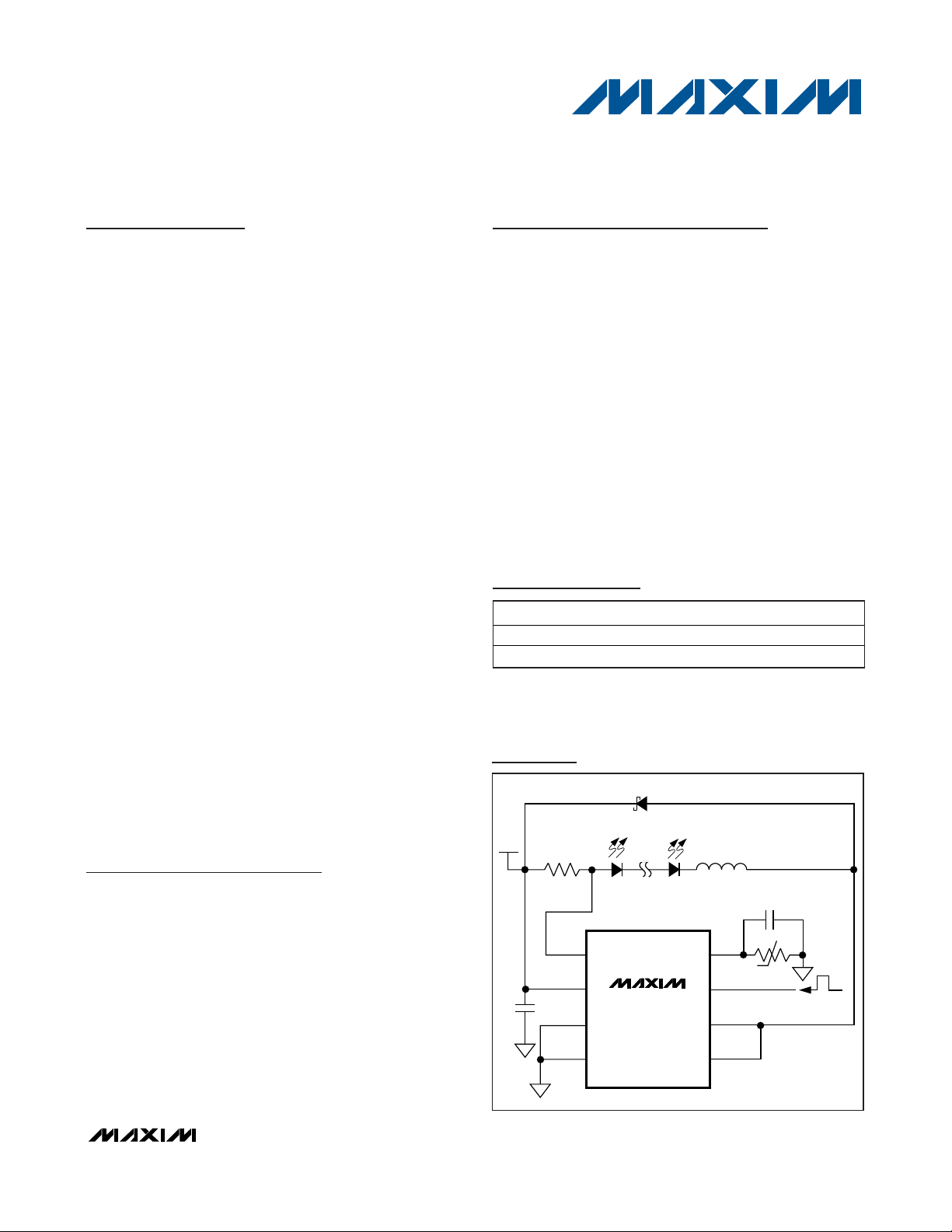
Ordering Information
LX
LXPGND
1
2
8
7
TEMP_I
DIMIN
GND
CS
3
4
6
5
MAX16832A
MAX16832C
L1
C2
ON
OFF
D1
HB LEDs
NTC
*
*
OPTIONAL
R
SENSE
V
IN
C1
Typical Application Circuit
19-4140; Rev 0; 5/08
For pricing, delivery, and ordering information, please contact Maxim Direct at 1-888-629-4642,
or visit Maxim’s website at www.maxim-ic.com.
+
Denotes a lead-free package.
*
Future product—contact factory for availability.
**
EP = Exposed pad.
PART TEMP RANGE
PIN-PACKAGE
MAX16832AASA+ -40°C to +125°C 8 SO-EP**
MAX16832CASA+*
-40°C to +125°C 8 SO-EP**
Pin Configuration appears at end of data sheet.
Page 2
MAX16832A/MAX16832C
2MHz, High-Brightness LED Drivers with
Integrated MOSFET and High-Side Current Sense
2 _______________________________________________________________________________________
ABSOLUTE MAXIMUM RATINGS
ELECTRICAL CHARACTERISTICS
(VIN= +24V, V
DIM
= VIN, TA= TJ= -40°C to +125°C, unless otherwise noted. Typical values are at TA = +25°C.)
Stresses beyond those listed under “Absolute Maximum Ratings” may cause permanent damage to the device. These are stress ratings only, and functional
operation of the device at these or any other conditions beyond those indicated in the operational sections of the specifications is not implied. Exposure to
absolute maximum rating conditions for extended periods may affect device reliability.
Note 1: Package thermal resistances were obtained using the method described in JEDEC specification JESD51-7, using a four-
layer board. For detailed information on package thermal considerations, refer to www.maxim-ic.com/thermal-tutorial
.
IN, CS, LX, DIM to GND .........................................-0.3V to +70V
TEMP_I to GND .......................................................-0.3V to +6V
PGND to GND ......................................................-0.3V to +0.3V
CS to IN .................................................................-0.3V to +0.3V
Maximum Current into Any Pin
(except IN, LX, and PGND).............................................20mA
Continuous Power Dissipation (T
A
= +70°C)
8-Pin SO (derate 23.3mW/°C above +70°C)...........1860.5mW
Junction-to-Ambient Thermal Resistance (θ
JA
) (Note 1) .....43°C/W
Operating Temperature Range .........................-40°C to +125°C
Junction Temperature......................................................+150°C
Storage Temperature Range .............................-65°C to +150°C
Lead Temperature (soldering, 10s) .................................+300°C
Pin-to-Pin ESD Ratings......................................................±2.5kV
Input Voltage Range V
Ground Current No switching 1.5 mA
Supply Current V
UNDERVOLTAGE LOCKOUT (UVLO)
Undervoltage Lockout UVLO
Undervoltage-Lockout Hysteresis 0.5 V
SENSE COMPARATOR
Sense Voltage Threshold High V
Sense Voltage Threshold Low V
Propagation Delay to Output High t
Propagation Delay to Output Low t
CS Input Current I
INTERNAL MOSFET
Drain-to-Source Resistance R
LX Leakage Current I
PARAMETER SYMBOL CONDITIONS MIN TYP MAX UNITS
IN
DIM
VCS = VIN - 100mV, VIN rising until VLX <
0.5V
V
CS
0.5V
MAX16832A, VIN - VCS rising from 140mV
SNSHI
SNSLO
DPDH
DPDL
CSIN
DSON
LX_LEAKVDIM
until V
MAX16832C, VIN - VCS rising from 140mV
until V
MAX16832A, VIN - VCS falling from 260mV
until V
MAX16832C, VIN - VCS falling from 260mV
until V
Falling edge of VIN - VCS from 140mV to
260mV to V
Rising edge of VCS - VIN from 260mV to
140mV to V
VIN - VCS = 200mV, VIN = V
VIN = V
I
LX
VIN = V
I
LX
< 0.6V, VIN = 12V 350 µA
IN
= VIN - 100mV, VIN falling until VLX >
IN
> 0.5VIN, V
LX
> 0.5VIN, V
LX
< 0.5VIN , V
LX
< 0.5VIN, V
LX
= 0.5V
LX
< 0.5V
LX
= 24V, VCS = 23.9V,
DIM
= 700mA
= 6.0V, VCS = 5.9V,
DIM
= 700mA
= 0V, VLX = 65V 10 µA
DIM
DIM
DIM
DIM
IN
IN
= 5V
= 5V
= 5V
= 5V
CS
6.5 65 V
201 210 216
218 230 236
185 190 198
166 170 180
6.25 6.5
6.0
50 ns
50 ns
3.5 µA
0.45 0.9
12
V
mV
mV
Ω
Page 3
MAX16832A/MAX16832C
2MHz, High-Brightness LED Drivers with
Integrated MOSFET and High-Side Current Sense
_______________________________________________________________________________________ 3
ELECTRICAL CHARACTERISTICS (continued)
(VIN= +24V, V
DIM
= VIN, TA= TJ= -40°C to +125°C, unless otherwise noted. Typical values are at TA = +25°C.)
EFFICIENCY
vs. INPUT VOLTAGE
MAX16832A toc01
VIN (V)
EFFICIENCY (%)
5545352515
75
80
85
90
95
100
70
565
1 LED
3 LEDs
5 LEDs
7 LEDs
9 LEDs
11 LEDs 13 LEDs
15 LEDs
9 LEDs
DUTY CYCLE
vs. INPUT VOLTAGE
MAX16832A toc02
VIN (V)
DUTY CYCLE (%)
5545352515
10
20
30
40
50
60
70
80
90
100
0
565
1 LED
3 LEDs
5 LEDs
7 LEDs
15 LEDs
13 LEDs
11 LEDs
FREQUENCY
vs. INPUT VOLTAGE
MAX16832A toc03
VIN (V)
FREQUENCY (kHz)
5545352515
50
100
150
200
250
300
350
400
450
500
0
565
1 LED
3 LEDs
5 LEDs
7 LEDs
9 LEDs
11 LEDs
13 LEDs
15 LEDs
16 LEDs
Typical Operating Characteristics
(VIN= V
DIM
= 48V, R
SENSE
= 0.3Ω, L = 220µH (connected between IN and CS). Typical values are at TA= +25°C, unless otherwise
noted.)
DIM INPUT
DIM Input-Voltage High V
DIM Input-Voltage Low V
DIM Turn-On Time t
DIM Input Leakage High V
DIM Input Leakage Low V
THERMAL SHUTDOWN
Thermal-Shutdown Threshold Temperature rising +165
Thermal-Shutdown Threshold
Hysteresis
THERMAL FOLDBACK
Thermal-Foldback Enable
Threshold Voltage
Thermal-Foldback Slope FB
TEMP_I Output Bias Current I
PARAMETER SYMBOL CONDITIONS MIN TYP MAX UNITS
IH
IL
DIM_ON
V
TFB_ON
SLOPE
TEMP_I
VIN - V
VCS - VIN = 100mV 0.6 V
V
DIM
DIM
DIM
V
DIM
V
DIM
= 100mV 2.8 V
CS
rising edge to VLX < 0.5V
= V
IN
IN
= 0V -3 -1.5 0 µA
= 5V 1.9 2.0 2.12 V
= 5V 0.75 1/V
25 26.5 28 µA
200 ns
815µA
o
C
10
o
C
Page 4

MAX16832A/MAX16832C
2MHz, High-Brightness LED Drivers with
Integrated MOSFET and High-Side Current Sense
4 _______________________________________________________________________________________
Typical Operating Characteristics (continued)
((VIN= V
DIM
= 48V, R
SENSE
= 0.3Ω, L = 220µH (connected between IN and CS). Typical values are at TA= +25°C, unless otherwise
noted.)
1.05
1.04
1.03
1.02
CURRENT
1.01
LED
1.00
0.99
0.98
NORMALIZED I
0.97
0.96
0.95
NORMALIZED I
1 LED
vs. INPUT VOLTAGE
LED
7 LEDs
5 LEDs
3 LEDs
VIN (V)
CURRENT
13 LEDs
11 LEDs
9 LEDs
QUIESCENT CURRENT
vs. INPUT VOLTAGE
500
450
400
MAX16832A toc04
350
300
15 LEDs
60555045403530252015105065
250
200
150
QUIESCENT CURRENT (μA)
100
50
0
065
VIN (V)
MAX16832A toc05
V
= 0V
DIM
605545 5015 20 25 30 35 405 10
PWM DIMMING
AT 200Hz (10% DUTY CYCLE)
1ms/div
MAX16832A toc06
V
IN
8 LEDs
= 48V
I
LED
200mA/div
0
V
DIM
5V/div
0
PWM DIMMING
AT 200Hz (90% DUTY CYCLE )
MAX16822A toc07
I
LED
200mA/div
0
V
DIM
IN
= 48V
5V/div
0
MAX16832A toc09
2.8
800
750
700
650
600
550
500
450
400
350
300
LED CURRENT (mA)
250
200
150
100
50
0
0
1ms/div
LED CURRENT
vs. V
TEMP_I
1.2
1.60.80.4
V
(V)
TEMP_I
V
8 LEDs
2.4
2.0
(A)
I
LED
PWM DIMMING
AT 20kHz (90% DUTY CYCLE)
10μs/div
I
LED
MAX16832A toc08
I
LED
200mA/div
0
V
DIM
5V/div
0
V
= 48V
IN
8 LEDs
vs. TEMPERATURE
1.0
0.9
0.8
0.7
0.6
0.5
0.4
0.3
0.2
0.1
VIN = 48V
0
TEMPERATURE (°C)
MAX16832A toc10
1109580655035205-10-25-40 125
Page 5

MAX16832A/MAX16832C
2MHz, High-Brightness LED Drivers with
Integrated MOSFET and High-Side Current Sense
_______________________________________________________________________________________
5
Typical Operating Characteristics (continued)
((VIN= V
DIM
= 48V, R
SENSE
= 0.3Ω, L = 220µH (connected between IN and CS). Typical values are at TA= +25°C, unless otherwise
noted.)
Pin Description
Detailed Description
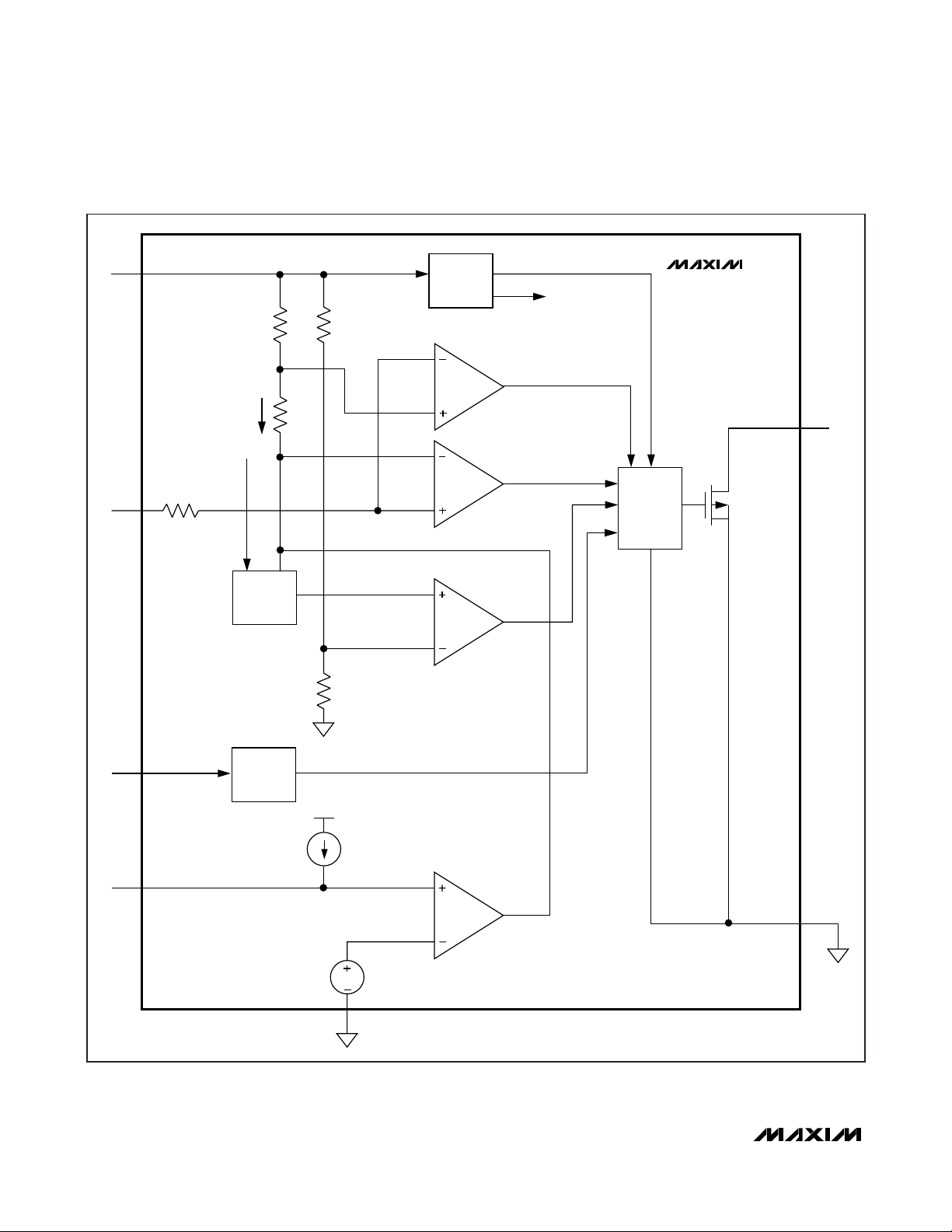
The MAX16832A/MAX16832C are step-down, constantcurrent, HB LED drivers. These devices operate from a
+6.5V to +65V input voltage range and deliver up to
700mA of output current. A high-side current-sense
resistor sets the output current and a dedicated PWM
dimming input enables pulsed LED dimming over a wide
range of brightness levels.
A high-side current-sensing scheme and an on-board
current-setting circuitry minimize the number of external components while delivering LED current with ±3%
accuracy, using a 1% sense resistor. See Figure 1 for
an internal block diagram.
0.7
0.6
0.5
(Ω)
0.4
RDSON
LX
0.3
0.2
0.1
-40 125
LX
RDSON
vs. TEMPERATURE
VIN = 65V
VIN = 48V
VIN = 6.5V
TEMPERATURE (°C)
30.0
29.5
MAX16832A toc11
1109580655035205-10-25
29.0
28.5
28.0
(μA)
27.5
TEMP_I
I
27.0
26.5
26.0
25.5
25.0
VIN = 48V
I
TEMP_I
vs. TEMPERATURE
TEMPERATURE (°C)
PIN NAME FUNCTION
1 CS Current-Sense Input. Connect a resistor between IN and CS to program the LED current.
2 IN Positive Supply Voltage Input. Bypass with a 1µF or higher value capacitor to GND.
3 GND Ground
4 PGND Power Ground
5, 6 LX Switching Node
7 DIM
8 TEMP_I
—EP
Logic-Level Dimming Input. Drive DIM low to turn off the current regulator. Drive DIM high to
enable the current regulator.
Thermal Foldback Control and Linear Dimming Input. Bypass with a 0.01µF capacitor to GND if
thermal foldback or analog dimming is used. See the Thermal Foldback section.
Exposed Pad. Connect EP to a large-area ground plane for effective power dissipation. Do not use
as the IC ground connection.
MAX16832A toc12
1109580655035205-10-25-40 125
Page 6
MAX16832A/MAX16832C
2MHz, High-Brightness LED Drivers with
Integrated MOSFET and High-Side Current Sense
6 _______________________________________________________________________________________
Figure 1. Internal Block Diagram
IN
I
SET
_ANA
V
CC
CS
BANDGAP
REF
1.23V
V
REGULATOR
CC
OPEN LED
COMPARATOR
CURRENT-SENSE
COMPARATOR
UVLO
COMPARATOR
V
MAX16832A
CC
_ANA
PWM
DIMMING
GATE
DRIVER
MAX16832C
LX
0.45Ω, 65V
DMOS SWITCH
DIM
TEMP_I
DIM
BUFFER
V
FTBON_THR
VCC _ANA
25μA
THERMAL
FOLDBACK
COMPARATOR
2V
GND
PGND
Page 7

Undervoltage Lockout (UVLO)
The MAX16832A/MAX16832C include a UVLO with
500mV hysteresis. The internal MOSFET turns off when
V
IN
falls below 5.5V to 6.0V.
DIM Input
LED dimming is achieved by applying a PWM signal at
DIM. A logic level below 0.6V at DIM forces the
MAX16832A/MAX16832Cs’ output low, thus turning off
the LED current. To turn the LED current on, the logic
level at DIM must be greater than 2.8V.
Thermal Shutdown
The MAX16832A/MAX16832C thermal-shutdown feature
turns off the LX driver when the junction temperature
exceeds +165°C. The LX driver turns back on when the
junction temperature drops 10°C below the shutdown
temperature threshold.
Analog Dimming
The MAX16832A/MAX16832C offer an analog-dimming
feature that reduces the output current when the voltage at TEMP_I is below the internal 2V threshold voltage. The MAX16832A/MAX16832C achieve analog
dimming by either an external DC voltage source connected between TEMP_I and ground or by a voltage on
a resistor connected across TEMP_I and ground
induced by an internal current source of 25µA. When
the voltage at TEMP_I is below the internal 2V threshold
limit, the MAX16832A/MAX16832C reduce the LED current. Use the following formula to set the analog dimming current:
where V
TFB_ON
= 2V and FB
SLOPE
= 0.75 are obtained
from the
Electrical Characteristics
table and VADis the
voltage at TEMP_I.
Thermal Foldback
The MAX16832A/MAX16832C include a thermal-foldback feature that reduces the output current when the
temperature of the LED string exceeds a specified temperature point. These devices enter thermal-foldback
mode when the voltage drop on the NTC thermistor,
thermally attached to the LEDs and electrically connected between TEMP_I and ground, drops below the
internal 2V threshold limit.
Applications Information
Selecting R
SENSE
to Set LED Current
The LED current is programmed with a current-sense
resistor connected between IN and CS. Use the following equation to calculate the value of this resistor:
where V
SNSHI
is the sense voltage threshold high and
V
SNSLO
is the sense voltage threshold low (see the
Electrical Characteristics
table for values).
Current-Regulator Operation
The MAX16832A/MAX16832C regulate the LED current
using a comparator with hysteresis (see Figure 2). As
the current through the inductor ramps up and the voltage across the sense resistor reaches the upper
threshold, the internal MOSFET turns off. The internal
MOSFET turns on again when the inductor current
ramps down through the freewheeling diode until the
voltage across the sense resistor equals the lower
threshold. Use the following equation to determine the
operating frequency:
where n is the number of LEDs, V
LED
is the forward
voltage drop of 1 LED, and ΔV = (V
SNSHI
- V
SNSLO
).
Inductor Selection
The MAX16832A/MAX16832C operate up to a switching frequency of 2MHz. For space-sensitive applications, the high switching frequency allows the size of
the inductor to be reduced. Use the following formula to
calculate an approximate inductor value and use the
closest standard value:
For component selection, use the MAX16832A/C Design
Tool available at: www.maxim-ic.com/MAX16832-
software.
MAX16832A/MAX16832C
2MHz, High-Brightness LED Drivers with
Integrated MOSFET and High-Side Current Sense
_______________________________________________________________________________________ 7
IAI A FB
() () ()
=×
TF LED SLOPE TFB ON AD
⎡
−−1
⎢
⎣
1
⎛
⎞
VVV
×
⎜
⎟
()
⎝
⎠
V
_
R
SENSE
()
Ω=
2
−()
VnV nV R
f
SW
⎤
⎥
⎦
L approx
(.)
IN LED LED SENSE
=
−
VnV nV R
()
IN LED LED SENSE
=
VVV
()()
VVL
IN
+1
SNSHI SNSLO
IA
()
LED
××
Δ
××
××
Δ
VVf
××
IN SW
Page 8

MAX16832A/MAX16832C
2MHz, High-Brightness LED Drivers with
Integrated MOSFET and High-Side Current Sense
8 _______________________________________________________________________________________
Freewheeling-Diode Selection
For stability and best efficiency, a low forward-voltage
drop diode with fast reverse-recovery time and low
capacitance is recommended. A Schottky diode is a
good choice as long as its breakdown voltage is high
enough to withstand the maximum operating voltage.
PCB Layout Guidelines
Careful PCB layout is critical to achieve low switching
losses and stable operation. Use a multilayer board
whenever possible for better noise immunity. Minimize
ground noise by connecting high-current ground
returns, the input bypass-capacitor ground lead, and
the output-filter ground lead to a single point (star
ground configuration). In normal operation, there are two
power loops. One is formed when the internal MOSFET
is on and the high current flows through IN, R
SENSE
,
LED load, the inductor, the internal MOSFET, and GND.
The other loop is formed when the internal MOSFET is
off and the high current circulates through R
SENSE
, LED
load, the inductor, and the freewheeling diode. Minimize
each loop area to reduce noise interaction.
Place R
SENSE
as close as possible to CS and IN. For
better noise immunity, a Kelvin connection between CS
and R
SENSE
is strongly recommended.
Due to the integrated power MOSFET, the SO-EP package has an exposed pad to transfer the heat from the
chip to the PCB. To make the thermal resistance
between the chip and PCB lower, the exposed pad
must be soldered to the PCB. The exposed pad is connected to GND.
Figure 2. Current-Regulator Operation
HYSTERETIC
MODE
f
I
LED
AVG. LED
CURRENT
V
DIM
SW
ΔI
t
t1
tt2
Page 9

MAX16832A/MAX16832C
2MHz, High-Brightness LED Drivers with
Integrated MOSFET and High-Side Current Sense
Maxim cannot assume responsibility for use of any circuitry other than circuitry entirely embodied in a Maxim product. No circuit patent licenses are
implied. Maxim reserves the right to change the circuitry and specifications without notice at any time.
Maxim Integrated Products, 120 San Gabriel Drive, Sunnyvale, CA 94086 408-737-7600 _____________________
9
© 2008 Maxim Integrated Products is a registered trademark of Maxim Integrated Products, Inc.
Chip Information
PROCESS: BiCMOS
Package Information
For the latest package outline information, go to
www.maxim-ic.com/packages
.
PACKAGE TYPE PACKAGE CODE DOCUMENT NO.
8 SO-EP S8E-12
21-0111
LX
LXPGND
1
2
8
+
7
TEMP_I
DIMIN
GND
CS
SO-EP
TOP VIEW
3
4
6
5
MAX16832A
MAX16832C
Pin Configuration
 Loading...