

Page 1
General Description
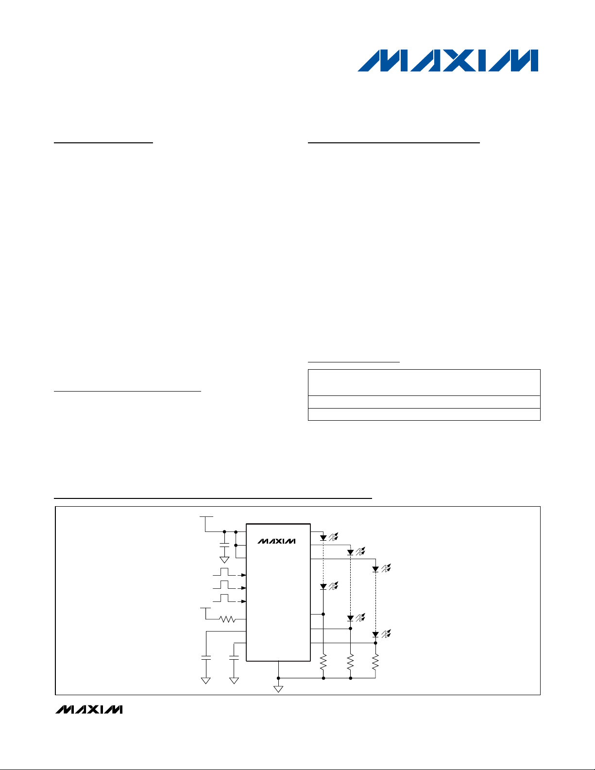
The MAX16823 three-channel LED driver operates from a
5.5V to 40V input voltage range and delivers up to 70mA
per channel to one or more strings of high-brightness
LEDs (HBLEDs). Each channel’s current is programmable
using an external current-sense resistor in series with the
LEDs. Three DIM inputs allow a wide range of independent pulsed dimming in addition to providing the on and
off control of the outputs. Wave-shaping circuitry reduces
EMI while providing fast turn-on and turn-off times.
The MAX16823 is well suited for automotive applications
requiring a high-voltage input and is able to withstand
load-dump events up to 45V. On-board pass elements
minimize external components while providing ±5% LED
current accuracy. Additional features include an activehigh, open-drain LEDGOOD output for open LED detection, a +3.4V (±5%) regulated output with 4mA output
current capability, short-circuit and thermal protections.
The MAX16823 is available in thermally enhanced 5mm x
5mm, 16-pin TQFN-EP and 16–pin TSSOP-EP packages
and is specified over the -40°C to +125°C automotive
temperature range.
Applications
Automotive Exterior: Rear Combination Lights
(RCLs), CHMSL
Automotive Interior: RGB Ambient Lighting,
Cluster Lighting, and LCD Backlighting
Emergency Vehicle Warning Lights
Navigation and Marine Indicators
Architectural and Industrial Lighting
Features
5.5V to 40V Operating Range
Adjustable Constant Output Current
(5mA to 70mA and Up to 2A with External BJT)
±5% Output Current Accuracy
Open LED Detection
Three Independent High-Voltage DIM Inputs
Three Integrated Pass Elements with Low
Dropout Voltage (0.7V max)
Undervoltage Lockout
Output Short-Circuit Protection
3.4V Voltage Regulator with 4mA Capability
Accurate, Low 203mV Current Sense
Overtemperature Shutdown
-40°C to +125°C Operating Temperature Range
MAX16823
High-Voltage, 3-Channel Linear High-Brightness
LED Driver with Open LED Detection
________________________________________________________________
Maxim Integrated Products
1
Ordering Information
Typical Operating Circuit
19-0733; Rev 0; 1/07
For pricing, delivery, and ordering information, please contact Maxim/Dallas Direct! at
1-888-629-4642, or visit Maxim’s website at www.maxim-ic.com.
Pin Configurations appear at end of data sheet.
+
Denotes a lead-free package.
*
Future product—contact factory for availability.
**
EP = Exposed pad.
PART TEMP RANGE
MAX16823ATE+*
MAX16823AUE+ -40°C to +125°C 16 TSSOP-EP** U16E-3
-40°C to +125 °C 16 TQFN-EP** T1655-3
PINPACKAGE
PKG
CODE
V
IN
IN
C
IN
REG
R
LEDGOOD
C
C
LGC
REG
IN
IN
DIM1
DIM2
DIM3
LEDGOOD
LGC
REG
MAX16823
GND
OUT1
OUT2
OUT3
CS1
CS2
CS3
CS1 CS2 CS3
Page 2
MAX16823
High-Voltage, 3-Channel Linear High-Brightness
LED Driver with Open LED Detection
2 _______________________________________________________________________________________
ABSOLUTE MAXIMUM RATINGS
ELECTRICAL CHARACTERISTICS
(VIN= 12V, C
REG
= 0.1µF, I
REG
= 0, C
LGC
= 15nF, V
DIM1
= V
DIM2
= V
DIM3
= 3.4V, R
CS_
= 2.85Ω from CS_ to GND, TJ= TA = -40°C
to +125°C, unless otherwise noted. Typical values are at T
A
= +25°C.) (Note 1)
Stresses beyond those listed under “Absolute Maximum Ratings” may cause permanent damage to the device. These are stress ratings only, and functional
operation of the device at these or any other conditions beyond those indicated in the operational sections of the specifications is not implied. Exposure to
absolute maximum rating conditions for extended periods may affect device reliability.
IN to GND ...............................................................-0.3V to +45V
OUT1, OUT2, OUT3, DIM1, DIM2,
DIM3 to GND ...........................................-0.3V to (V
IN
+ 0.3V)
REG, LGC, LEDGOOD to GND ................................-0.3V to +6V
CS1, CS2, CS3 to GND .........................................-0.3V to +0.5V
OUT1, OUT2, OUT3 Short Circuited
to GND Duration (V
IN
+ 16V)..........................................60min
Maximum Current into Any Pin
(except IN, OUT1, OUT2, OUT3)..................................±20mA
Continuous Power Dissipation (T
A
= +70°C)
16-Pin TQFN 5mm x 5mm
(derate 33.3mW/°C above +70°C).........................2666mW
16-Pin TSSOP (derate 26.1mW/°C above +70°C) ....2088.8mW
Operating Temperature Range .........................-40°C to +125°C
Junction Temperature......................................................+150°C
Storage Temperature Range .............................-65°C to +150°C
Lead Temperature (soldering, 10s) .................................+300°C
Supply Voltage Range V
Undervoltage Lockout UVLO
Ground Current I
Guaranteed Output Current I
LED Current-Sense Accuracy 5mA ≤ I
Dropout Voltage (Note 2) ∆VDO
Output Current Slew Rate 8 mA/µs
Short-Circuit Current V
LEDGOOD
LEDGOOD Output Logic Low V
LGC Pullup Resistor 65 100 135 kΩ
LGC Input Upper Threshold V
LGC Input Lower Threshold V
LGC Pulldown Current V
LGC Clock Period C
DIMMING INPUT (DIM1, DIM2, DIM3)
DIM_ Logic-Input Bias Current I
DIM_ Input-Voltage High 2.4 V
DIM_ Input-Voltage Low 0.6 V
DIM_ Frequency 0 3 kHz
OUTPUTS (OUT1, OUT2, AND OUT3) (Note 3)
Turn-On Time DIM_ rising edge to 90% of OUT_ current 12 28 µs
Turn-Off Time DIM_ falling edge to 10% of OUT_ current 8 18 µs
Output Current Rise Time 10% to 90% 7 18 µs
Output Current Fall Time 90% to 10% 6 15 µs
PARAMETER SYMBOL CONDITIONS MIN TYP MAX UNITS
OUT
DIM_
IN
G
OL
UTH
LTH
VIN rising 4.4 4.9 5.4
falling 4.0 4.6 5.2
V
IN
I
= I
OUT1
OUT_
I
= 70mA, 6.5V ≤ VIN ≤ 40V 0.3 0.7
OUT_
I
= 70mA, 5.5V ≤ VIN ≤ 6.5V 0.3 0.8
OUT_
= 0V 180 mA
OUT_
I
= 2mA 0.4 V
SINK
> V
LGC
= 15nF 0.77 1.5 2.3 ms
LGC
5.5 40 V
= I
OUT2
≤ 70mA 5 %
UTH
= 70mA 1.5 3 mA
OUT3
70 mA
2.53 V
0.8 V
20 mA
-0.1 +0.1 µA
IN
V
V
V
Page 3
MAX16823
High-Voltage, 3-Channel Linear High-Brightness
LED Driver with Open LED Detection
_______________________________________________________________________________________ 3
Note 1: All devices 100% production tested at TJ= +25°C. Limits over the operating temperature range are guaranteed by design.
Note 2: Dropout is measured as follows: Connect a resistor from OUT_ to CS_. Connect R
CS_
= 2.85Ω from CS_ to GND.
Set V
IN
= V
OUT
+ 3V (record V
OUT
as V
OUTA
). Reduce VINuntil V
OUT
= 0.97 x V
OUTA
(record as V
INB
and V
OUTB
).
VDO = V
INB
- V
OUTB
.
Note 3: Output current rise and fall times are measured with a 62Ω series resistor from OUT_ to CS_.
Note 4: Overtemperature protection does not function if the output of the 3.4V reference (REG) is shorted to ground.
ELECTRICAL CHARACTERISTICS (continued)
(VIN= 12V, C
REG
= 0.1µF, I
REG
= 0, C
LGC
= 15nF, V
DIM1
= V
DIM2
= V
DIM3
= 3.4V, R
CS_
= 2.85Ω from CS_ to GND, TJ= TA = -40°C
to +125°C, unless otherwise noted. Typical values are at T
A
= +25°C.) (Note 1)
Typical Operating Characteristics
(VIN= 12V, C
REG
= 0.1µF, I
REG
= 0, V
LGC
= unconnected, connect R
CS_
= 2.85Ω from CS_ to GND. Connect OUT_ to CS_ through
a resistor, T
J
= -40°C to +125°C, unless otherwise noted. Typical values are at TA= +25°C.)
V
CS_
vs. OUTPUT CURRENT
OUTPUT CURRENT (mA)
V
CS_
(V)
MAX16823 toc02
0 10203040506070
0.200
0.201
0.202
0.203
0.204
0.205
0.206
0.207
0.208
0.209
0.210
OUTPUT CURRENT vs. INPUT VOLTAGE
INPUT VOLTAGE (V)
OUTPUT CURRENT (mA)
MAX16823 toc03
0 5 10 15 20 25 30 35 40
0
10
20
30
40
50
60
70
80
90
100
I
OUT
= 70mA
I
OUT
= 5mA
OUTPUT CURRENT vs. TEMPERATURE
TEMPERATURE (°C )
OUTPUT CURRENT (mA)
MAX16823 toc01
-40 -25 -10 5 20 35 50 65 80 95 110 125
0
10
20
30
40
50
60
70
80
90
100
I
LOAD
= 5mA
I
LOAD
= 35mA
I
LOAD
= 70mA
CURRENT SENSE
Regulated CS_ Voltage V
Input Current (CS1, CS2, CS3) Current out of CS_ +1.2 µA
OVERTEMPERATURE PROTECTION (Note 4)
Thermal Shutdown Temperature 155 °C
Thermal Shutdown Hysteresis 23 °C
3.4V REGULATOR (REG)
Output Voltage V
REG Short-Circuit Current V
PARAMETER SYMBOL CONDITIONS MIN TYP MAX UNITS
CS_
REG
5mA ≤ I
OUT
_ ≤ 70mA 193 203 213 mV
3.275 3.41 3.547
0 ≤ I
≤ 4mA 3.221 3.38 3.547
REG
= 0V 13 mA
REG
V
Page 4
MAX16823
High-Voltage, 3-Channel Linear High-Brightness
LED Driver with Open LED Detection
4 _______________________________________________________________________________________
Typical Operating Characteristics (continued)
(VIN= 12V, C
REG
= 0.1µF, I
REG
= 0, V
LGC
= unconnected, connect R
CS_
= 2.85Ω from CS_ to GND. Connect OUT_ to CS_ through
a resistor, T
J
= -40°C to +125°C, unless otherwise noted. Typical values are at TA= +25°C.)
DROPOUT VOLTAGE vs. TEMPERATURE
1.0
0.9
0.8
0.7
0.6
0.5
0.4
0.3
DROPOUT VOLTAGE (mV)
0.2
0.1
0
-40 -25 -10 5 20 35 50 65 80 95 110 125
SUPPLY CURRENT vs. TEMPERATURE
1.4
V
= V
= V
= 0V
DIM3
VIN = 40V
VIN = 5.5V
TEMPERATURE (°C)
I
= 70mA
LOAD
TEMPERATURE (°C)
1.3
MAX16823 toc04
1.2
1.1
1.0
0.9
SUPPLY CURRENT (mA)
0.8
0.7
0.6
DIM1
DIM2
VIN = 20V
VIN = 12V
-40-25-105 203550658095110125
MAX16823 toc05
(V)
V
V
vs. TEMPERATURE
3.5
3.4
3.3
REG
3.2
3.1
3.0
-40 -25 -10 5 20 35 50 65 80 95 110 125
REG
I
LOAD
I
= 4mA
LOAD
TEMPERATURE (°C)
= 0
I
LOAD
= 1mA
MAX16823 toc06
V
vs. I
CS_
0.210
0.209
0.208
0.207
0.206
0.205
0.204
(V)
0.203
0.202
CS_
V
0.201
0.200
0.199
0.198
0.197
0.196
0.195
012345678910
REG
I
= 70mA
LOAD
I
(mA)
REG
200Hz DIMMED OPERATION (EXPANDED)
I
LOAD
VIN = 12V, DIM
PULSED AT 200Hz
(50% DUTY CYCLE)
= 70mA
MAX16823 toc10
MAX16823 toc07
V
DIM
2V/div
0V
I
LOAD
50mA/div
0A
V
vs. V
3.45
3.44
3.43
3.42
3.41
(V)
3.40
REG
V
3.39
I
3.38
3.37
3.36
3.35
= 1mA
REG
0 5 10 15 20 25 30 35 40
REG
I
= 0
REG
IN
I
= 4mA
REG
V
(V)
IN
200Hz DIMMED OPERATION (EXPANDED)
I
LOAD
VIN = 12V, DIM
PULSED AT 200Hz
(50% DUTY CYCLE)
= 70mA
MAX16823 toc11
MAX16823 toc08
V
DIM
2V/div
0V
I
LOAD
50mA/div
0A
330Hz DIMMED OPERATION
I
VIN = 12V, DIM
PULSED AT 33Hz
(1% DUTY CYCLE)
20µs/div
LEDGOOD RESPONSE TIMES
LOAD
= 70mA
V
IN
C
LGC
MAX16823 toc09
MAX16823 toc12
= 12V
= 15nF
V
DIM
2V/div
0V
I
LED
50mA/div
0A
V
DIM
5V/div
0V
V
LEDGOOD
5V/div
0V
V
LGC
5V/div
0V
10µs/div
10µs/div
2ms/div
Page 5

MAX16823
High-Voltage, 3-Channel Linear High-Brightness
LED Driver with Open LED Detection
_______________________________________________________________________________________ 5
Pin Description
PIN
TQFN TSSOP
1 3 DIM1
2 4 DIM2
3 5 DIM3
4 6 LEDGOOD
5, 6, 7 7, 8, 9 IN
810LGC
9 11 REG 3.4V V ol tag e Reg ul ator . C onnect a 0.1µF cap aci tor fr om RE G to G N D .
10 12 GND G r ound
11 13 CS3
12 14 CS2
13 15 CS1
14 16 OUT3 C ur r ent Reg ul ator O utp ut 3
15 1 OUT2 C ur r ent Reg ul ator O utp ut 2
16 2 OUT1 C ur r ent Reg ul ator O utp ut 1
EP EP EP
NAME FUNCTION
D i m m i ng Inp ut 1. D IM 1 i s a l ow - fr eq uency d i m m i ng i np ut for channel 1. A l og i c- l ow tur ns off
O U T1 and a l og i c- hi g h tur ns on O U T1.
D i m m i ng Inp ut 2. D IM 2 i s a l ow - fr eq uency d i m m i ng i np ut for channel 2. A l og i c- l ow tur ns off
O U T2 and a l og i c- hi g h tur ns on O U T2.
D i m m i ng Inp ut 3. D IM 3 i s a l ow - fr eq uency d i m m i ng i np ut for channel 3. A l og i c- l ow tur ns off
O U T3 and a l og i c- hi g h tur ns on O U T3.
Open LED Output. LEDGOOD is an open-drain output. A logic-high indicates the LED
connection i s g ood i n al l thr ee channel s. A l og i c- l ow i nd i cates an op en LE D connecti on. S ee the
LE D GO OD secti on.
P osi ti ve Inp ut S up p l y. Byp ass w i th a 0.1µF ( m i n) cap aci tor to G N D . C onnect al l IN
p i ns tog ether .
LE D D etecti on- Ti m i ng S etti ng . C onnect a cap aci tor fr om LGC to g r ound to set the d el ay ti m e
for LE D G OO D .
C hannel 3 S ense Am p l i fi er P osi ti ve Inp ut. C onnect the cur r ent- sense r esi stor b etw een C S 3
and G N D to p r og r am the outp ut cur r ent l evel for channel 3.
C hannel 2 S ense Am p l i fi er P osi ti ve Inp ut. C onnect the cur r ent- sense r esi stor b etw een C S 2
and G N D to p r og r am the outp ut cur r ent l evel for channel 2.
C hannel 1 S ense Am p l i fi er P osi ti ve Inp ut. C onnect the cur r ent- sense r esi stor b etw een C S 1
and G N D to p r og r am the outp ut cur r ent l evel for channel 1.
E xp osed P ad . C onnect E P to a l ar g e- ar ea g r ound p l ane for effecti ve p ow er d i ssi p ati on. D o not
use as the IC g r ound connecti on.
Page 6

MAX16823
High-Voltage, 3-Channel Linear High-Brightness
LED Driver with Open LED Detection
6 _______________________________________________________________________________________
Detailed Description
The MAX16823 three-channel current regulator operates
from a 5.5V to 40V input voltage range and delivers up
to 70mA per channel to one or more strings of HBLEDs.
The output currents are programmable using external
current-sense resistors in series with the LEDs. Three
DIM inputs allow a wide range of independent pulsed
dimming in addition to providing the on and off control
of the outputs. The MAX16823 offers an LEDGOOD
output that indicates an open-circuit condition when
one or more LED channels are open.
Integrated pass elements minimize external components while providing ±5% output current accuracy.
Additional features include a 3.4V (±5%) voltage regulator with 4mA output current capability, short-circuit and
thermal protection.
The MAX16823 uses a feedback loop to linearly control
the current from each output. The voltage across each
sense resistor is compared to a fixed reference voltage
and the error is amplified to drive the internal power
pass device for a particular channel. See the
Block
Diagram
. The regulation point is factory-set at 203mV.
The regulated current is adjusted by the value of
R
CS__
.
The MAX16823 is a constant-current LED driver internally optimized for driving the impedance range
expected from one or more HBLEDs.
3.4V Regulator (REG)
The MAX16823 includes a fixed 3.4V voltage regulator
that delivers up to 4mA of load current for auxiliary
applications throughout the 5.5V to 40V input voltage
range. Connect a 0.1µF compensation capacitor from
REG to ground. Shorting REG to ground disables the
thermal shutdown.
Thermal Protection
The MAX16823 enters a thermal-shutdown mode in the
event of overheating. This typically occurs in overload or
output short-circuit conditions. When the junction temperature exceeds TJ= +155°C, the internal thermal protection circuitry turns off the series pass elements. The
MAX16823 recovers from thermal-shutdown mode once
the junction temperature drops by 23°C. The part will
therefore protect itself by low-frequency thermal cycling
in the event of a short-circuit or overload condition.
Applications Information
Programming the LED Current
The MAX16823 uses sense resistors to set the output
current for each channel. To set the LED current for a
particular channel, connect a sense resistor across the
corresponding current-sense input (CS_) and GND. For
optimal accuracy, connect the low-side of the currentsense resistors to the IC’s ground pin with short traces.
The value needed for the sense resistor for a given current can be calculated with the equation below:
where V
CS_
is 203mV and I
OUT_
is the desired LED
current (I
LED
).
Input-Voltage Considerations
For proper operation, the minimum input voltage must
always be:
where V
FT(MAX)
is the total forward voltage of all seriesconnected LEDs. The minimum operating voltage of
the device is 5.5V.
LEDGOOD
The MAX16823 features an active-low, open-drain
LEDGOOD output that goes low either when one or
more LED channels are open or when a signal at any of
the dimming inputs remains low for a period greater
than the programmed LEDGOOD delay time t
DELAY
.
Program t
DELAY
with a capacitor connected between
LGC and ground. The LEDGOOD output goes low after
the programmed delay period t
DELAY
has elapsed. Use
the following formula to set the delay period:
where C
LGC
is the capacitor connected between LGC
and ground. The LEDGOOD output goes low during
the thermal shutdown.
tCF
DELAY LGC
=×257 900,() ()Ω
VV V V
IN MIN CS MAX FT MAX DO MAX( ) _( ) ( ) ( )
≥ ++
R
VV
IA
CS
CS
OUT
_
_
_
()
()
()
Ω =
Page 7

MAX16823
High-Voltage, 3-Channel Linear High-Brightness
LED Driver with Open LED Detection
_______________________________________________________________________________________ 7
Pulse-Dimming Inputs (DIM_)
The MAX16823 features pulsed or chopped-current
dimming inputs (DIM_) to chop the LED current and to
adjust the brightness. DIM_ also serves as an activehigh enable input. A logic-low at DIM_ turns off OUT_
and a logic-high turns on OUT_. If the signal at DIM
stays low more than the programmed LEDGOOD delay
time, LEDGOOD goes low (Figure 1).
Two Brightness Levels for
TAIL/STOP Lights
Figure 2 shows the PWM dimming operation for the
MAX16823 with an ICM7555 timer. The ICM7555 provides an adjustable duty cycle using two external resistors and a capacitor. In TAIL operation, the output of
the ICM7555 feeds into DIM and lights up the LEDs.
The LED’s brightness depends on the duty cycle of the
Block Diagram
GND
DIM1
REG
UVLO
IN
IN
IN
IN
BANDGAP
MAX16823
THERMAL
SHUTDOWN
I_REG
OUT1
CS1
IN
I_REG
OUT2
DIM2
DIM3
LEDGGOOD
LGC
LEDGOOD
DETECTOR
CS2
IN
I_REG
OUT3
CS3
Page 8

MAX16823
High-Voltage, 3-Channel Linear High-Brightness
LED Driver with Open LED Detection
8 _______________________________________________________________________________________
ICM7555. When V
STOP
is present, DIM is pulled up to
V
STOP
. The PWM dimming operation is disabled and
the LEDs light up to full brightness. See the ICM7555
data sheet for formulas to calculate the dimming frequency and the duty cycle.
Outputs Latch-Off
Figure 3 shows a circuit with DIM1, DIM2, DIM3, and
LEDGOOD connected through a resistor to V
REG
. This
circuit is useful for applications that require all outputs
to latch off when one of the LEDs opens. The
MAX16823 resumes current regulation again through
power cycling, once the fault condition is removed.
Other Applications
The application circuit in Figure 4 implements a twolevel brightness current for TAIL/STOP lights. In TAIL
operation, Q1 is off and R
CS1
sets the output current. In
STOP operation, Q1 turns on and the output current is
set by a parallel combination of R
CS1
and R2.
Figure 5 shows an application circuit with the
MAX16823 using a single BJT to provide high output
current. For proper operation:
For minimized dropout, the LEDs can be placed in the
collector.
VV V VV
IN MIN BE MAX FT MAX CS DO MAX() () () _ ()
>+++
Figure 1. LEDGOOD Timing Delay
Figure 2. PWM Dimming Operation with ICM7555
DIM
LEDGOOD
t
ON
t
OFF
LEDGOOD GOES
LOW WHEN t
OFF
> t
DELAY
STOP
TAIL
R1
R2
IN
DIS
TH
TRG
ICM7555
OUT
GND
100kΩ
R3
C2
D1
D4
C1
D2
D3
IN
DIM1
DIM2
DIM3
MAX16823
GND
OUT3
OUT2
OUT1
REG
CS1
CS2
CS3
0.1µF
LEDs
R
CS1
R
CS2
R
CS3
Page 9

MAX16823
High-Voltage, 3-Channel Linear High-Brightness
LED Driver with Open LED Detection
_______________________________________________________________________________________ 9
Figure 3. Output_ Latch-Off
Figure 4. Two-Brightness Level with Current Level Switch for TAIL/STOP Lights
V
IN
STOP
D2
TAIL
OUT3
OUT2
OUT1
OUT3
OUT2
OUT1
CS1
CS2
CS3
R
CS1
STOP/TAIL
LEDs
LEDs
LEDs
R
CS2
R
CS3
TAIL
TAIL
C
IN
D1
V
REG
R1
C
REG
IN
MAX16823
DIM1
DIM2
DIM3
LEDGOOD
REG
GND
IN
MAX16823
*R1 = 100kΩ
DIM1
DIM2
C
IN
R1*
C
REG
DIM3
REG
GND
CS1
CS2
CS3
LEDs
R2 R3
R
CS1
Q1
LEDs
R
CS2
LEDs
R
CS3
Page 10

MAX16823
High-Voltage, 3-Channel Linear High-Brightness
LED Driver with Open LED Detection
10 ______________________________________________________________________________________
Preload Current
Figure 6 shows the MAX16823 with a preload circuit. In
the circuit, the BJT, R
PRELOAD
, and REG generate a
preset load current. The preset load current I
PRESET
is
determined with the following formula:
This circuit is used with older body controllers that
monitor minimum RCL current to detect failures.
I
VV
R
PRESET
REG
PRELOAD
=
− 07.
Figure 5. Increased LED Current (Amper Range) with a Single
BJT
Figure 6. Preload Current Setting
V
IN
C
IN
IN
OUT_
REG
C2
MAX16823
PWM DIMMING
DIM_
CS_
R
GND
STOP
CS_
Q1
LEDs
TAIL
R
PRELOAD
100kΩ
100kΩ
IN
IN
C
IN
C
LGC
C
REG
IN
DIM1
DIM2
DIM3
LGC
REG
MAX16823
GND
OUT1
OUT2
OUT3
CS1
CS2
CS3
TAIL
TAIL
R
CS1
R
CS2
STOP
R
CS3
Page 11

MAX16823
High-Voltage, 3-Channel Linear High-Brightness
LED Driver with Open LED Detection
______________________________________________________________________________________ 11
Chip Information
PROCESS: BiCMOS-DMOS
Pin Configurations
TOP VIEW
CS1
OUT3
OUT2
OUT1
12 11 9
13
14
15
16
+
12
CS2
DIM1
CS3
MAX16823
DIM2
TQFN
REG
10
LGC
8
7
IN
IN
6
*EP
4
3
IN
5
TOP VIEW
OUT2
OUT1
DIM1
DIM3
LEDGOOD
1
2
3
4
5
6
7
+
MAX16823
*EP
16
OUT3
15
CS1
14
CS2
13
CS3DIM2
GND
12
11
REG
LGCIN
10
98ININ
TSSOP
DIM3 GND
LEDGOOD
*EP = EXPOSED PAD.
Page 12

MAX16823
High-Voltage, 3-Channel Linear High-Brightness
LED Driver with Open LED Detection
12 ______________________________________________________________________________________
Package Information
(The package drawing(s) in this data sheet may not reflect the most current specifications. For the latest package outline information
go to www.maxim-ic.com/packages
.)
QFN THIN.EPS
Page 13

MAX16823
High-Voltage, 3-Channel Linear High-Brightness
LED Driver with Open LED Detection
Maxim cannot assume responsibility for use of any circuitry other than circuitry entirely embodied in a Maxim product. No circuit patent licenses are
implied. Maxim reserves the right to change the circuitry and specifications without notice at any time.
Maxim Integrated Products, 120 San Gabriel Drive, Sunnyvale, CA 94086 408-737-7600 ____________________
13
© 2007 Maxim Integrated Products is a registered trademark of Maxim Integrated Products, Inc.
Package Information (continued)
(The package drawing(s) in this data sheet may not reflect the most current specifications. For the latest package outline information
go to www.maxim-ic.com/packages
.)
XX XX
TSSOP 4.4mm BODY.EPS
PACKAGE OUTLINE, TSSOP, 4.40 MM BODY,
EXPOSED PAD
21-0108
1
E
1
 Loading...