

Page 1
General Description
The MAX16800 current regulator operates from a 6.5V
to 40V input voltage range and delivers up to a total of
350mA to one or more strings of high-brightness LEDs.
The output current of the MAX16800 is adjusted by
using an external current-sense resistor in series with
the LEDs. An enable input allows wide-range “pulsed”
dimming. Wave-shaping circuitry reduces EMI. The differential current-sense input increases noise immunity.
The MAX16800 is well suited for applications requiring
high-voltage input and is able to withstand automotive
load-dump events up to 40V. An on-board pass element minimizes external components while providing
±3.5% output current accuracy. Additional features
include a 5V regulated output and short-circuit and
thermal protection.
The MAX16800 is available in a thermally enhanced,
5mm x 5mm, 16-pin TQFN package and is specified
over the automotive -40°C to +125°C temperature range.
Applications
Automotive Interior: Map, Courtesy, and Cluster
Lighting
Automotive Exterior: Tail Lights and CHMSL
Warning Lights for Emergency Vehicles
Navigation and Marine Indicators
General Illumination
Signage, Gasoline Canopies, Beacons
Features
♦ +6.5V to +40V Operating Range
♦ Adjustable Level (35mA to 350mA)
♦ ±3.5% Output Current Accuracy
♦ Integrated Pass Element with Low-Dropout
Voltage (0.5V typ)
♦ Output Short-Circuit Protection
♦ +5V Regulated Output with 4mA Source
Capability
♦ Thermal Shutdown
♦ Differential LED Current Sense
♦ High-Voltage Enable Pin for Dimming Interface
♦ Low Shutdown Supply Current (12µA typ)
♦ Low 204mV Current-Sense Reference Reduces
Power Losses
♦ Wave-Shaped Soft Edges Reduce Radiated EMI
During PWM Dimming
♦ Available in Small, Thermally Enhanced,
5mm x 5mm, 16-Pin TQFN Package
♦ -40°C to +125°C Operating Temperature Range
MAX16800
High-Voltage, 350mA, Adjustable Linear
High-Brightness LED (HB LED) Driver
________________________________________________________________ Maxim Integrated Products 1
15
16
14
13
6
5
7
IN
N.C.
8
OUT
V5
CS+
GND
12
N.C.
4
12 11 9
EN
OUT
N.C.
N.C.
N.C.
N.C.
MAX16800
IN CS-
3
10
N.C.
TQFN
TOP VIEW
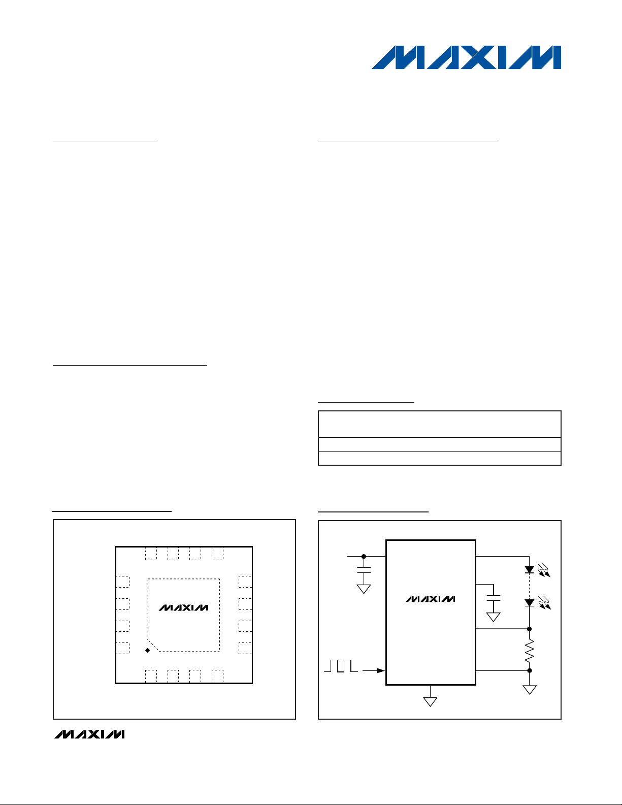
Pin Configuration
Ordering Information
MAX16800
IN
OUT
V5
LEDs
R
SENSE
0.1µF
+6.5V TO +40V
+5V REG
CS+
0.1µF
CS-
EN
PWM DIMMING
GND
Simplified Diagram
19-3803; Rev 0; 8/05
For pricing, delivery, and ordering information, please contact Maxim/Dallas Direct! at
1-888-629-4642, or visit Maxim’s website at www.maxim-ic.com.
+Denotes lead-free package.
*EP = Exposed paddle.
PART
TEMP RANGE
PIN-
PKG
CODE
MAX16800ATE
T1655-3
MAX16800ATE+
T1655-3
PACKAGE
-40°C to +125°C 16 TQFN-EP*
-40°C to +125°C 16 TQFN-EP*
Page 2
MAX16800
High-Voltage, 350mA, Adjustable Linear
High-Brightness LED (HB LED) Driver
2 _______________________________________________________________________________________
ABSOLUTE MAXIMUM RATINGS
ELECTRICAL CHARACTERISTICS
(VIN= +12V, EN = VIN, CV5= 0.1µF to GND, IV5= 0, CS- = GND, connect R
SENSE
= 0.58Ω between CS+ and CS-. Connect OUT to
CS+ (Note 1). T
J
= -40°C to +125°C, unless otherwise noted. Typical values are at TA= +25°C.) (Note 2)
Stresses beyond those listed under “Absolute Maximum Ratings” may cause permanent damage to the device. These are stress ratings only, and functional
operation of the device at these or any other conditions beyond those indicated in the operational sections of the specifications is not implied. Exposure to
absolute maximum rating conditions for extended periods may affect device reliability.
IN, OUT, and EN to GND........................................-0.3V to +45V
CS+, V5 to GND .......................................................-0.3V to +6V
CS- to GND............................................................-0.3V to +0.3V
OUT Short Circuited to GND Duration
(at V
IN
= +16V) ........................................................60 minutes
Maximum Current Into Any Pin (except V
IN
and OUT) .......±20mA
Continuous Power Dissipation (T
A
= +70°C)
16-Pin TQFN 5mm x 5mm
(derate 33.3mW/
°
C above +70°C)............................2666.7mW
Operating Junction Temperature Range...........-40°C to +125°C
Junction Temperature......................................................+150°C
Storage Temperature Range .............................-65°C to +150°C
Lead Temperature (soldering, 10s) .................................+300°C
PARAMETER
CONDITIONS
UNITS
Supply Voltage Range V
IN
(Note 1) 6.5
V
Ground Current I
G
I
LOAD
= 350mA 1.4 3 mA
Shutdown Supply Current I
SHDN
EN ≤ 0.6V 12 40 µA
Guaranteed Output Current I
OUT
R
SENSE
= 0.55Ω
mA
Output Current Accuracy 35mA < I
OUT
< 350mA
%
I
OUT
= 350mA (current pulsed),
12V < V
IN
< 40V
0.5 1.2 V
Dropout Voltage (Note 3) ∆VDO
I
OUT
= 350mA (current pulsed),
6.5V < V
IN
< 40V
0.5 1.5 V
Current rising 5.4
Output Current Slew Rate
Current falling 90
mA/µs
Short-Circuit Current V
OUT
= 0V, VIN = 12V
mA
LOGIC INPUT
EN Input Current I
EN
nA
EN Input Voltage High V
IH
2.8 V
EN Input Voltage Low V
IL
0.6 V
Turn–On Time t
ON
EN rising edge to 90% of OUT
µs
CURRENT SENSE (Note 4)
Regulated R
SENSE
Voltage V
RSNS
V
SENSE
= V
CS+
- V
CS-
mV
Input Current (CS+) V
CS+
= 220mV -14 µA
Input Current (CS-) V
CS+
= 220mV
µA
SYMBOL
MIN TYP MAX
40.0
350
±3.5
400 600 800
135 350
197 204 211
100
+84
Page 3
MAX16800
High-Voltage, 350mA, Adjustable Linear
High-Brightness LED (HB LED) Driver
_______________________________________________________________________________________ 3
Note 1: Resistors were added from OUT to CS+ to aid with the power dissipation during testing.
Note 2: All devices 100% production tested at T
A
= +25°C. Limits over the operating temperature range are guaranteed by design.
Note 3: Dropout is measured as follows:
Connect R
O
= 27Ω from OUT to CS+. Connect R
SENSE
= 0.58Ω from CS+ to CS-. Set VIN= +12V (record V
OUT
as V
OUT1
).
Reduce V
IN
until V
OUT
= 0.97 x V
OUT1
(record as V
IN2
and V
OUT2
). ∆VDO= V
IN2
- V
OUT2
.
Note 4: I
V5
= 0mA.
Note 5: Current regulation varies with V5 load (see the Typical Operating Characteristics).
Note 6: Thermal shutdown does not function if the output of the 5V reference is shorted to ground.
ELECTRICAL CHARACTERISTICS (continued)
(VIN= +12V, EN = VIN, CV5= 0.1µF to GND, IV5= 0, CS- = GND, connect R
SENSE
= 0.58Ω between CS+ and CS-. Connect OUT to
CS+ (Note 1). T
J
= -40°C to +125°C, unless otherwise noted. Typical values are at TA= +25°C.) (Note 2)
PARAMETER
SYMBOL
CONDITIONS
MIN
TYP
MAX
UNITS
THERMAL OVERLOAD
Thermal-Shutdown Temperature
°C
Thermal-Shutdown Hysteresis 23 °C
+5V REGULATOR
Output Voltage Regulation V5 5.0
5.5 V
Output Voltage Change ∆V5 0 < I
LOAD
< 4mA (Note 5) 15 60 Ω
V5 Short-Circuit Current V5 = 0V (Note 6) 30 mA
Typical Operating Characteristics
(VIN= VEN= +12V, TA= +25°C, unless otherwise noted.)
OUTPUT CURRENT
vs. TEMPERATURE
MAX16800 toc01
TEMPERATURE (°C)
OUTPUT CURRENT (mA)
1109565 80-10 5 20 35 50-25
50
100
150
200
250
300
350
400
450
0
-40 125
I
LOAD
= 350mA
I
LOAD
= 35mA
I
LOAD
= 200mA
I
LOAD
= 100mA
(V
CS+
- V
CS-
) vs. OUTPUT CURRENT
MAX16800 toc02
OUTPUT CURRENT (mA)
(V
CS+
- V
CS-
) (V)
320290230 26080 110 140 170 20050
0.201
0.202
0.203
0.204
0.205
0.206
0.207
0.208
0.209
0.210
0.200
20 350
VIN = 12V
OUTPUT CURRENT
vs. INPUT VOLTAGE
MAX16800 toc03
INPUT VOLTAGE (V)
OUTPUT CURRENT (mA)
35305 10 15 20 25
50
100
150
200
250
300
350
400
0
040
+155
5.27
Page 4

MAX16800
High-Voltage, 350mA, Adjustable Linear
High-Brightness LED (HB LED) Driver
4 _______________________________________________________________________________________
Typical Operating Characteristics (continued)
(VIN= VEN= +12V, TA= +25°C, unless otherwise noted.)
DROPOUT VOLTAGE
vs. TEMPERATURE
MAX16800 toc04
TEMPERATURE (°C)
DROPOUT VOLTAGE (V)
1109565 80-10 5 20 35 50-25
0.1
0.2
0.3
0.4
0.5
0.6
0.7
0.8
0.9
1.0
0
-40 125
I
LOAD
= 350mA
SHUTDOWN CURRENT
vs. TEMPERATURE
MAX16800 toc05
TEMPERATURE (°C)
SHUTDOWN CURRENT (µA)
1109580655035205-10-25
5
10
15
20
25
30
35
0
-40 125
VIN = 40V
VIN = 20V
VIN = 12V
VIN = 6.5V
+5V REGULATOR OUTPUT
vs. TEMPERATURE
MAX16800 toc06
TEMPERATURE (°C)
5V REGULATOR OUTPUT (V)
1109580655035205-10-25
5.1
5.2
5.3
5.4
5.5
5.0
-40 125
I
LOAD
= 1mA
NO LOAD
I
LOAD
= 5mA
(V
CS+
- V
CS-
) vs. I
V5
MAX16800 toc07
IV5 (mA)
(V
CS+
- V
CS-
) (V)
764 52 31
0.199
0.200
0.201
0.202
0.203
0.204
0.205
0.206
0.207
0.208
0.209
0.210
0.198
08
I
LOAD
= 410mA
+5V REGULATOR OUTPUT vs. V
IN
MAX16800 toc08
V
IN
(V)
5V REGULATOR OUTPUT (V)
353025201510
5.15
5.20
5.25
5.30
5.10
540
LOAD = 1mA
NO LOAD
LOAD = 5mA
200Hz DIMMED OPERATION
MAX16800 toc09
1ms/div
V
IN
5V/div
0V
I
LOAD
200mA/div
I
LOAD
= 350mA, VIN = VEN,
V
IN
PULSED AT 200Hz (50% DUTY CYCLE)
200Hz DIMMED OPERATION EXPANDED
MAX16800 toc10
20µs/div
V
IN
5V/div
0V
0
I
LOAD
100mA/div
I
LOAD
= 350mA,
V
IN
= VEN,
V
IN
PULSED AT 200Hz
(50% DUTY CYCLE)
200Hz DIMMED OPERATION EXPANDED
MAX16800 toc11
4µs/div
V
IN
5V/div
0V
0
I
LED
100mA/div
I
LOAD
= 350mA,
V
IN
= VEN,
V
IN
PULSED AT 200Hz
(50% DUTY CYCLE)
200Hz DIMMED OPERATION
MAX16800 toc12
1ms/div
EN
10V/div
0V
0
I
LED
100mA/div
I
LOAD
= 350mA, VIN = 12V,
EN PULSED AT 200Hz (50% DUTY CYCLE)
Page 5

MAX16800
High-Voltage, 350mA, Adjustable Linear
High-Brightness LED (HB LED) Driver
_______________________________________________________________________________________ 5
Pin Description
PIN NAME FUNCTION
1, 16 OUT Current-Regulated Output. Connect pin 1 to pin 16.
2, 3 IN Positive Input Supply. Bypass IN with a 0.1µF (min) capacitor to GND. Connect pin 2 to pin 3.
4–8, 13, 14 N.C. Not Internally Connected
9 CS+
Positive Input of the Internal Differential Amplifier. Connect the current-sense resistor between CS+
and CS- to program the output current level.
10 CS-
Negative Input of the Internal Differential Amplifier. Connect the current-sense resistor between
CS- and CS+ to program the output current level.
11 V5 +5V Regulated Output. Connect a 0.1µF capacitor from V5 to GND.
12 GND Ground
15 EN Enable Input. Drive EN high to enable the output.
—EP
Exposed Pad. Connect to the ground plane for effective power dissipation. Do not use as the only
ground connection.
Functional Diagram
MAX16800
ENABLE
EN
REFERENCE
GENERATOR
REGULATOR
IN
V5
DIFFERENTIAL
SENSE
AMPLIFIER
THERMAL
SHUTDOWN
I_
REQ
IN
OUT
CS+
CS-
Detailed Description
The MAX16800 is a high-current regulator capable of
providing up to a total of 350mA of current to one or
more strings of high-brightness LEDs. A wide operating
input voltage range of +6.5V to +40V makes the
MAX16800 ideal for automotive applications. A +5V
regulated output provides up to 4mA of current to
power external circuitry. In addition, the MAX16800 fea-
tures thermal and output short-circuit protection. The
wide operating voltage range helps protect the
MAX16800 against large transients such as those
found in load-dump situations up to 40V.
The MAX16800 uses a feedback loop to control the output current. The differential voltage across the sense
resistor is compared to a fixed reference voltage, and
the error is amplified to serve as the drive to the internal
Page 6

MAX16800
High-Voltage, 350mA, Adjustable Linear
High-Brightness LED (HB LED) Driver
6 _______________________________________________________________________________________
power series pass device (see the Functional
Diagram). The regulation point is factory set at (V
CS+
-
V
CS-
) = 204mV ±3.5%. The regulated current is user
defined by the value of R
SENSE
.
The MAX16800 is a current controller internally optimized for driving the impedance range expected from
one or more HB LEDs.
+5V Regulator
The MAX16800 includes a fixed +5V output regulator
that delivers up to 4mA of load current for low-power
applications throughout the +6.5V to +40V input voltage range. Connect a 0.1µF compensation capacitor
from V5 to ground. Shorting V5 to ground disables the
thermal shutdown.
Thermal Protection
The MAX16800 enters a thermal-shutdown mode in the
event of overheating. This typically occurs in overload or
output short-circuit conditions. When the junction temperature exceeds TJ= +155°C (typ), the internal thermal-protection circuitry turns off the series pass device.
The MAX16800 recovers from thermal-shutdown mode
once the junction temperature drops by 23°C (typ). The
part will therefore protect itself by thermally cycling in the
event of a short-circuit or overload condition.
Applications Information
Programming the LED Current
The MAX16800 uses a sense resistor across CS+ and
CS- to set the LED current. The differential sense ampli-
fier connected across R
SENSE
provides ground-loop
immunity and low-frequency noise rejection. The LED
current is given by the equation below:
I
LED
= V
SENSE
/ R
SENSE
Input Voltage Considerations
For proper operation, the minimum input voltage must
always be +1.2V (+1.5V for V
IN
<+12V) higher than the
worst-case sum of all the forward drops of all seriesconnected LEDs to the output of the MAX16800. The
minimum operating voltage of the device is +6.5V. The
device will operate below +6.5V; however, output current may not meet the full regulation specification (see
the Typical Operating Characteristics).
Low-Frequency PWM at the Output
The MAX16800 provides pulsed or chopped current
dimming. Generally, high-brightness LEDs are binned
to match at their full-rated current; however, LEDs from
the same bin exhibit poor matching at currents other
than full-rated current. To achieve uniformity, HB LED
manufacturers recommend PWM pulsing of the LED
current at their full-rated value. There are two methods
for producing a PWM output. One method is by pulsing
the enable input (EN) while having a constant voltage
at IN. The other method is to connect EN to IN and
pulse both EN and IN. Both methods generate a regulated-amplitude PWM current (variable duty cycle) that
can provide control over the LED brightness (see
Figures 1 and 2).
3
4
2
1
10
9
11
12
56
IN
8
16 15 13
IN
C1
V
IN
N.C.
GND
V5
CS-
C2
D1
R
SENSE
CS+
MAX16800
7
N.C. N.C. N.C.N.C.
OUT EN N.C.N.C.
14
OUT
V
EN
I
LED
Figure 1. Pulse Application with VINat a Constant Voltage
3
4
2
1
10
9
11
12
56IN8
16 15 13
IN
C1
V
IN
N.C.
GND
V5
CS-
C2
D1
R
SENSE
CS+
MAX16800
7
N.C. N.C. N.C.N.C.
OUT EN N.C.N.C.
14
OUT
I
LED
Figure 2. Pulse Application with EN Connected to V
IN
Page 7

MAX16800
High-Voltage, 350mA, Adjustable Linear
High-Brightness LED (HB LED) Driver
_______________________________________________________________________________________ 7
Chip Information
PROCESS: BiCMOS
3
4
2
1
10
9
11
12
56
IN
8
16 15 13
IN
C1
V
IN
N.C.
GND
V5
CS-
C2
D1
R
SENSE
CS+
MAX16800
7
N.C. N.C. N.C.N.C.
OUT EN N.C.N.C.
14
OUT
Typical Operating Circuit
Page 8

MAX16800
High-Voltage, 350mA, Adjustable Linear
High-Brightness LED (HB LED) Driver
8 _______________________________________________________________________________________
Package Information
(The package drawing(s) in this data sheet may not reflect the most current specifications. For the latest package outline information
go to www.maxim-ic.com/packages
.)
QFN THIN.EPS
D2
(ND-1) X e
e
D
C
PIN # 1
I.D.
(NE-1) X e
E/2
E
0.08 C
0.10 C
A
A1
A3
DETAIL A
E2/2
E2
0.10 M C A B
PIN # 1 I.D.
b
0.35x45°
D/2
D2/2
L
C
L
C
e e
L
CC
L
k
LL
DETAIL B
L
L1
e
XXXXX
MARKING
H
1
2
21-0140
PACKAGE OUTLINE,
16, 20, 28, 32, 40L THIN QFN, 5x5x0.8mm
-DRAWING NOT TO SCALE-
L
e/2
Page 9

MAX16800
High-Voltage, 350mA, Adjustable Linear
High-Brightness LED (HB LED) Driver
Maxim cannot assume responsibility for use of any circuitry other than circuitry entirely embodied in a Maxim product. No circuit patent licenses are
implied. Maxim reserves the right to change the circuitry and specifications without notice at any time.
Maxim Integrated Products, 120 San Gabriel Drive, Sunnyvale, CA 94086 408-737-7600 _____________________ 9
© 2005 Maxim Integrated Products Printed USA is a registered trademark of Maxim Integrated Products, Inc.
Quijano
Package Information (continued)
(The package drawing(s) in this data sheet may not reflect the most current specifications. For the latest package outline information
go to www.maxim-ic.com/packages
.)
COMMON DIMENSIONS
3.353.15T2855-1 3.25 3.353.15 3.25
MAX.
3.20
EXPOSED PAD VARIATIONS
3.00T2055-2 3.10
D2
NOM.MIN.
3.203.00 3.10
MIN.E2NOM. MAX.
NE
ND
PKG.
CODES
1. DIMENSIONING & TOLERANCING CONFORM TO ASME Y14.5M-1994.
2. ALL DIMENSIONS ARE IN MILLIMETERS. ANGLES ARE IN DEGREES.
3. N IS THE TOTAL NUMBER OF TERMINALS.
4. THE TERMINAL #1 IDENTIFIER AND TERMINAL NUMBERING CONVENTION SHALL
CONFORM TO JESD 95-1 SPP-012. DETAILS OF TERMINAL #1 IDENTIFIER ARE
OPTIONAL, BUT MUST BE LOCATED WITHIN THE ZONE INDICATED. THE TERMINAL #1
IDENTIFIER MAY BE EITHER A MOLD OR MARKED FEATURE.
5. DIMENSION b APPLIES TO METALLIZED TERMINAL AND IS MEASURED BETWEEN
0.25 mm AND 0.30 mm FROM TERMINAL TIP.
6. ND AND NE REFER TO THE NUMBER OF TERMINALS ON EACH D AND E SIDE RESPECTIVELY.
7. DEPOPULATION IS POSSIBLE IN A SYMMETRICAL FASHION.
8. COPLANARITY APPLIES TO THE EXPOSED HEAT SINK SLUG AS WELL AS THE TERMINALS.
9. DRAWING CONFORMS TO JEDEC MO220, EXCEPT EXPOSED PAD DIMENSION FOR T2855-1,
T2855-3, AND T2855-6.
NOTES:
SYMBOL
PKG.
N
L1
e
E
D
b
A3
A
A1
k
10. WARPAGE SHALL NOT EXCEED 0.10 mm.
JEDEC
T1655-1 3.203.00 3.10 3.00 3.10 3.20
0.70 0.800.75
4.90
4.90
0.25
0.250--
4
WHHB
4
16
0.350.30
5.10
5.105.00
0.80 BSC.
5.00
0.05
0.20 REF.
0.02
MIN. MAX.NOM.
16L 5x5
3.10
T3255-2
3.00
3.20
3.00 3.10 3.20
2.70
T2855-2 2.60 2.602.80 2.70 2.80
L
0.30 0.500.40
---
---
WHHC
20
5
5
5.00
5.00
0.30
0.55
0.65 BSC.
0.45
0.25
4.90
4.90
0.25
0.65
--
5.10
5.10
0.35
20L 5x5
0.20 REF.
0.75
0.02
NOM.
0
0.70
MIN.
0.05
0.80
MAX.
---
WHHD-1
28
7
7
5.00
5.00
0.25
0.55
0.50 BSC.
0.45
0.25
4.90
4.90
0.20
0.65
--
5.10
5.10
0.30
28L 5x5
0.20 REF.
0.75
0.02
NOM.
0
0.70
MIN.
0.05
0.80
MAX.
---
WHHD-2
32
8
8
5.00
5.00
0.40
0.50 BSC.
0.30
0.25
4.90
4.90
0.50
--
5.10
5.10
32L 5x5
0.20 REF.
0.75
0.02
NOM.
0
0.70
MIN.
0.05
0.80
MAX.
0.20 0.25 0.30
DOWN
BONDS
ALLOWED
NO
YES3.103.00 3.203.103.00 3.20T2055-3
3.103.00 3.203.103.00 3.20T2055-4
T2855-3 3.15 3.25 3.35 3.15 3.25 3.35
T2855-6 3.15 3.25 3.35 3.15 3.25 3.35
T2855-4 2.60 2.70 2.80 2.60 2.70 2.80
T2855-5 2.60 2.70 2.80 2.60 2.70 2.80
T2855-7 2.60 2.70
2.80
2.60 2.70 2.80
3.203.00 3.10T3255-3 3.203.00 3.10
3.203.00 3.10T3255-4 3.203.00 3.10
NO
NO
NO
NO
NO
NO
NO
NO
YES
YES
YES
YES
3.203.00T1655-2 3.10 3.00 3.10 3.20 YES
NO3.203.103.003.10T1655N-1 3.00 3.20
3.353.15T2055-5 3.25 3.15 3.25 3.35
YES
3.35
3.15T2855N-1 3.25 3.15 3.25 3.35
NO
3.35
3.15T2855-8 3.25 3.15 3.25 3.35
YES
3.203.10T3255N-1 3.00
NO
3.203.103.00
L
0.40
0.40
**
**
**
**
**
**
**
**
**
**
**
**
**
**
**
**
**
**
**
SEE COMMON DIMENSIONS TABLE
±0.15
11. MARKING IS FOR PACKAGE ORIENTATION REFERENCE ONLY.
H
2
2
21-0140
PACKAGE OUTLINE,
16, 20, 28, 32, 40L THIN QFN, 5x5x0.8mm
-DRAWING NOT TO SCALE-
12. NUMBER OF LEADS SHOWN ARE FOR REFERENCE ONLY.
3.30T4055-1 3.20 3.40 3.20 3.30 3.40
**
YES
0.0500.02
0.600.40 0.50
10
-----
0.30
40
10
0.40 0.50
5.10
4.90 5.00
0.25 0.35 0.45
0.40 BSC.
0.15
4.90
0.250.20
5.00 5.10
0.20 REF.
0.70
MIN.
0.75 0.80
NOM.
40L 5x5
MAX.
13. LEAD CENTERLINES TO BE AT TRUE POSITION AS DEFINED BY BASIC DIMENSION "e", ±0.05.
 Loading...