

Page 1
General Description
The MAX1677 is a compact, high-efficiency, dual-output boost converter for portable devices needing two
regulated supplies, typically for logic and liquid crystal
displays (LCDs). Operation with inputs as low as 0.7V
allows the MAX1677 to accept 1, 2, or 3-cell alkaline,
NiCd, or NiMH batteries as well as 1-cell lithium-ion batteries. The device requires no external FETs and can
maintain regulation while consuming only 20µA, making
it ideal for hand-held pen-input and PDA devices operating with low-current “sleep” states.
The MAX1677’s primary regulator supplies up to
350mA at either a factory-preset 3.3V or an adjustable
2.5V to 5.5V output. On-chip synchronous rectification
provides efficiencies up to 95%. 300kHz (or externally
clocked) pulse-width-modulation (PWM) operation is
particularly suitable for applications needing low noise,
such as those with wireless features. The primary converter also features pin-selectable pulse-frequencymodulation (PFM) operation that consumes only 20µA.
A 1µA shutdown state also minimizes battery drain.
The MAX1677’s secondary step-up converter supplies up
to +28V or -28V for LCD bias, varactor tuning, or other
high-voltage, low-current functions. Other MAX1677 features include precision reference, logic control inputs for
both regulators, and an uncommitted comparator for
low-battery detection or a reset function. The MAX1677
is supplied in Maxim’s compact 16-pin QSOP package,
which occupies no more space than a standard SO-8.
Applications
PDAs Portable Phones
Hand-Held Terminals Portable Instruments
Features
♦ No External FETs Required
♦ Main Output
Up to 350mA for Logic Supply
Fixed 3.3V or Adjustable (2.5V to 5.5V)
Synchronous Rectification for High Efficiency
(up to 95%)
300kHz (200kHz to 400kHz Synchronizable)
Fixed-Frequency PWM Operation
♦ Secondary Output
Up to +28V or -28V for LCD Bias
Programmable Current Limit
♦ 0.7V to 5.5V Input Voltage Range
♦ 20µA Quiescent Current
♦ 1µA Shutdown Current
♦ Low-Battery Comparator
♦ Small 16-Pin QSOP Package
MAX1677
Compact, High-Efficiency, Dual-Output
Step-Up and LCD Bias DC-DC Converter
________________________________________________________________ Maxim Integrated Products 1
19-1403; Rev 1; 3/01
PART
MAX1677EEE -40°C to +85°C
TEMP RANGE PIN-PACKAGE
16 QSOP
EVALUATION KIT
AVAILABLE
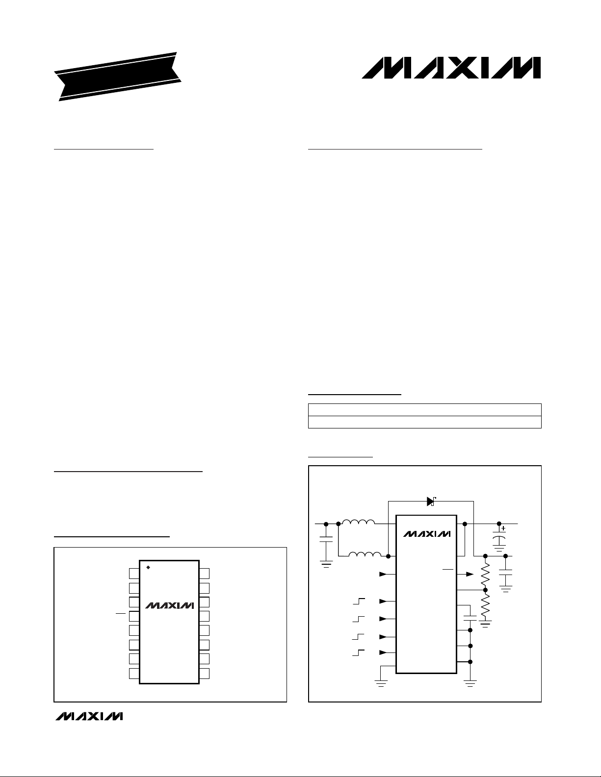
Pin Configuration
Ordering Information
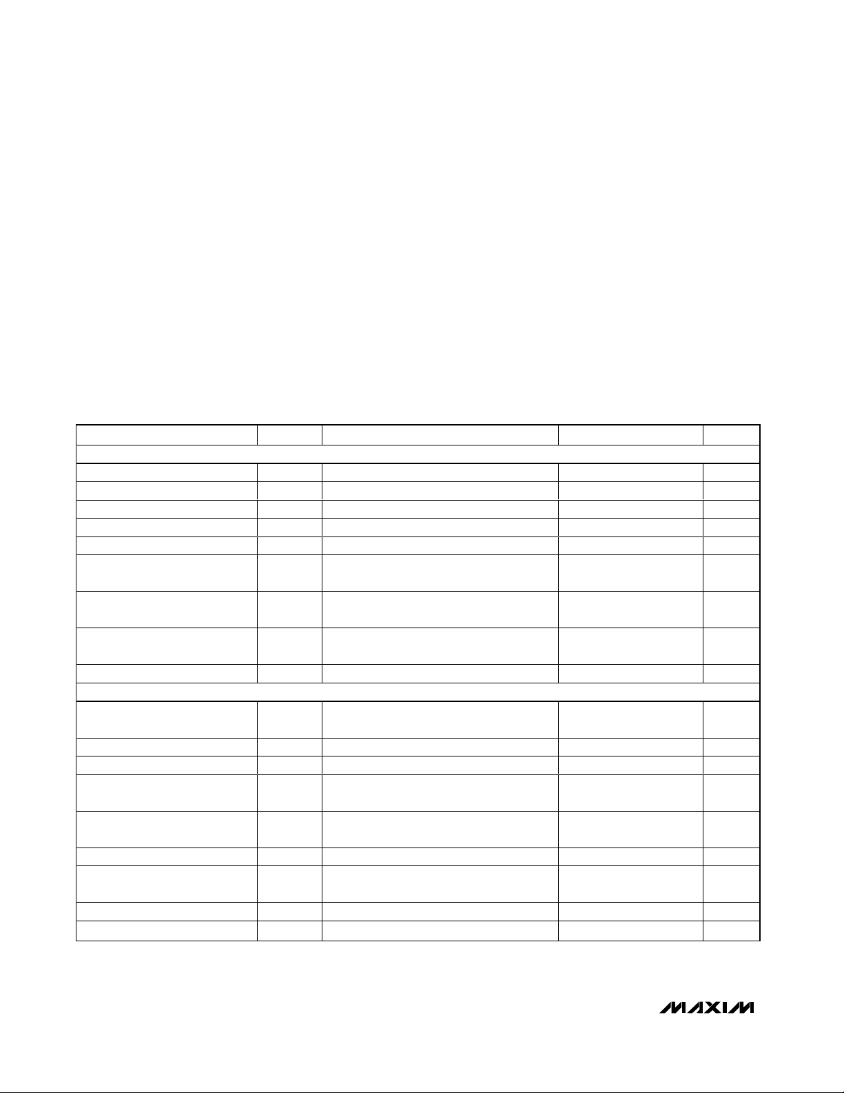
Typical Operating Circuit
MAX1677
LX
POUT
OUT
±28V
LCD
BOOST
OUTPUT
3.3V MAIN
BOOST OUTPUT
LCDFB
REF
FB
LCDGND
GND
LCDLX
LCDON
LBI
ON
OFF
LBO
CLK/SEL
ON
LCDPOL
PGND
PWM
PFM
ON
OFF
+VE OUT
-VE OUT
V
IN
= 0.7V to 5.5V
(UP TO MAIN
OUT
)
For pricing, delivery, and ordering information, please contact Maxim/Dallas Direct! at
1-888-629-4642, or visit Maxim’s website at www.maxim-ic.com.
TOP VIEW
1
OUT POUT
FB
2
LBI
3
4
LBO
CLK/SEL
5
LCDON
6
LCDPOL
7
REF
8
MAX1677
QSOP
16
15
14
13
12
11
10
9
LX
PGND
LCDGND
LCDLX
ON
LCDFB
GND
Page 2
MAX1677
Compact, High-Efficiency, Dual-Output
Step-Up and LCD Bias DC-DC Converter
2 _______________________________________________________________________________________
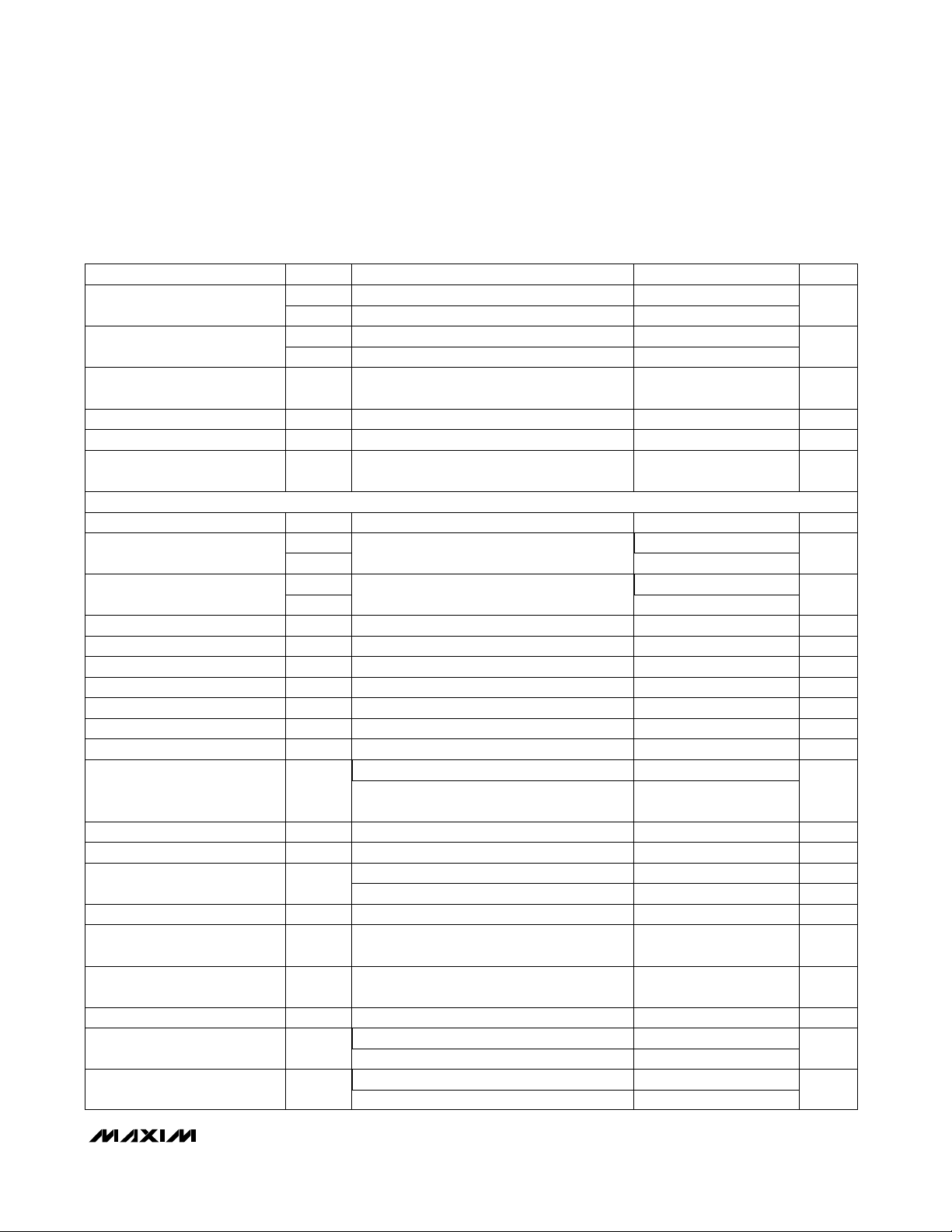
ABSOLUTE MAXIMUM RATINGS
ELECTRICAL CHARACTERISTICS
(V
OUT
= 3.3V, C
REF
= 0.1µF, POUT = OUT, TA= 0°C to +85°C, unless otherwise noted. Typical values are at TA= +25°C.)
Stresses beyond those listed under "Absolute Maximum Ratings" may cause permanent damage to the device. These are stress ratings only, and functional
operation of the device at these or any other conditions beyond those indicated in the operational sections of the specifications is not implied. Exposure to
absolute maximum rating conditions for extended periods may affect device reliability.
OUT, LCDON, ON, POUT, LBI, LBO,
LX to GND .............................................................-0.3V to +6V
CLK/SEL, LCDPOL, REF, LCDFB,
FB to GND .............................................-0.3V to (V
OUT
+ 0.3V)
LCDLX to GND .......................................................-0.3V to +30V
PGND, LCDGND to GND ......................................-0.3V to +0.3V
POUT to OUT.........................................................-0.3V to +0.3V
Continuous Power Dissipation (T
A
= +70°C)
16-Pin QSOP (derate 8.3mW/°C above +70°C)...........696mW
Operating Temperature Range ...........................-40°C to +85°C
Junction Temperature......................................................+150°C
Storage Temperature Range .............................-65°C to +160°C
Lead Temperature (soldering, 10s) .................................+300°C
PARAMETER
CONDITIONS
UNITS
GENERAL
Input Voltage Range V
IN
(Note 1) 0.7 5.5 V
Minimum Startup Voltage
TA = +25°C, I
LOAD
< 1mA 0.9 1.1 V
Reference Voltage V
REF
I
REF
= 0
V
Reference Load Regulation I
REF
= 0 to 50µA (Note 2) 2 15 mV
Reference Line Rejection V
OUT
= 2.5V to 5.5V 0.2 5 mV
Supply Current
Main DC On, LCD Off
No load, current into OUT 20 40 µA
Supply Current All On,
Main DC-DC in PFM Mode
I
PFM
No load, current into OUT 35 60 µA
Supply Current All On,
Main DC-DC in PWM Mode
I
PWM
No load, current into OUT
µA
Supply Current in Shutdown 0.3 5 µA
MAIN BOOST DC-DC
Output Voltage V
OUT
FB = GND, 0 ≤ ILX ≤ 350mA,
CLK/SEL = OUT (Note 3)
V
FB Regulation Voltage
)
V
FB Input Current I
FB
VFB = 1.3V
50 nA
Output Voltage Adjustment
Range
2.5 5.5 V
Startup to Normal Mode
Transition Voltage (Note 4)
2.1 2.4 V
Line Regulation I
OUT
= 150mA, VIN = 2V to 3V 0.6 %
Load Regulation
CLK/SEL = OUT, V
IN
= 2.4V,
I
LOAD
= 10mA to 200mA
1%
Frequency in Startup Mode
V
OUT
= 15V 40
kHz
LX Leakage Current
)
0.2 5 µA
SYMBOL
V
STARTUP
MIN TYP MAX
1.23 1.25 1.27
I
LCDOFF
V
FB (REG
V
LOCKOUT
f
STARTUP
I
LX (LEAK
3.20 3.30 3.43
Adjustable mode, CLK/SEL = OUT (Note 3) 1.225 1.25 1.275
115 300
0.02
300
Page 3
MAX1677
Compact, High-Efficiency, Dual-Output
Step-Up and LCD Bias DC-DC Converter
_______________________________________________________________________________________ 3
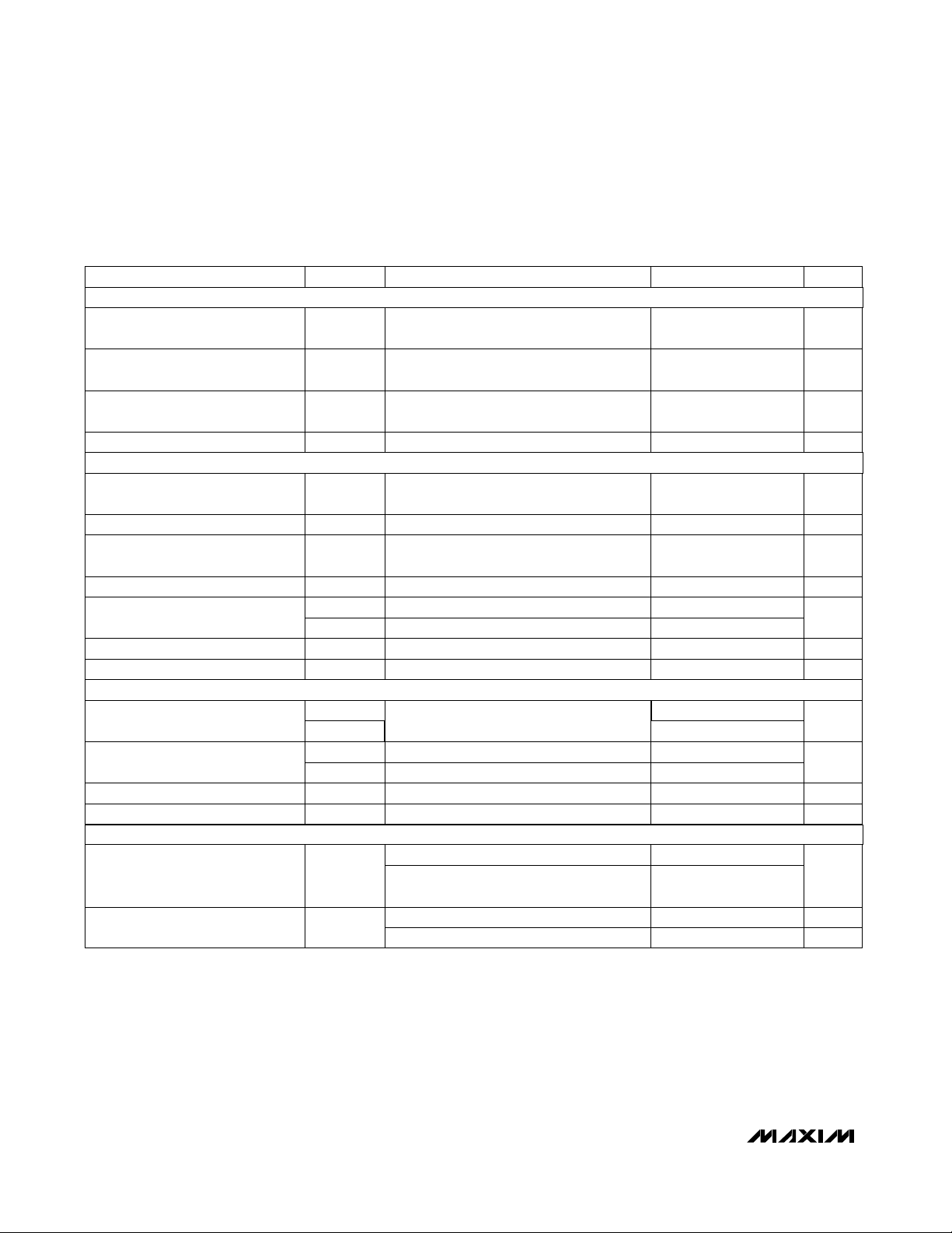
ELECTRICAL CHARACTERISTICS (continued)
(V
OUT
= 3.3V, C
REF
= 0.1µF, POUT = OUT, TA= 0°C to +85°C, unless otherwise noted. Typical values are at TA= +25°C.)
CONDITIONS
N-channel 0.22 0.5
Ω
P-channel 0.4 1.0
LX Current Limit
I
LX(PWM)
N-channel PWM mode 550 670 800
mA
UNITSMIN TYP MAXPARAMETER
I
LX(PFM)
N-channel PFM mode 250 350 450
P-Channel Synchronous Rectifier
Turn-Off Current in PFM Mode
40 90 140 mA
Internal Oscillator f CLK/SEL = OUT 240 300 360 kHz
Oscillator Maximum Duty Cycle D 80 85 90 %
External Clock Frequency
Range
200 400 kHz
ON Input Threshold
V
ON(LOW)
V
ON(HIGH)
LCDON, LCDPOL, CLK/SEL
Input Threshold
V
IL
V
OUT
> 2.5V
0.2V
OUT
V
V
IH
0.8V
OUT
LBI Falling Threshold V
LBI(TH)
599 614 629 mV
LBI Hysteresis 1 %
LBO Output Low Voltage
V
LBO(LO)
Sink current = 1mA 0.1 V
LBI Input Bias Current I
LBI(BIAS)
50 nA
LBO Leakage Current
I
LBO(LEAK)VLBO
= 5.5V 1 µA
LCDLX Voltage 28 V
LCDPOL connected to OUT or GND through
50kΩ
150 225 300
mA
LCDLX Switch Resistance RLCDLX V
OUT
= 3.3V 1.0 1.4 Ω
LCDLX Leakage Current V
LCDLX
= 28V 1 µA
LCDFB Set Point
Positive LCD, LCDPOL = OUT 1.225 1.25 1.275 V
Negative LCD, LCDPOL = GND -15 0 15 mV
LCDFB Input Bias Current 50 nA
LCD Line Regulation
I
LOAD
= 5mA, VIN= 1.2V to 3.6V,
Figure 2
0.1 %/V
LCD Load Regulation
I
LOAD
= 0 to 5mA, VIN= 2.4V,
Figure 2
0.5 %
Maximum LCDLX On-Time t
ON LCD
3.4 4.3 5.2 µs
1.1V < V
OUT
< 5.5V
0.8V
OUT
0.2V
OUT
V
LX On-Resistance
SYMBOL
R
LX(ON)N
R
LX(ON)P
LCDPOL = OUT or GND 300 350 450
LCDLX Switch Current Limit
Input Leakage Current ON, LCDON, LCDPOL, CLK/SEL 1 µA
Minimum LCDLX Off-Time
Operating mode 0.8 1 1.2
µs
Start-up mode (positive or negative) 3.0 4.0 5.0
LCDFB Voltage for
Startup Mode
LCDPOL = OUT 0.75
V
LCDPOL = GND 0.5
LOGIC AND CONTROL INPUTS
Page 4
MAX1677
Compact, High-Efficiency, Dual-Output
Step-Up and LCD Bias DC-DC Converter
4 _______________________________________________________________________________________
Note 1: The MAX1677 operates in bootstrap mode (operates from the output voltage). Once started, it will operate down to 0.7V
input. If V
IN
exceeds the set V
OUT
, V
OUT
will follow one diode drop below VIN.
Note 2: C
REF
= 0.22µF for applications where I
REF
> 10µA.
Note 3: In low-power mode (CLK/SEL = GND), the output voltage regulates 1% higher than in low-noise mode (CLK/SEL = OUT or
synchronized).
Note 4: The device is in a startup mode when V
OUT
is below this value.
Note 5: Specifications to -40°C are guaranteed by design and not production tested.
ELECTRICAL CHARACTERISTICS
(V
OUT
= 3.3V, C
REF
= 0.1µF, POUT = OUT, TA= -40°C to +85°C, unless otherwise noted. ) (Note 5)
LBO Output Low Voltage
V
LBO(LO)
Sink current = 1mA
LCDPOL = OUT or GND 300 450
0.1 V
µA
Supply Current
Main DC On, LCD Off
Supply Current All On,
Main DC-DC in PFM Mode
I
PFM
No load, current into OUT 60 µA
VFB Regulation Voltage
µALX Leakage Current
Startup to Normal Mode Transition
Voltage (Note 4)
CONDITIONS
V
LOCKOUT
2.1 2.4 V
I
LX(LEAK)
5
Output Voltage V
OUT
FB = GND, 0 ≤ ILX≤ 350mA,
CLK/SEL = OUT (Note 3)
3.17 3.46 V
V
FB(REG)
Adjustable mode, CLK/SEL = OUT (Note 3) 1.22 1.28
µA
Supply Current All On,
Main DC-DC in PWM Mode
Supply Current in Shutdown 5 µA
I
PWM
No load, current into OUT 300
I
LCDOFF
No load, current into OUT 40
LX Current Limit
I
LX(PWM)
N-channel PWM mode 550 900
mA
UNITSMIN MAXSYMBOLPARAMETER
I
LX(PFM)
N-channel PFM mode 250 500
Internal Oscillator f CLK/SEL = OUT 240 360 kHz
External Clock Frequency Range 200 400 kHz
ON Input Threshold
V
ON(LOW)
1.1V < V
OUT
< 5.5V
0.2V
OUT
V
V
ON(HIGH)
0.8V
OUT
LCDON, LCDPOL, CLK/SEL
Input Threshold
V
IL
0.2V
OUT
V
V
IH
0.8V
OUT
LBI Falling Threshold V
LBI(TH)
599 629 mV
LCD BIAS DC-DC
LCDLX Switch Current Limit
LCDPOL connected to OUT or GND
through 50kΩ
150 300
mA
LCDFB Set Point
Positive LCD, LCDPOL = OUT 1.22 1.28 V
-20 +20Negative LCD, LCDPOL = GND mV
GENERAL
MAIN
LCD BIAS DC-DC
LOGIC
Page 5
MAX1677
Compact, High-Efficiency, Dual-Output
Step-Up and LCD Bias DC-DC Converter
_______________________________________________________________________________________ 5
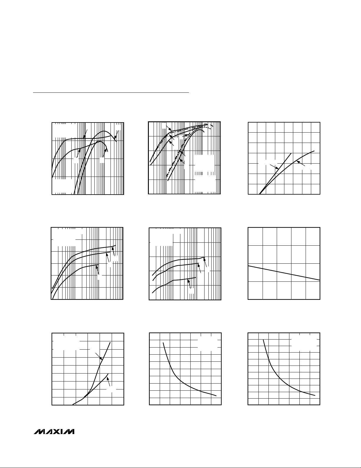
0.1 101 100 1000
EFFICIENCY vs. LOAD CURRENT
(V
OUT
= 3.3V)
MAX1677-01
LOAD CURRENT (mA)
EFFICIENCY (%)
100
60
70
80
90
PWM MODE
C = 2.4V
D = 1.2V
PFM MODE
A = VIN = 2.4V
B = VIN = 1.2V
C
D
B
A
100
80
60
40
20
0
0.1 1 10 100 1000
EFFICIENCY vs. LOAD CURRENT
(V
OUT
= 5V)
MAX1677-02
LOAD CURRENT (mA)
EFFICIENCY (%)
PWM MODE
A: V
IN
= 3.6V
B: VIN = 2.4V
C: VIN = 1.2V
A
D
E
F
B
C
PFM MODE
D: VIN = 3.6V
E: VIN = 2.4V
F: VIN = 1.2V
0
100
300
200
500
600
400
700
01.01.50.5 2.0 2.5 3.0 3.5 4.0
MAXIMUM LOAD CURRENT
vs. BATTERY INPUT VOLTAGE
(PWM MODE)
MAX1677-03
INPUT VOLTAGE (V)
LOAD CURENT (mA)
V
OUT
= 3.3V
V
OUT
= 5V
40
0.1 100101
EFFICIENCY vs. LOAD CURRENT
(LCD V
OUT
= 12V)
100
60
50
80
90
70
MAX1677-04
LOAD CURRENT (mA)
EFFICIENCY (%)
CIRCUIT OF FIGURE 2
A: VIN = 3.6V
B: VIN = 2.4V
C: VIN = 1.2V
A
B
C
50
0.1 100101
EFFICIENCY vs. LOAD CURRENT
(LCD V
OUT
= 20V)
100
70
60
90
80
MAX1677-05
LOAD CURRENT (mA)
EFFICIENCY (%)
CIRCUIT OF FIGURE 2
A: VIN = 3.6V
B: V
IN
= 2.4V
C: V
IN
= 1.2V
A
B
C
1.2450
1.2475
1.2525
1.2500
1.2550
0 20406080100
REFERENCE VOLTAGE
vs. REFERENCE CURRENT
MAX1677-06
REFERENCE CURRENT (µA)
REFERENCE VOLTAGE (V)
Typical Operating Characteristics
(Circuits of Figures 2 and 3, TA = +25°C, unless otherwise noted.)
0
100
50
250
200
150
400
350
300
450
01.00.5 1.5 2.0 2.5 3.0
LOAD CURRENT
vs. STARTUP VOLTAGE
MAX1677-07
START-UP VOLTAGE (V)
LOAD CURRENT (mA)
PWM
PFM
V
OUT
= 3.3V
TESTED WITH
RESISTIVE LOAD
0
0.06
0.04
0.02
0.10
0.08
0.18
0.16
0.14
0.12
0.20
0 0.5 1.0 1.5 2.0 2.5 3.0 3.5
NO-LOAD SUPPLY CURRENT vs.
INPUT VOLTAGE (LCD OFF)
MAX1677-08
INPUT VOTAGE (V)
SUPPLY CURRENT (mA)
V
OUT
= 3.3V
PFM MODE
LCD OFF
0
0.1
0.2
0.3
0.4
0.5
0.6
0.7
0.8
0.9
1.0
1.1
0 0.5 1.0 1.5 2.0 2.5 3.0 3.5
NO-LOAD SUPPLY CURRENT vs.
INPUT VOLTAGE (LCD ON)
MAX1677-09
INPUT VOLTAGE (V)
SUPPLY CURRENT (mA)
V
OUT
= 3.3V
PFM MODE
V
LCD
= -20V
Page 6

MAX1677
Compact, High-Efficiency, Dual-Output
Step-Up and LCD Bias DC-DC Converter
6 _______________________________________________________________________________________
10mV/
div
V
LX
I
LX
V
RIPPLE
200mA/
div
100mV/
div
5µs/div
LCD SWITCHING WAVEFORMS
MAX1677-13
LDCLX CURRENT LIMIT = 350mA,
2.4V
IN,
+12V
OUT,
10mA LOAD
10mV/
div
V
LX
I
LX
V
RIPPLE
200mA/
div
100mV/
div
2µs/div
LCD SWITCHING WAVEFORMS
(50kΩ FROM LCDPOL TO OUT)
MAX1677-14
LCDLX CURRENT LIMIT = 225mA,
2.4V
IN,
+12V
OUT,
10mA LOAD
50mV/
div
I
OUT
V
RIPPLE
200mA/
div
2ms/div
MAIN BOOST CONVERTER
LOAD TRANSIENT
MAX1677-15
V
IN
= 2.4V, V
OUT
= 3.3V
I
LOAD
= 0 to 200mA
2V/
div
V
LX
I
LX
V
RIPPLE
100mA/
div
50mV/
div
1µs/div
MAIN BOOST CONVERTER SWITCHING
WAVEFORMS (PWM MODE)
MAX1677-10
2.4VIN, 3.3V
OUT
,
200mA I
OUT
2V/
div
V
LX
I
LX
V
RIPPLE
100mA/
div
20mV/
div
2µs/div
MAIN BOOST CONVERTER SWITCHING
WAVEFORMS (PFM MODE)
MAX1677-11
1.2VIN, 3.3V
OUT
,
20mA I
OUT
2V/
div
V
LX
I
LX
V
RIPPLE
100mA/
div
50mV/
div
10µs/div
MAIN BOOST CONVERTER SWITCHING
WAVEFORMS (PFM MODE, 50mA OUTPUT)
MAX1677-12
PFM, 1.2V
IN
,
3.3V
OUT
, 50mA I
OUT
Typical Operating Characteristics (continued)
(Circuits of Figures 2 and 3, TA= +25°C, unless otherwise noted.)
Page 7

MAX1677
Compact, High-Efficiency, Dual-Output
Step-Up and LCD Bias DC-DC Converter
_______________________________________________________________________________________ 7
1V/
div
0V
V
OUT
V
IN
50mV/
div
5ms/div
MAIN BOOST CONVERTER
LINE TRANSIENT
MAX1677-16
V
IN
= 2V TO 3V, V
OUT
= 3.3V,
I
LOAD
= 150mA
1V/
div
0V
V
LCD
V
IN
50mV/
div
5ms/div
LCD LINE TRANSIENT
(V
LCD
= +12V)
MAX1677-17
V
IN
= 2V TO 3V, V
LCD
= +12V,
I
OUT
= 5mA
1V/
div
V
OUT
ON
1V/
div
0V
500µs/div
MAIN BOOST CONVERTER
STARTUP DELAY
MAX1677-19
V
IN
= 2.4V, V
OUT
= 3.3V,
I
LOAD
= 10mA
Typical Operating Characteristics (continued)
(Circuits of Figures 2 and 3, TA= +25°C, unless otherwise noted.)
2V/
div
V
LCD
LCDON
10V/
div
10ms/div
LCD STARTUP DELAY
MAX1677-20
V
IN
= 2.4V, V
LCD
= -20V,
I
OUT
= 5mA
1V/
div
0V
V
LCD
V
IN
50mV/
div
5ms/div
LCD LINE TRANSIENT
(V
LCD
= -20V)
MAX1677-18
V
IN
= 2V TO 3V, V
LCD
= -20V,
I
OUT
= 5mA
Page 8

MAX1677
Compact, High-Efficiency, Dual-Output
Step-Up and LCD Bias DC-DC Converter
8 _______________________________________________________________________________________
Pin Description
Dual Mode is a trademark of Maxim Integrated Products.
Detailed Description
The MAX1677 is a highly-efficient, dual-output power
supply for battery-powered devices. On-chip are two
complete step-up DC-DC converters to power main
logic and bias an LCD (Figure 1). The main boost converter (MBC) has on-chip P-channel and N-channel
MOSFETs that provide synchronous-rectified voltage
conversion for maximum efficiency at loads up to
300mA. See Table 1 for available output current with
typical battery configurations. The output voltage of the
MBC is factory-preset to 3.3V, or can be set from 2.5V
to 5.5V with external resistors (dual-mode operation).
Either fixed-frequency PWM or low-operating-current
PFM operation can be selected for the MBC using the
CLK/SEL input (Table 2).
The LCD boost converter (LCD) includes an internal Nchannel DMOS switch to generate positive or negative
voltages up to ±28V. The polarity of the LCD output is
set by LCDPOL input (Table 3). Figure 2 shows the
MAX1677 configured for a positive LCD output voltage
with a 3.3V main output. Figure 3 shows the MAX1677
configured for a negative LCD output. LCDPOL also
allows the current limit of LCDLX to be reduced from
350mA to 225mA to allow minimum-size inductors in
low-current LCD applications (typically for LCD loads
<10mA).
Also included in the MAX1677 are a precision 1.25V
reference that sources up to 50µA, logic shutdown control for the MBC and LCD (the MBC must be on for the
LCD to operate), and a low-battery comparator.
NAME FUNCTION
1 OUT
Output Sense Input. The device is powered from OUT. Bypass to GND with a 0.1µF ceramic capacitor.
Connect OUT to POUT through a 10Ω series resistor.
2 FB
Dual Mode™ Main Boost Feedback Input. Connect to GND for 3.3V output. Connect a voltage-divider from
OUT to FB to adjust the output in the 2.5V to 5.5V range (Figure 5).
PIN
3 LBI
Low-Battery-Comparator Input. Threshold is 614mV. Set the low-battery trip-point with an external voltage
divider (Figure 7).
4
LBO Open-Drain, Low-Battery Output. LBO is low when LBI is below 614mV, otherwise it remains high.
Sync Clock and PWM Select Input.
CLK/SEL = low: low-power, low-quiescent-current PFM mode.
CLK/SEL = high: low-noise, high-power PWM mode at 300kHz.
CLK/SEL = driven with external clock of 200kHz to 400kHz, synchronized PWM high-power mode.
5 CLK/SEL
10 LCDFB
LCD Feedback Input. Threshold is 1.25V for positive with LCDPOL high, and 0 for negative with
LCDPOL low.
9 GND Ground
8 REF 1.25V Reference Output. Bypass with 0.1µF.
7 LCDPOL LCD Polarity Select Input. Sets LCD boost converter polarity and peak current output (Table 2).
6 LCDON LCD Enable Input. Drive high to turn on LCD boost converter. Main DC-DC must also be on.
11 ON I.C. Enable Input. Drive high to enable the MAX1677.
12 LCDLX LCD Boost 28V Switch Drain
13 LCDGND Source of the Internal N-Channel DMOS LCD Boost-Converter Switch
14 PGND Source of the Internal N-Channel Main Boost-Converter Switch
15 LX Main Output Boost Internal Switch Drain
16 POUT
Boost DC-DC Converter Power Output. Source of internal P-channel MOSFET main boost-converter
synchronous rectifier.
Page 9

MAX1677
Compact, High-Efficiency, Dual-Output
Step-Up and LCD Bias DC-DC Converter
_______________________________________________________________________________________ 9
Main Boost Converter (MBC)
The MBC operates either in PFM mode, 300kHz PWM
mode, or externally synchronized PWM mode as selected by the CLK/SEL input (Table 2). PWM mode offers
fixed-frequency operation and maximum output power.
PFM mode offers the lowest IC operating current. LX
current limit is reduced in PFM mode to increase efficiency and minimize output ripple.
PWM Mode
When CLK/SEL is high, the MAX1677 operates in its
high-power, low-noise PWM mode, switching at the
300kHz internal oscillator frequency. The MOSFET
switch pulse-width is modulated to control the power
transferred on each switching cycle and regulate the
Table 1. Main Boost Converter Available
Output Current
Figure 1. Functional Block Diagram
NUMBER OF
CELLS
1 Alk/NiCd/NiMH 140/150
MBC OUTPUT
CURRENT
(mA)
PWM/PFM
1 Alk/NiCd/NiMH 1.2
1.2
INPUT
VOLTAGE
(V)
MBC
OUTPUT
VOLTAGE
(V)
3.3
5 100/70
2 Alk/NiCd/NiMH 2.4 3.3 350/170
2 Alk/NiCd/NiMH 2.4 5 260/125
1 Alk/NiCd/NiMH
or 1 Li-Ion
3.6 5 350/170
REF
LCDPOL
LCDFB
GND
ON
MAX1677
ON
REF
REFERENCE
ISET/POL SENSE
POL
IN
I
LCDLX
STARTUP OSC
OUT
ON
2.25V
501k
START-UP
839k
ST
EA
90% REF
I
LCDLX
CL
LCD ON
POL
LCD BIAS
ON
LCDDRV
MAIN DC-DC
SUCLK
EA
CLK
ON
50% REF
OUT
CLK/SEL
POUT
QP
LX
QN
PGND
FB
LBO
LBI
LCDON
LCDLX
LCDGND
Page 10

MAX1677
Compact, High-Efficiency, Dual-Output
Step-Up and LCD Bias DC-DC Converter
10 ______________________________________________________________________________________
output voltage. In PWM mode, the MBC can supply up
to 350mA. Switching harmonics generated by the fixedfrequency operation are consistent and easily filtered.
During PWM operation, the rising edge of the internal
clock sets a flip-flop, which turns on the N-channel
MOSFET (Figure 4). The switch turns off when the sum
of the voltage-error, slope-compensation, and currentfeedback signals trips the multi-input comparator and
resets the flip-flop; the switch remains off for the rest of
the cycle. Changes in the output voltage error signal
shift the inductor current level and modulate the MOSFET pulse width.
Clock-Synchronized PWM
The MAX1677 operates as a clock-synchronized current-mode PWM when a clock signal (200kHz to
400kHz) is applied to CLK/SEL. This allows switching
harmonics to be positioned to avoid sensitive frequency bands, such as those near IF frequencies in wireless
applications.
Low Power PFM Mode
Pulling CLK/SEL low places the MAX1677 in low-power
standby mode. During standby mode, PFM operation
regulates the output voltage by transferring a fixed
amount of energy during each cycle, and then modulating the switching frequency to control the power delivered to the output. The device switches only as needed
to service the load, resulting in the highest possible efficiency at light loads and an operating current of only
20µA. The MBC can supply up to 170mA when in PFM
mode (Table 1).
Figure 2. LCD Converter in Positive Mode
Figure 3. LCD Converter in Negative Mode
Figure 4. Controller Block Diagram in PWM Mode
R3
10Ω
POUT
MAX1677
LX
0.1µF
OUT
C4
GND
LCDLX
LCDON
CLK/SEL
ON
LCDPOL
PGND
OUT
0.1µF
C4
MAX1677
GND
LCDON
CLK/SEL
ON
LCDPOL
PGND
R3
10Ω
REF
FB
LCDGND
LCDFB
POUT
LX
LCDLX
REF
FB
LCDGND
LCDFB
L1
10µH
L2
10µH
C5
0.1µF
L1
10µH
L2
10µH
C5
0.1µF
R1
R2
R2
C6
0.1µF
3.3V MAIN
BOOST OUTPUT
3.3V MAIN
BOOST OUTPUT
MBR0530
R1
D2
MBR0530
C2
100µF
D3
C2
100µF
V
IN
C1
100µF
LCD BOOST OUTPUT
C3
4.7µF
D2
MBR0530
-LCD BOOST
OUTPUT
C3
4.7µF
C1
100µF
POUT
P
FEEDBACK
REF
PWM-MODE
CURRENT-
LIMIT LEVEL
OSC
RSQ
LX
N
PGND
V
IN
Page 11

MAX1677
Compact, High-Efficiency, Dual-Output
Step-Up and LCD Bias DC-DC Converter
______________________________________________________________________________________ 11
During PFM operation, the error comparator detects
when the output voltage is out of regulation and sets a
flip-flop, turning on the N-channel MOSFET switch
(Figure 5). When the inductor current ramps to the PFM
mode current limit (350mA), the current-sense comparator resets a flip-flop. The flip-flop turns off the N-channel
switch and turns on the P-channel synchronous rectifier.
The energy stored in the inductor is transferred to the
output through the P-channel switch. A second flip-flop,
previously reset by the switch’s “on” signal, inhibits the
next cycle until the inductor current is depleted and the
output is out of regulation. This forces operation with
discontinuous inductor current in PFM mode.
Startup Oscillator
The MBC employs a low-voltage startup oscillator to
ensure a 1.1V (0.9V typical) startup voltage. On startup, if the output voltage is less than 2.25V, the P-channel switch stays off and the N-channel pulses at a 25%
duty cycle. When the output voltage exceeds 2.25V,
the normal PWM or PFM control circuitry takes over.
Once the MBC is in regulation, it can operate with
inputs down to 0.7V since the internal power for the IC
is taken from OUT. The MBC cannot supply full output
current until OUT reaches 2.5V.
Synchronous Rectifier
The MAX1677 MBC features an internal 1Ω P-channel
synchronous rectifier. Synchronous rectification typically improves efficiency by 5% or more over similar nonsynchronous step-up designs. In PWM mode, the
synchronous rectifier turns on during the second half of
each cycle. In PFM mode, an internal comparator turns
on the synchronous rectifier when the voltage at LX
exceeds the MBC output, and then turns it off when the
inductor current drops below 90mA (typ).
The on-chip synchronous rectifier allows the external
Schottky diode to be omitted in designs that operate
from inputs exceeding 1.4V. In circuits operating below
1.4V (1-cell inputs, for example), connecting a Schottky
diode in parallel with the internal synchronous rectifier
(from LX to POUT) provides the lowest startup voltage.
LCD Boost Converter (LCD)
The LCD converter can be configured for a positive or
negative output by setting the LCDPOL pin and using
the appropriate circuit (Figures 2 and 3, and Table 3).
A combination of peak current limiting and a pair of
one-shot timers control LCD switching. During the oncycle the internal N-channel DMOS switch turns on,
and inductor current ramps up until either the switch
peak current limit is reached or the 5.2µs maximum ontime expires (typically at low input voltages). After the
on-cycle terminates, the switch turns off and the output
capacitor charges. The switch remains off until the error
comparator initiates another cycle.
The LCDLX current limit is set by LCDPOL, as outlined
in Table 3. The lower, 225mA peak current setting
allows tiny low-current “chip” inductors to be used
when powering smaller (less than 15 square inches)
liquid crystal panels. Use the following equation to
determine which LCDLX current-limit setting is
required.
I
LCD
= (0.7 × I
PK(LCD)
× V
IN(MIN)
) / (2 × V
LCD(MAX)
)
where I
LCD
is the output current, V
IN(MIN)
is the mini-
mum expected input voltage, V
LCD(MAX)
is the maxi-
mum required LCD output voltage, and I
PK(LCD)
is
350mA or 225mA as set by LCDPOL. The 0.7 term is a
correction factor to conservatively account for typical
switch, inductor, and diode losses.
The LCD boost is enabled when both ON and LCDON
are high, and the MBC output voltage is within 90% of
its set value. A soft-start startup mode with increased
CLK/SEL
0
1 PWM
Low-Power PFM
MBC MODE FEATURES
Lowest Supply Current
High Output Current,
Fixed-Frequency Ripple
Ext Clock
(200Hz to
400kHz)
Synchronized
PWM
High Output Current,
Synchronized Ripple
Frequency
Table 2. Selecting MBC Operating Mode
Figure 5. Controller Block Diagram in PFM Mode
Q
D
LOGIC HIGH
Q
R
POUT
P
V
FB
V
REF
CURRENT
LIMIT LEVEL
Q
S
R
N
PGND
LX
Page 12

off time reduces transient input current when the LCD is
activated.
Shutdown: ON and LCDON
A logic-low level at ON shuts down all MAX1677 circuits including the LCD converter, reference, and LBI
comparator. A logic-high level at LCDON activates the
LCD boost converter. The LCD boost converter can
only be activated when ON is high. When ON is low,
the MAX1677 draws 1µA.
Low-Battery Comparator
The MAX1677 has an on-chip comparator for low-battery detection. If the voltage at LBI falls below 614mV,
LBO (an open-drain output) sinks current to GND. The
low-battery trip level is set by two resistors (Figure 6).
Since the LBI input current is less than 50nA, large
resistor values (R6 ≤ 130kΩ) can be used to minimize
input loading. Calculate R5 as follows:
R5 = R6 [(V
TRIP
/ 0.614V) - 1]
Connect a pullup resistor (R8) to LBO when driving
CMOS logic. LBO is an open-drain output and can be
pulled as high as 6V regardless of the voltage at OUT.
When LBI is above 0.614V, LBO is high impedance. If
the LBI comparator is not used, ground LBI.
Since the low-battery comparator is noninverting, hysteresis can be added by connecting a resistor (R7)
from LBI to LBO as shown in Figure 7. When LBO is
high, the series combination of R8 and R7 source current into the summing node at LBI (no current flows into
the IC).
Design Procedure
The MBC feedback pin (FB) features Dual Mode operation. With FB grounded, the MBC output is preset to
3.3V. It can also be adjusted from 2.5V to 5.5V with
external resistors, R3 and R4, as shown in Figure 8. To
set the output voltage externally, select resistor R4 in
the 10kΩ to 200kΩ range. Calculate R3 using:
R3 = R4 [(V
OUT
/ 1.25V) - 1]
Setting the LCD Output Voltage
For either positive or negative LCD output voltages, set
the voltage with two external resistors, R1 and R2, as
shown in Figures 2 and 3. Since the input current at FB
has a maximum of 50nA, large resistors can be used
without significant accuracy loss. Begin by selecting R2
Figure 6. Setting the Low-Battery Trip Threshold
Figure 7. Adding External Hysteresis to the LBI Comparator
Figure 8. Setting the MBC Output Voltage Externally
MAX1677
Compact, High-Efficiency, Dual-Output
Step-Up and LCD Bias DC-DC Converter
12 ______________________________________________________________________________________
Table 3. Setting LCD Output Polarity and
Peak Inductor Current
225GND through 50kΩNegative
225OUT through 50kΩPositive
350
350
L
CDLX
PEAK
INDUCTOR CURRENT
(mA)
LCDPOL
CONNECTED TO:
OUT
GNDNegative
Positive
LCD
OUTPUT
POLARITY
(V
)
V
IN
TRIP
POUT
R5
MAX1677
LBI
R6
LBO
R8
LOGIC POWER
LOW-BATTERY OUTPUT
: VH, VL)
V
(V
IN
TRIP
R5
R6
R5 + R5
V
= 0.614V
H
R7 R6
WHERE VH IS THE RISING V
AND V
+
1
[
IS THE FALLING V
L
LBI
]
MAX1677
MAX1677
R7
LEVEL
TRIP
LEVEL.
TRIP
POUT
GND
POUT
LBO
VL = 0.614V + R5
FB
R8
100k
0.614V
V
POUT
-
( )
(
R6
R3
R4
R7 + R8
MBC OUTPUT
- 0.614V
)
Page 13

MAX1677
Compact, High-Efficiency, Dual-Output
Step-Up and LCD Bias DC-DC Converter
______________________________________________________________________________________ 13
in the 10kΩ to 200kΩ range and calculate R1 using one
of the following two equations (for positive or negative
output).
For a positive LCD output, connect LCDPOL to OUT as
shown in Figure 2. This sets the threshold at LCDFB to
1.25V. Select R2 and the desired output voltage
(V
LCD
), and calculate R1:
For positive LCD output: R1 = R2 [(V
LCD
/ 1.25V) - 1]
Figure 3 shows the standard circuit for generating a
negative LCD supply. This connection limits V
LCD
to
values between -VINand -28V. If a smaller negative
output voltage is required, D2’s cathode can be connected to VINrather than ground. This alternate connection permits output voltages from 0 to -28 - V
IN
.
For a negative LCD output voltage, connect LCDPOL to
GND. The feedback threshold voltage of LCDFB is set
to 0. Select R2 and the desired output voltage (V
LCD
),
and calculate R1:
For negative LCD output: R1 = R2 ×V
LCD
/ 1.25V
To minimize ripple in the LCD output and prevent subharmonic noise caused by switching pulse grouping, it
may be necessary in some PC board layouts to connect a small capacitor in parallel with R1. For R1 values
in 500kΩ to 2MΩ range, 22pF is usually adequate.
Many LCD bias applications require an adjustable output voltage. In Figure 9, an external control voltage
(generated by a potentiometer, DAC, filtered PWM control signal, or other source) is coupled to LCDFB
through the resistor R
ADJ
. The output voltage of this cir-
cuit, for both positive and negative outputs, is given by:
V
OUT
= V
INIT
+ (R1 / R
ADJ
)(V
LCDFB
- V
ADJ
)
where V
INIT
is the initial output obtained without the
added adjust voltage, as calculated in one of the preceding two equations. V
LCDFB
is 1.25V for the positive
configuration, and 0 for the negative configuration.
R
ADJ
sets the output adjustment span, which is
1.25V × R1 / R
ADJ
for either polarity output. Note that
raising V
ADJ
lowers V
OUT
in positive output designs,
while in negative output designs, raising V
ADJ
increas-
es the magnitude of the negative output.
Higher LCD Output Voltages
If the application requires LCD output voltages greater
than +28V, use the connection in Figure 10. This circuit
adds one capacitor-diode charge pump stage to
increase the output voltage without increasing the voltage stress on the LCDLX pin. The maximum output
voltage of the circuit is +55V and output current is
slightly less than half that available from the standard
circuit in Figure 2. In Figure 10, diodes D1, D2, and D3
should be at least 30V-rated Schottky diodes such as
1N5818 or MBR0530L or equivalent. Capacitors C1
and C2 should also be rated for 30V, while C3 must be
rated for the maximum set output voltage.
Applications Information
Inductor Selection
The MAX1677’s high switching frequency allows the
use of small surface-mount inductors. The 10µH values
shown in Figures 2 and 3 are recommended for most
applications, although values between 4.7µH and 47µH
are suitable. Smaller inductance values typically offer a
smaller physical size for a given series resistance,
allowing the smallest overall circuit dimensions. Larger
inductance values exhibit higher output current capability, but larger physical dimensions.
Figure 9. Adjusting LCD Output Voltage
Figure 10. Higher LCD Output Voltage
V
LCD
R1
FB
R
ADJ
V
ADJ
V
MAX1677
OUT
LCDPOL
LCDLX
LCDFB
IN
1
L2
7
10µH
12
10
R1
2M
C1
1µF
30V
D3
D2
D1
C2
2.2µF
30V
+40V/5mA
(SET TO
NO MORE
THAN 55V)
C3
2.2µF
MAX1677
GND
(REF)
R2
R2
65k
D1, D2, D3 = 30V RATED SCHOTTKY DIODES:
MBR0530L OR EQUIVALENT.
Page 14

Use inductors with a ferrite core or equivalent; powder
iron cores are not recommended for use with the
MAX1677’s high switching frequencies. The inductor’s
incremental saturation rating ideally should exceed the
selected current limit, however it is generally acceptable to bias most inductors into saturation by as much
as 20% (although this may reduce efficiency).
For best efficiency, select inductors with resistance no
greater than the internal N-channel FET resistance in
each boost converter (220mΩ for the MBC, and 1Ω for
the LCD). The inductor is effectively in series with the
input at all times, so inductor wire losses can be roughly approximated by I
IN
2
× RL. See Table 4 for a list of
inductor suppliers.
The LCD boost converter (LCD) features selectable
inductor/switch current limit of 350mA or 225mA. The
higher current setting provides the greatest output current, while the lower setting allows the smallest inductor
size.
External Diodes
The MAX1677’s on-chip synchronous rectifier allows
the normally required external Schottky diode to be
omitted from the MBC in designs whose input exceeds
1.4V. In circuits that need to operate below 1.4V (1-cell
inputs for example), connecting a Schottky diode in
parallel with the internal synchronous rectifier (from LX
to POUT) provides the lowest start-up voltage. Suitable
devices are the 1N5817 or MBR0520L, however the
diode current rating need not match the peak switch
current, since most of the current is handled by the onchip synchronous rectifier.
Since the LCD boost converter (LCD) does not have
synchronous rectification, an external diode is always
needed. High switching speed demands a high-speed
rectifier. For best efficiency, Schottky diodes such as
the 1N5818 and MBR0530L are recommended. Be
sure that the diode current rating exceeds the peak
current set by LCDPOL, and that the diode voltage rating exceeds the LCD output voltage. In particularly
cost-sensitive applications, and if the LCD’s 225mA
peak current is set, a high-speed silicon signal diode
(such as an 1N4148) may be used instead of a
Schottky diode, but with reduced efficiency.
Input Bypass Capacitors
A low-ESR input capacitor connected in parallel with
the battery will reduce peak currents and input-reflected
noise. Battery bypassing is especially helpful at low input
voltages and with high-impedance batteries (such as
alkaline types). Benefits include improved efficiency
and lower useful end-of-life voltage for the battery.
100µF is typically recommended for 2-cell applications.
Small ceramic capacitors may also be used for light
loads or in applications that can tolerate higher input
ripple. Only one input bypass capacitor is typically
needed for both the MBC and LCD.
Output Filter Capacitors
For most applications, a 100µF, 10V, low-ESR output filter capacitor is recommended for the MBC output. A
surface-mount tantalum capacitor typically exhibits
30mV ripple when the MBC is stepping up from 1.2V to
3.3V at 100mA. OS-CON and ceramic capacitors offer
lowest ESR, while low-ESR tantalums offer a good balance between cost and performance.
The LCD output typically exhibits less than 1% peak-topeak ripple with 4.7µF of filter capacitance. This can be
either a ceramic or tantalum type, but be sure that the
capacitor voltage rating exceeds the LCD output voltage. If the LCD’s 225mA peak switch current setting is
used, the designer can choose lower output ripple or
MAX1677
Compact, High-Efficiency, Dual-Output
Step-Up and LCD Bias DC-DC Converter
14 ______________________________________________________________________________________
Table 4. Component Suppliers
PHONE FAX
Sanyo: OS-CON
and GX series
619-661-6835 619-661-1055
Murata: LQH4 and
LQH3C series
814-237-1431 814-238-0490
SUPPLIER
INDUCTORS
CAPACITORS
AVX: TPS series 803-946-0690 803-626-3123
TDK: NLC Series 847-390-4373 847-390-4428
Matsuo:
267 series
714-969-2591 714-960-6492
Sprague: 595D
series
603-224-1961 603-224-1430
Motorola:
MBR0520
602-303-5454 602-994-6430
Nihon: EC11 FS1
series
805-867-2555 805-867-2698
Coilcraft: DO and
DT series
847-639-6400 847-639-1469
Sumida: CD, CDR,
and RCH series
847-956-0666 847-956-0702
INDUCTORS
CAPACITORS
DIODES
Page 15

MAX1677
Compact, High-Efficiency, Dual-Output
Step-Up and LCD Bias DC-DC Converter
______________________________________________________________________________________ 15
reduce the output filter to 2.2µF. Ceramic capacitors will
exhibit lower ripple than equivalent value (or even higher
value) tantalums due to lower ESR.
Layout Considerations
The MAX1677’s high-frequency operation makes PC
board layout important for minimizing ground bounce
and noise. Protect sensitive analog grounds by using a
star ground configuration. Minimize ground noise by
connecting PGND, the input bypass-capacitor ground
terminal, and the output filter-capacitor ground terminal
to a single point (star ground configuration). Also, minimize lead lengths to reduce stray capacitance and
trace resistance. Where an external resistor-divider is
used to set output voltage, the trace from FB or LCDFB
to the feedback resistors should be extremely short to
minimize coupling from LX and LCDLX. To maximize
efficiency and minimize output ripple, use a ground
plane and connect the MAX1677 GND and PGND pins
directly to the ground plane. Consult the MAX1677
evaluation kit for a full PC board example.
Chip Information
TRANSISTOR COUNT: 1221
Page 16

MAX1677
Compact, High-Efficiency, Dual-Output
Step-Up and LCD Bias DC-DC Converter
Maxim cannot assume responsibility for use of any circuitry other than circuitry entirely embodied in a Maxim product. No circuit patent licenses are
implied. Maxim reserves the right to change the circuitry and specifications without notice at any time.
16 ____________________Maxim Integrated Products, 120 San Gabriel Drive, Sunnyvale, CA 94086 408-737-7600
© 2001 Maxim Integrated Products Printed USA is a registered trademark of Maxim Integrated Products.
Package Information
 Loading...