

Page 1
________________General Description
The MAX1672 integrates a step-up DC-DC converter with a
linear regulator to provide step-up/down voltage conversion. This device provides a constant output voltage for
inputs that vary above and below the output voltage. It has
a 1.8V to 11V input range and a preset 3.3V or 5V output.
The output can also be set from 1.25V to 5.5V using two
resistors. Typical efficiency is 85%.
The MAX1672’s step-up/linear-regulator configuration permits the use of a single, physically smaller inductor than
can be used with competing SEPIC and flyback configurations. Switch current is also selectable, permitting the use
of smaller inductors in low-current applications. The linear
regulator also acts as a filter to reduce output ripple voltage.
The MAX1672 has a low 85µA quiescent supply current, which
is further reduced to 0.1µA in logic-controlled shutdown. The
output voltage is disconnected from the input in shutdown.
The MAX1672 also has a PGI/PGO low-battery detector.
The MAX1672 comes in a 16-pin QSOP package (same size
as a standard 8-pin SO). For a larger device that delivers more
output current, refer to the MAX710/MAX711. The preassembled MAX1672 evaluation kit is available to speed designs.
________________________Applications
Single-Cell, Lithium-Powered 2-Cell to 4-Cell AA Alkaline
Portable Devices Hand-Held Equipment
3.3V and Other Low-Voltage Battery-Powered Devices
Systems with AC Input Adapters
Digital Cameras
____________________________Features
♦ Step-Up/Down Voltage Conversion
♦ 1.8V to 11V Input Range
♦ 3.3V/5V or Adjustable Output Voltage Range
♦ Output Current:
300mA at 5V (VIN≥ 2.5V)
150mA at 5V (VIN≥ 1.8V)
♦ Smaller Inductor than SEPIC and Flybacks
♦ Load Disconnects from Input in Shutdown
♦ Supply Current from Battery:
85µA (No-Load)
0.1µA (Shutdown)
♦ PGI/PGO Low-Battery Comparator
♦ 16-Pin QSOP Package
(same footprint as 8-pin SO)
♦ No External FETs Required
♦ Thermal and Short-Circuit Protection
For free samples & the latest literature: http://www.maxim-ic.com, or phone 1-800-998-8800.
For small orders, phone 408-737-7600 ext. 3468.
MAX1672
Step-Up/Down DC-DC Converter
in QSOP Package
________________________________________________________________
Maxim Integrated Products
1
19-1307; Rev 0a; 11/97
EVALUATION KIT
AVAILABLE
______________Ordering Information
*
Dice are tested at TA= +25°C.
16
15
14
13
12
11
10
9
1
2
3
4
5
6
7
8
LX LX
PGND
GND
REF
IN
PS
FB
OUT
TOP VIEW
MAX1672
QSOP
PGND
ONA
ILIM
PGO
PGI
3/5
ONB
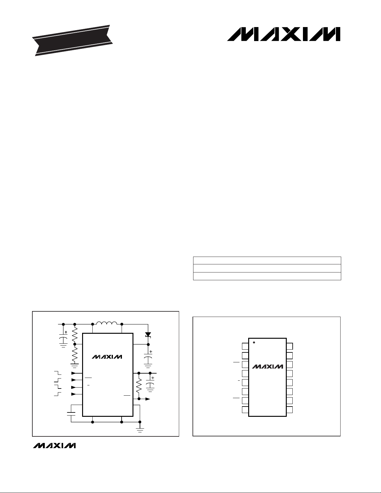
__________________Pin Configuration
MAX1672
IN
ONA
PGI
ONB
OFF
ON
PGND GND
PS
3.3V/5V
OUTPUT
INPUT
1.8V TO 11V
LOW-BATTERY
DETECTOR
OUTPUT
OUT
PG0
FB
REF
LX
OFF
3/5
ILIM
5V
0.8A
ON
3.3V
0.5A
__________Typical Operating Circuit
PART
MAX1672C/D
MAX1672EEE -40°C to +85°C
0°C to +70°C
TEMP. RANGE PIN-PACKAGE
Dice*
16 QSOP
Page 2
MAX1672
Step-Up/Down DC-DC Converter
in QSOP Package
2 _______________________________________________________________________________________
ABSOLUTE MAXIMUM RATINGS
ELECTRICAL CHARACTERISTICS
(VPS= 6V, C
REF
= 0.1µF, C
OUT
= 4.7µF, TA= -40°C to +85°C, unless otherwise noted. Typical values are at TA= +25°C.) (Note 1)
Stresses beyond those listed under “Absolute Maximum Ratings” may cause permanent damage to the device. These are stress ratings only, and functional
operation of the device at these or any other conditions beyond those indicated in the operational sections of the specifications is not implied. Exposure to
absolute maximum rating conditions for extended periods may affect device reliability.
IN, PS, LX, OUT, PGO to GND ......................... -0.3V to +11.5V
ILIM, ONA, ONB, FB, 3/5,
REF, PGI to GND......................................-0.3V to (V
PS
+ 0.3V)
PGND to GND .......................................................-0.3V to +0.3V
OUT Short Circuit to GND..........................................Continuous
Output Current..................................................................350mA
Continuous Power Dissipation (T
A
= +70°C)
16-Pin QSOP (derate above +70°C by 8.3mW/°C).......667mW
Operating Temperature Range ......................... -40°C to +85°C
Junction Temperature ....................................................+150°C
Storage Temperature Range ........................... -65°C to +160°C
Lead Temperature (soldering, 10sec)............................ +300°C
VPS= 5.5V
V
OUT
= 0V, ONA = GND, ONB = PS
VPS= 2.7V, I
OUT
= 50mA
VPS= 5.5V, I
OUT
= 50mA
ILIM = GND
VLX= 11V, ONA = GND, ONB = PS
VPS= 2.7V, ILX= 50mA
I
REF
= 0mA
VPS= 5.5V, ILX= 50mA
VIN= GND to 11V
ONA = GND, ONB = PS, current measured into PS pin
ONA = PS or ONB = GND, current measured into PS pin,
I
OUT
= 0mA
VIN= 2V, 3/5 = GND, FB = GND, I
OUT
= 10mA to 150mA
VFB= 1.3V
VIN= 3V to 5V, 3/5 = GND, I
OUT
= 100mA
Hysteresis = 15mV typical
CONDITIONS
A0.35 0.7 1.4Output PFET Current Limit
µA0.1 1Output PFET Leakage Current
Ω
2.3 4.6
1.2 2.4
Output PFET Resistance
0.3 0.5 0.7
0.35 0.5 0.65
µA0.1 1LX Leakage Current
Ω
0.9 2.0
LX On-Resistance
0.6 1.3
µA3 6IN Input Current
nA1 50FB Input Current
mV70FB Dual-Mode Trip Threshold
4.8 5.2
V0.9
V1.8 11.0Input Voltage
Startup Voltage
1.21 1.25 1.29
V1.21 1.25 1.29Reference Voltage
µA0.1 1Shutdown Quiescent Current
µA85 125Quiescent Current
4.75 5.00 5.25
V1.25 5.5
Output Voltage Adjustment
Range
%/mA0.003Output Load Regulation
%/V0.15Output Line Regulation
UNITSMIN TYP MAXPARAMETER
V
3.17 3.43
3.13 3.30 3.47
Output Voltage
FB = GND,
I
OUT
= 0mA to
150mA
TA= 0°C to +85°C
TA= -40°C to +85°C
TA= 0°C to +85°C
TA= -40°C to +85°C
V
1.20 1.30
FB Voltage
TA= 0°C to +85°C
TA= -40°C to +85°C
ILIM = PS
A
0.5 0.8 1.1
LX Current Limit
0.6 0.8 1.0
TA= 0°C to +85°C
TA= -40°C to +85°C
TA= 0°C to +85°C
TA= -40°C to +85°C
3/5 = PS
OUT = FB
3/5 = GND
Page 3
MAX1672
Step-Up/Down DC-DC Converter
in QSOP Package
_______________________________________________________________________________________ 3
ELECTRICAL CHARACTERISTICS (continued)
(VPS= 6V, C
REF
= 0.1µF, C
OUT
= 4.7µF, TA= -40°C to +85°C, unless otherwise noted. Typical values are at TA= +25°C.) (Note 1)
Note 1: Specifications to -40°C are guaranteed by design.
ONA, ONB, 3/5; ILIM
TA= 0°C to +85°C
V
PGO
= 11V
I
PGO
= 2mA, V
PGI
= 1.2V
CONDITIONS
mV30Hysteresis
°C20
°C150Thermal Shutdown Threshold
Thermal Shutdown Hysteresis
V0.4Input Low Voltage
1.21 1.29
µA0.1 1
PGO Output Leakage
V0.1 0.4
PGO Output Low Voltage
UNITSMIN TYP MAXPARAMETER
ONA, ONB, 3/5; ILIM
V1.6Input High Voltage
__________________________________________Typical Operating Characteristics
(TA = +25°C, unless otherwise noted.)
100
50
0.1 1 10 100 1000
EFFICIENCY vs. OUTPUT CURRENT
(V
OUT
= 5V)
60
MAX1672-01
OUTPUT CURRENT (mA)
EFFICIENCY (%)
70
80
90
VIN = 5V
VIN = 3.6V
VIN = 1.8V
VIN = 0.9V
VIN = 2.7V
100
50
0.1 1 10 100 1000
EFFICIENCY vs. OUTPUT CURRENT
(V
OUT
= 3.3V)
60
MAX1672-02
OUTPUT CURRENT (mA)
EFFICIENCY (%)
70
80
90
VIN = 3.3V
VIN = 1.8V
VIN = 0.9V
VIN = 2.7V
50
60
70
80
90
100
0 4 52 31 6 7 8 9 10
EFFICIENCY vs. INPUT VOLTAGE
(I
OUT
= 10mA)
MAX1672-03
INPUT VOLTAGE (V)
EFFICIENCY (%)
V
OUT
= 3.3V
V
OUT
= 5V
V
PGI
= 1.3V nA1 50PGI Input Bias Current
ONA, ONB, 3/5, ILIM
nA1 100Input Bias Current
TA= -40°C to +85°C
V
1.19 1.25 1.31
PGI Threshold Voltage
PGI/PGO COMPARATOR
LOGIC AND CONTROL INPUTS
Page 4
MAX1672
Step-Up/Down DC-DC Converter
in QSOP Package
4 _______________________________________________________________________________________
_____________________________Typical Operating Characteristics (continued)
(TA = +25°C, unless otherwise noted.)
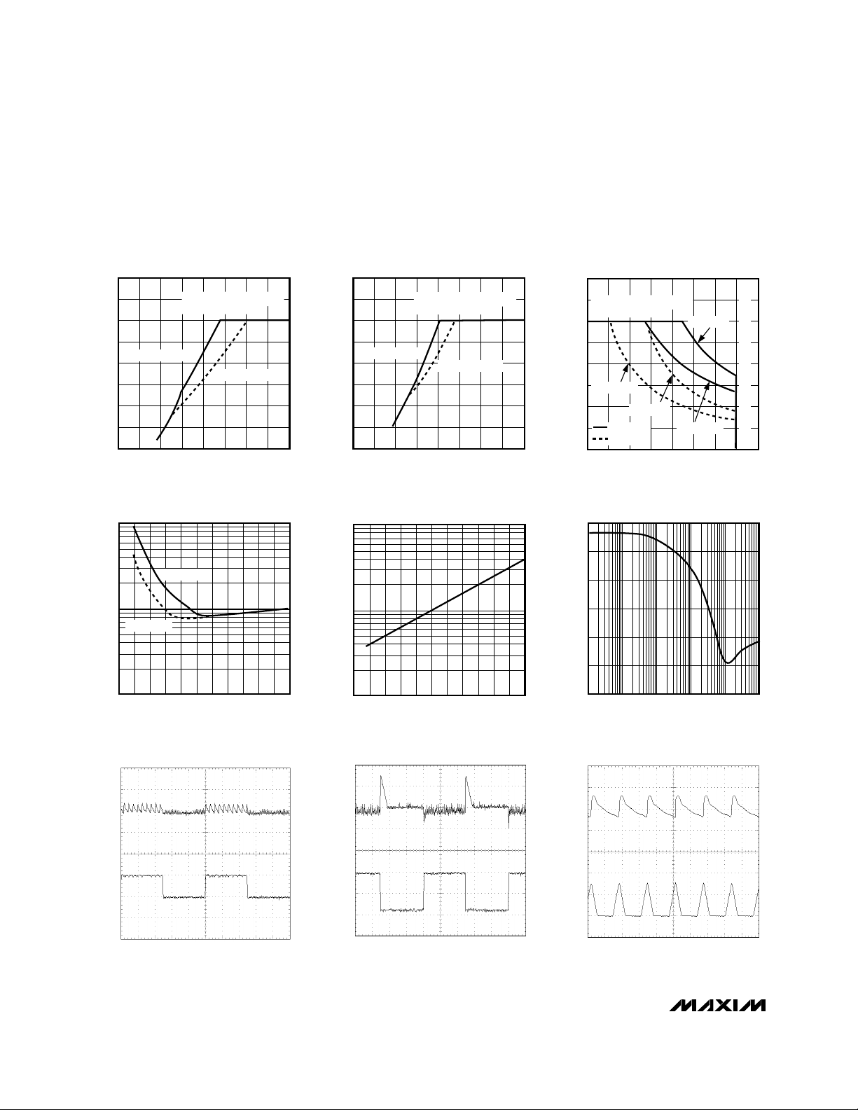
0
100
200
300
400
0 21 3 4
MAXIMUM OUTPUT CURRENT vs.
INPUT VOLTAGE (V
OUT
= 5V)
MAX1672-04
INPUT VOLTAGE (V)
MAXIMUM OUTPUT CURRENT (mA)
MAXIMUM RECOMMENDED
OUTPUT CURRENT
ILIM = GND (0.5A)
ILIM = PS (0.8A)
0
100
200
300
400
0 21 3 4
MAXIMUM OUTPUT CURRENT
vs. INPUT VOLTAGE (V
OUT
= 3.3V)
MAX1672-05
INPUT VOLTAGE (V)
MAXIMUM OUTPUT CURRENT (mA)
MAXIMUM RECOMMENDED
OUTPUT CURRENT
ILIM = GND (0.5A)
ILIM = PS (0.8A)
0
100
200
300
400
4 5 7 8 9 116 10 12
MAXIMUM OUTPUT CURRENT
vs. INPUT VOLTAGE
(POWER DISSIPATION LIMIT)
MAX1672-06
INPUT VOLTAGE (V)
MAXIMUM OUTPUT CURRENT (mA)
MAXIMUM RECOMMENDED
OUTPUT CURRENT
V
OUT
= 5V
V
OUT
= 3.3V
TA = +25°C
T
A
= +85°C
V
OUT
= 3.3V
V
OUT
= 5V
MAXIMUM RECOMMENDED INPUT VOLTAGE
1000
10
0 1 2 3 4 5 6 7 8 9 10 11
NO-LOAD BATTERY CURRENT
vs. INPUT VOLTAGE
MAX1672-07
INPUT VOLTAGE (V)
SUPPLY CURRENT (µA)
100
V
OUT
= 5V
V
OUT
= 3.3V
A
B
2ms/div
LINE-TRANSIENT RESPONSE
MAX1672-10
A: V
OUT
= 5V (100mV/div, AC COUPLED)
B: V
IN
= 2V TO 4V (I
OUT
= 100mA)
1
0.01
0 1 2 3 4 5 6 7 8 9 10 11
SHUTDOWN CURRENT
vs. INPUT VOLTAGE
MAX1672-08
INPUT VOLTAGE (V)
SUPPLY CURRENT (µA)
0.1
70
10
0.01 1 10 1000.1 1000
LINEAR REGULATOR POWER-SUPPLY
REJECTION RATIO vs. FREQUENCY
20
MAX1672-09
FREQUENCY (kHz)
PSRR (dB)
30
40
60
50
A
B
2ms/div
LOAD-TRANSIENT RESPONSE
MAX1672-11
A: V
OUT
= 5V (50mV/div, AC COUPLED)
B: I
OUT
= 10mA TO 100mA (VIN = 2V)
A
B
10µs/div
OUTPUT RIPPLE (MEDIUM LOAD)
MAX1672-12
A: V
OUT
= 5V (20mV/div, AC COUPLED)
B: I
L1
(500mA /div) (VIN = 2.7V, I
OUT
= 80mA)
Page 5

MAX1672
Step-Up/Down DC-DC Converter
in QSOP Package
_______________________________________________________________________________________ 5
______________________________________________________________Pin Description
NAME FUNCTION
1 LX Inductor Connection to the Drain of the Internal N-Channel Power MOSFET
PIN
_____________________________Typical Operating Characteristics (continued)
(TA = +25°C, unless otherwise noted.)
A
B
10µs/div
OUTPUT RIPPLE (HEAVY LOAD)
MAX1672-13
A: V
OUT
= 5V (20mV/div, AC COUPLED)
B: I
L1
(500mA /div) (VIN = 2.7V, I
OUT
= 250mA)
A
B
50µs/div
START-UP DELAY
MAX1672-14
A: V
OUT
= (2V/div)
B: ONB (2V/div) (V
IN
= 2.7V, R
LOAD
= 50Ω)
A
B
200µs/div
TURN-OFF DELAY
MAX1672-15
A: V
OUT
= (2V/div)
B: ONB (2V/div) (V
IN
= 2.7V, R
LOAD
= 50Ω)
2 PGND Power Ground
3
ONB
On Control Input. When ONB = low or ONA = high, the IC is on. Connect ONB to GND for normal operation
(Table 1).
4 ONA
On Control Input. When ONA = low and ONB = high, the IC is off. Connect ONA to PS for normal operation
(Table 1).
5
3/5
Output Voltage Selection Input. Connect to PS for 3.3V output and to GND for 5V output. With VFB> 80mV,
the state of the 3/5 pin is ignored. (Table 2).
6 PGI Low-Battery Detector Input (1.25V threshold)
7
PGO Low-Battery Detector Output (open drain). PGO pulls low when V
PGI
is greater than 1.25V.
8 ILIM Inductor-Current-Limit Selection Input. Connect to PS for 0.8A current limit and to GND for 0.5A current limit.
9 OUT Regulator Output. Drain of internal PFET linear regulator. Bypass with a 4.7µF capacitor to GND.
10 FB
Feedback Input. For 3.3V or 5V output, connect to GND. For adjustable output, connect to feedback resistordivider network. With V
FB
> 70mV, the state of the 3/5 pin is ignored.
11 PS
Bootstrapped Power Supply. Output of step-up switch-mode regulator and source of internal PFET linear
regulator. The IC is powered from this pin.
12 IN Input Voltage Sense Input. Connect to input supply.
13 REF Reference Voltage Output. Bypass with a 0.1µF capacitor to GND.
14 GND Analog Ground
15 PGND Power Ground
16 LX Inductor Connection to the Drain of the Internal N-Channel Power MOSFET
Page 6

MAX1672
Step-Up/Down DC-DC Converter
in QSOP Package
6 _______________________________________________________________________________________
N
LX
ILIM
PGND
PS
OUT
100mV
MAX1672
∆T
ON
FIXED T
OFF
GENERATOR
DRV
REF
ERROR
AMP 2
ERROR
AMP 1
INPUT
MONITOR
CURRENT-LIMIT
COMPARATOR
OFF
FB
REFERENCE
GENERATOR
P
FB
FB1
FB2
REF + OFFSET
REF
PS
N
REF
PGI
PGO
3/5
FB
REF
ONB
ONA
IN
OUT
70mV
N
GND
Figure 1. Functional Diagram
Page 7

MAX1672
Step-Up/Down DC-DC Converter
in QSOP Package
_______________________________________________________________________________________ 7
_______________Detailed Description
The MAX1672 integrates a step-up, switch-mode DCDC converter with a linear regulator to provide stepup/down voltage conversion. The step-up converter
contains an N-channel power MOSFET switch, while
the linear regulator contains a P-channel MOSFET pass
element (Figure 1). The step-up converter and the linear regulator share the same precision voltage reference. The MAX1672’s input range is from +1.8V to
+11V, and the regulated output is internally preset to
+3.3V or +5V, or can be adjusted with two external
resistors. Boost efficiency typically exceeds 80% over a
2mA to 200mA load range. The device is bootstrapped
with chip power derived from the stepped-up voltage
output at PS. The MAX1672 typically starts up with a
0.9V input.
The MAX1672’s step-up/linear-regulator configuration
permits the use of a physically smaller inductor than
competing SEPIC and flyback configurations because
the 1/2LI2requirements of a step-up converter are half
those of SEPIC and flyback converters. Also, high-frequency switching and selectable peak inductor current
limit allow for low inductor value (10µH) and low current
saturation rating, respectively, further reducing the
inductor’s physical dimensions.
The MAX1672 maximizes efficiency in both step-up and
step-down operation. In step-up mode, when VIN<
V
OUT
, only the step-up regulator is active, while the linear regulator behaves as a 1.2Ω (at 5V output) PFET
switch. This provides optimum efficiency (typically
85%).
In low-dropout, step-down operation, when VINis slightly greater than V
OUT
, both the step-up regulator and
linear regulator are active. The step-up regulator is
automatically enabled to maintain headroom across the
linear regulator (typically 1V above the 5V output). In
this case, boost ripple is rejected by the linear regulator, and OUT remains in regulation with no dropout.
In normal step-down operation, when VINis significantly
greater than V
OUT
, only the linear regulator is active.
The mode of operation is automatically controlled onchip through the IN pin, which compares VINand
V
OUT
. Transitions between step-up, low-dropout stepdown, and normal step-down operation are stable, but
can be seen as small variations in the output DC level
and output ripple.
Step-Up Switch-Mode Converter
A pulse-frequency-modulation (PFM) control scheme,
with a constant 1µs off-time and variable on-time, controls the N-channel MOSFET switch. A pulse is initiated
whenever OUT falls out of regulation. The N-channel
switch then turns off when the inductor current reaches
the peak current limit or after the 4µs maximum on-time,
whichever occurs first. This control architecture provides high-efficiency, discontinuous inductor current
under light loads as well as continuous inductor current
under heavy loads. The switching frequency and output
ripple are a function of load current and input voltage.
Linear Regulator
The low-dropout linear regulator consists of a reference, an error amplifier, and a P-channel MOSFET. The
reference is connected to the error amplifier input. The
error amplifier compares this reference with the selected feedback voltage and amplifies the difference. The
difference is conditioned and applied to the P-channel
pass transistor’s gate.
ILIM
The current-limit-select input, ILIM, selects between the
two peak inductor current limits: 0.8A (ILIM = PS) and
0.5A (ILIM = GND). If the application requires low output current (see
Typical Operating Characteristics
),
select 0.5A. The lower peak current limit allows for a
smaller, lower-cost inductor, and reduced output ripple.
On/Off Control
The MAX1672 is turned on or off by logic inputs ONA
and ONB (Table 1). When ONA = 1 or ONB = 0, the
device is on. When ONA = 0 and ONB = 1, the device
shuts down (see the
Applications Information
section).
For normal (on) operation, connect ONA to PS and
ONB to GND. Shutdown mode turns off the MAX1672
completely, disconnecting the input from the output
and actively pulling OUT to GND.
ONB
MAX1672
0 0 On
0 1 Off
ONA
1 0 On
1 1 On
Table 1. On/Off Logic Control
Page 8

MAX1672
Step-Up/Down DC-DC Converter
in QSOP Package
8 _______________________________________________________________________________________
__________________Design Procedure
Output Voltage Selection
For fixed output voltages of 3.3V or 5V, connect 3/5 to
PS or GND and connect FB to GND (Table 2).
Alternatively, adjust the output voltage from 1.25V to
5.5V by connecting two resistors, R1 and R2 (Figure 2),
which form a voltage divider between OUT and FB.
Choose resistor values as follows:
R1 = R2[(V
OUT
/ V
REF
) -1]
where V
REF
= 1.25V. Since the input bias current at FB
has a maximum value of 50nA, R1 and R2 can be large
with no significant accuracy loss. Choose R2 in the
100kΩ to 270kΩ range and calculate R1 using the
above formula. For 1% error, the current through R1
should be at least 100 times FB’s bias current.
Whenever the voltage at FB exceeds 70mV above
GND, the state of the 3/5 pin is ignored. Connect 3/5 to
GND when adjusting V
OUT
with a resistor divider. Never
leave 3/5 unconnected.
Low-Battery Detection
The MAX1672 contains a comparator for low-battery
detection. If the voltage at PGI falls below V
REF
(typically 1.25V), the open-drain comparator output (PGO)
goes high. Hysteresis is typically 30mV. Set the lowbattery detector’s threshold with resistors R3 and R4
(Figure 2) using the following equation:
R3 = R4[(V
PGT
/ V
REF
) -1]
where V
PGT
is the desired threshold of the low-battery
detector and V
REF
= 1.25V. Since the input bias current
at PGI has a maximum value of 50nA, R3 and R4 can
be large to minimize input loading with no significant
accuracy loss. Choose R4 in the 100kΩ to 270kΩ range
and calculate R3 using the above formula. For 1%
error, the current through R3 should be at least 100
times PGI’s bias current.
The PGO output is open-drain and should be pulled
high with external resistor R5 for normal operation. If the
low-battery comparator is not used, connect PGI and
PGO to GND.
Inductor Selection
A 10µH inductor performs well in most MAX1672 applications. Smaller inductor values typically offer a smaller
physical size for a given series resistance, but may
increase switching losses. Larger inductor values
exhibit higher output current capability and larger physical dimensions for a given series resistance. For optimum performance, choose an inductor value from
Table 3 or by using the following equation:
where I
LIM
is the peak switch-current limit, which is
0.8A for I
LIM
= PS and 0.5A for I
LIM
= GND.
The inductor’s incremental saturation current rating
should also be greater than the peak switch-current
limit. However, it is generally acceptable to bias most
inductors into saturation by as much as 20% with slightly reduced efficiency. The inductor’s DC resistance significantly affects efficiency. See Tables 4 and 5 for a list
of suggested inductors and suppliers.
V + V
I
V + V
I
OUT DIODE
LIM
IN(min) SWITCH
LIM
( )
<
<
( )
t L
t
OFF
ON
2
(max)
MAX1672
IN
ONA
PGI
ONB
OFF
ON
C3
0.1µF
C1
100µF
C2
100µF
R2
R1
R5
1M
C4
4.7µF
R3
R4
L1
10µH
PGND GND
PS
1.25V TO
5.5V OUTPUT
INPUT
1.8V TO 11V
LOW-BATTERYDETECTOR
OUTPUT
OUT
PG0
FB
REF
LX
OFF
3/5
ILIM
0.8A
ON
0.5A
Figure 2. Adjustable Output Voltage Configuration
Table 2. Output Voltage Control
FB V
OUT
(V)
0 GND +5
1 GND +3.3
3/
55
X >70mV +1.25 to +5.5
Page 9

MAX1672
Step-Up/Down DC-DC Converter
in QSOP Package
_______________________________________________________________________________________ 9
Capacitor Selection
The equivalent series resistance (ESR) of both bypass
and filter capacitors affects efficiency and output ripple. Output voltage ripple is the product of peak inductor current and filter capacitor ESR. Use low-ESR
capacitors for best performance, or connect two or
more filter capacitors in parallel.
A 100µF, 16V, input bypass capacitor (C1) with low
ESR reduces peak battery currents and reflected noise
due to inductor current ripple. Smaller ceramic capacitors may also be used for light loads or in applications
that can tolerate higher input ripple.
A 100µF, 16V, surface-mount (SMT) tantalum PS filter
capacitor (C2) with 0.1Ω ESR typically exhibits 20mV
output ripple (at OUT) when stepping up from 2V to 5V
at 100mA load. Smaller capacitors (down to 10µF with
higher ESR) are acceptable for light loads or in applications that can tolerate higher output ripple.
Only 4.7µF is needed at OUT (C4) to maintain linear
regulator stability. During boost operation, this capacitor reduces output voltage spikes from the step-up converter by forming an R-C lowpass filter along with the
P-channel MOSFET on-resistance. Output ripple can be
further reduced by increasing C4.
See Tables 4 and 5 for a list of suggested capacitors
and suppliers.
Diode Selection
The MAX1672’s high switching frequency demands a
high-speed rectifier. Schottky diodes, such as the
1N5817 or MBRS130T3, are recommended. Make sure
the diode’s current rating exceeds the maximum load
current. See Tables 4 and 5 for a list of suggested
diodes and suppliers.
Table 3. Suggested Inductor Values Table 4. Suggested Components
ILIM
INDUCTOR VALUE
(µH)
0 (5V) 0 (0.5A) 10 to 22
0 (5V) 1 (0.8A) 10
3/
55
1 (3.3V) 0 (0.5A) 10
1 (3.3V) 1 (0.8A) 4.7 to 10
INDUCTORS
Sumida
CD43-100 (1.04A, 0.182Ω)
CD54-100 (1.44A, 0.100Ω)
CDRH73-100 (1.68A, 0.072Ω)
L1
10µH
Coilcraft
DT1608C-103 (0.7A, 0.095Ω)
CAPACITORS
AVX
TPSE Series
Sprague
593D or 595D Series
Tantalum
DIODES
Motorola
MBRS130LT3 (1.0A, 30V)
MBR0520LT3 (0.5A, 20V)
Schottky
1N5817 Equivalent
International Rectifier
10BQ40 (1.0A, 40V)
Table 5. Component Suppliers
PHONE
AVX (803) 946-0690
Coilcraft (847) 639-6400
SUPPLIER
International
Rectifier
(310) 322-3331
Motorola (602) 303-5454
FAX
(803) 626-3123
(847) 639-1469
(310) 322-3332
(602) 994-6430
Sanyo (619) 661-6835 (619) 661-1055
Sprague (603) 224-1961 (603) 224-1430
Sumida (847) 956-0666 (847) 956-0702
Page 10

MAX1672
Step-Up/Down DC-DC Converter
in QSOP Package
10 ______________________________________________________________________________________
__________Applications Information
Using a Single, Pushbutton On/Off Switch
A single pushbutton switch can be used to turn the
MAX1672 on and off. As shown in Figure 3, ONA is
pulled low and ONB is pulled high when the part is off.
When the momentary switch is pressed, ONB is pulled
low and the regulator turns on. The switch should be on
long enough for the µC to exit reset. The controller
issues a logic high to ONA, which guarantees the part
will stay on regardless of the switch state.
To turn off the regulator, press the switch again. The
controller reads the switch status and pulls ONA low.
When the switch is released, ONB goes high, turning
off the MAX1672.
Thermal Overload Protection
Thermal overload protection limits total power dissipation in the MAX1672. When the junction temperature
exceeds TJ= +150°C, the pass transistor turns off,
allowing the MAX1672 to cool. The pass transistor turns
on again after the IC’s junction temperature cools by
20°C, resulting in a pulsed output during thermal overload conditions.
Thermal overload protection is designed to protect the
MAX1672 if fault conditions occur. It is not intended to
be used as an operating mode. Prolonged operation in
thermal shutdown mode may reduce the IC’s reliability.
For continual operation, do not exceed the absolute
maximum junction temperature rating TJ= +150°C.
Power Dissipation and Operating Region
The MAX1672’s maximum power dissipation in stepdown mode depends on the thermal resistance of the
case and circuit board, the temperature difference
between the die junction and ambient air, and the air
flow rate. The power dissipated in the device is
P = I
OUT(VIN
- V
OUT
) during step-down operation. The
maximum power dissipation is as follows:
P
MAX
= (TJ- TA)/(θ
JB
+ θBA)
where (TJ- TA) is the temperature difference between
the MAX1672 die junction and the surrounding air, θ
JB
(or θJC) is the thermal resistance of the package, and
θBAis the thermal resistance throughout the printed cir-
cuit board, copper traces, and other materials to the
surrounding air. The MAX1672’s thermal resistance is
120°C/W. See the
Typical Operating Characteristics
for
Maximum Output Current vs. Input Voltage.
Layout Considerations
Proper PC board layout is essential to minimize noise
due to high inductor current levels and fast switching
waveforms. To maximize output power and efficiency
and minimize output ripple voltage and ground noise,
use the following guidelines when designing your
board:
• Use a ground plane.
• Keep the IC’s GND pin and the ground leads of C1
and C2 (Figure 2) less than 0.2in. (5mm) apart.
• Make all connections to the FB and LX pins as short
as possible.
• Solder the IC’s GND pin directly to the ground
plane.
Refer to the MAX1672 EV kit for a suggested PC board
layout.
MAX1672
ONA
ONB
1M
1M
I/O
I/O
OUT
V
DD
µ
C
Figure 3. Momentary Pushbutton On/Off Control
Page 11

MAX1672
Step-Up/Down DC-DC Converter
in QSOP Package
______________________________________________________________________________________ 11
________________________________________________________Package Information
QSOP.EPS
Page 12

MAX1672
Step-Up/Down DC-DC Converter
in QSOP Package
12 ______________________________________________________________________________________
NOTES
 Loading...