

Page 1
For free samples & the latest literature: http://www.maxim-ic.com, or phone 1-800-998-8800.
For small orders, phone 1-800-835-8769.
General Description
The MAX1669 fan controller includes a precise digital
thermometer that reports the temperature of a remote
sensor. The remote sensor is a diode-connected transistor—typically a low-cost, easily mounted 2N3906 PNP
type—replacing conventional thermistors or thermocouples. Remote accuracy is ±3°C for transistors from multiple manufacturers, with no calibration needed. The
MAX1669 has an independent fan controller with a lowcurrent logic output requiring external power components to interface to a DC brushless fan. The fan
controller has two modes of operation: a low-frequency
(20Hz to 160Hz) PWM mode intended for driving the fan
motor, or a high-impedance DAC output that generates
a variable DC control voltage. In PWM mode, the FAN
frequency can be synchronized to an external clock.
Other key features include general-purpose inputs/outputs (GPIOs) for fan presence detection and a thermostat output intended as a fan override signal in case the
host system loses the ability to communicate. The internal ADC has a wide input voltage range and gives
overrange readings when too large an input voltage is
applied. Other error-checking includes temperature
out-of-range indication and diode open/short faults.
The MAX1669 is available in a space-saving 16-pin
QSOP package that allows it to fit adjacent to the
SLOT1 connector.
Applications
Pentium®CPU Cooling
Desktop Computers
Notebook Computers
Servers
Workstations
Features
♦ Measures Remote CPU Temperature
♦ No Calibration Required
♦ 20Hz to 160Hz PWM Output for Fan
♦ PWM Frequency Sync Input (260kHz)
♦ Flexible Fan Interface: Linear or PWM
♦ SMBus 2-Wire Serial Interface
♦ Programmable Under/Overtemperature Alarms
♦ ALERT Latched Interrupt Output
♦ OVERT Thermostat Output
♦ Two GPIO Pins
♦ Write-Once Configuration Protection
♦ Supports SMBus Alert Response
♦ ±3°C Temperature Accuracy (-40°C to +125°C,
remote)
♦ 3µA Standby Supply Current
♦ +3V to +5.5V Supply Range
♦ Small 16-Pin QSOP Package
MAX1669
Fan Controller and Remote Temperature Sensor
with SMBus Serial Interface
________________________________________________________________ Maxim Integrated Products 1
19-1574; Rev 0; 1/00
PART
MAX1669EEE
-40°C to +85°C
TEMP. RANGE PIN-PACKAGE
16 QSOP
Pentium is a registered trademark of Intel Corp.
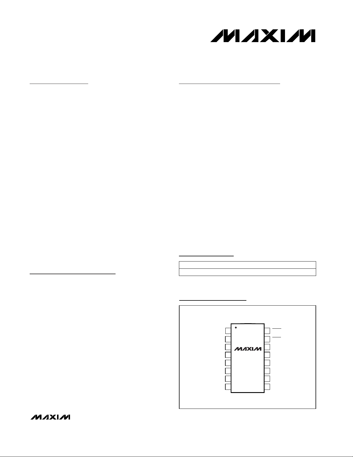
Pin Configuration
Ordering Information
Typical Operating Circuit appears at end of data sheet.
TOP VIEW
1
I/O1 OVERT
I/O2
2
ADD0
3
MAX1669
4
ADD1
ADD2
5
AGND
6
DXN
7
DXP
8
16
15
14
13
12
11
10
9
ALERT
SMBDATA
SMBCLK
PGND
FAN
SYNC
V
CC
QSOP
Page 2
MAX1669
Fan Controller and Remote Temperature Sensor
with SMBus Serial Interface
2 _______________________________________________________________________________________
ABSOLUTE MAXIMUM RATINGS
ELECTRICAL CHARACTERISTICS
(VCC= +3.3V, TA= 0°C to +85°C, unless otherwise noted. Typical values are at TA= +25°C.)
Stresses beyond those listed under “Absolute Maximum Ratings” may cause permanent damage to the device. These are stress ratings only, and functional
operation of the device at these or any other conditions beyond those indicated in the operational sections of the specifications is not implied. Exposure to
absolute maximum rating conditions for extended periods may affect device reliability.
VCCto AGND...........................................................-0.3V to +6V
DXP, ADD_ to AGND.................................-0.3V to (V
CC
+ 0.3V)
DXN to AGND.......................................................-0.3V to +0.8V
SMBCLK, SMBDATA, ALERT, SYNC,
I/O1, I/O2, OVERT, FAN to AGND ......................-0.3V to +6V
FAN to PGND ............................................-0.3V to (V
CC
+ 0.3V)
PGND to AGND ....................................................-0.3V to +0.3V
PWM Current....................................................-50mA to +50mA
SMBDATA Current .............................................-1mA to +50mA
I/O1, I/O2 Current...............................................-1mA to +25mA
DXN Current ......................................................................±1mA
ESD Protection (all pins, Human Body Model) .................2000V
Continuous Power Dissipation (T
A
= +70°C)
16-Pin QSOP (derate 8.30mW/°C above +70°C).......667mW
Operating Temperature Range (extended)......-55°C to +125°C
Junction Temperature.....................................................+150°C
Storage Temperature Range ............................-65°C to +150°C
Lead Temperature (soldering, 10s) ................................+300°C
FAN output set to
DAC mode
FAN output set to
150Hz mode
TR= 0°C to +100°C, diode ideality factor = 1.013
High level
PWM mode, V
FAN
forced to 0.4V
PWM mode, V
FAN
forced to 2.9V
Monotonicity guaranteed
V
DXP
forced to V
DXN
+ 0.65V
SMBus static
Autoconvert mode
From stop bit to conversion complete
VCC, falling edge
VCCinput, disables A/D conversion,
rising edge
Autoconvert mode,
average measured over 1s
CONDITIONS
mA
-10
FAN Output Sink Current
mA
10
FAN Output Source Current
V
0.7
DXN Source Voltage
80 100 120
µARemote-Diode Source Current
Hz
1.6 2 2.4
Conversion Rate
ms
47 62 78
Conversion Time
µA
360
µA
75 150
Average Operating Supply Current
°CTemperature Error, Remote Diode (Note 2)
Bits
8
Resolution (Note 1)
310
µAStandby Supply Current
mV
50
POR Threshold Hysteresis
V
1 1.9 2.5
Power-On Reset Threshold
-3 3
V
3 5.5
Supply Voltage Range
V
2.6 2.8 2.95
Undervoltage Lockout Threshold
mV
50
Undervoltage Lockout Hysteresis
UNITSMIN TYP MAXPARAMETER
SMBCLK at 10kHz
3
Low level
81012
ADC AND POWER SUPPLY
FAN OUTPUT
Page 3
MAX1669
Fan Controller and Remote Temperature Sensor
with SMBus Serial Interface
_______________________________________________________________________________________ 3
ELECTRICAL CHARACTERISTICS (continued)
(VCC= +3.3V, TA= 0°C to +85°C, unless otherwise noted. Typical values are at TA= +25°C.)
Logic Input High Voltage
PARAMETER MIN TYP MAX UNITS
FAN PWM Frequency Error
-20 +20
%
FAN Total Unadjusted Error
-4 4
%FS
FAN Output Voltage High
2.96 3.06
V
CONDITIONS
PWM mode, any setting
DAC mode, any setting, RL= 10kΩ to GND
DAC mode, FAN duty factor = 1111b,
I
OUT
= 5mA
SYNC Input Low Period
500
ns
SYNC Input High Period
500
ns
SYNC Capture Range
140 260 400
kHz
2.1
V
Logic Input Low Voltage
0.8
V
SMBDATA, ALERT, OVERT, I/O1, I/O2
Output Low Sink Current
6
mA
FAN Output Voltage Low
0.05 0.2
V
ALERT, OVERT, I/O1, I/O2 Output
High Leakage Current
1
µA
Logic Input Current
-1 1
µA
SMBus Input Capacitance
5
pF
SMBus Clock Frequency
DC 100
kHz
SMBCLK Clock Low Time (t
LOW
)
4.7
µs
SMBCLK Clock High Time (t
HIGH
)
4
µs
SMBus Rise Time
1
µs
SMBus Fall Time
300
ns
SMBus Start Condition Setup Time
4.7
µs
SMBus Repeated Start Condition Setup
Time (t
SU:STA
)
500
ns
SMBus Start Condition Hold Time (t
HD:STA
)
4
µs
SMBus Stop Condition Setup Time (t
SU:STO
)
4
µs
SMBus Data Valid to SMBCLK
Rising-Edge Time (t
SU:DAT
)
250
ns
Pin forced to 5.5V
Logic inputs forced to VCCor GND
ADD_, I/O1, I/O2, SYNC, SMBCLK, SMBDATA;
VCC= 3V to 5.5V
ADD_, I/O1, I/O2, SYNC, SMBCLK, SMBDATA;
VCC= 3V to 5.5V
SMBCLK, SMBDATA
(Note 3)
Pin forced to 0.4V
10% to 10% points
90% to 90% points
SMBCLK, SMBDATA, 10% to 90% points
SMBCLK, SMBDATA, 90% to 10% points
90% to 90% points
DAC mode, FAN duty factor = 0000b,
I
OUT
= -5mA
10% of SMBDATA to 90% of SMBCLK
90% of SMBCLK to 10% of SMBDATA
10% or 90% of SMBDATA to 10% of SMBCLK
SMBus Data-Hold Time (t
HD:DAT
)
0
µs
SMBus Bus-Free Time (t
BUF
)
4.7
µs
SMBCLK Falling Edge to SMBus
Data-Valid Time
1
µs
(Note 4)
Between start/stop conditions
Master clocking-in data
SMBus INTERFACE (Figures 7, 8)
Page 4
Note 1: Guaranteed but not 100% tested.
Note 2: T
R
is the junction temperature of the remote diode. The temperature error specification is optimized to and guaranteed for a
diode-connected 2N3906 transistor with ideality factor = 1.013. Variations in the ideality factor “m” of the actual transistor
used will increase the temperature error by *. See the Temperature Error vs. Remote Diode Temperature graph in the
Typical Operating Characteristics for typical temperature errors using several random 2N3906s. See Remote Diode
Selection for remote diode forward-voltage requirements.
Note 3: The SMBus logic block is a static design that works with clock frequencies down to DC. While slow operation is possible, it
violates the 10kHz minimum clock frequency and SMBus specifications, and may monopolize the bus.
Note 4: Note that a transition must internally provide at least a hold time in order to bridge the undefined region (300ns max) of
SMBCLK’s falling edge.
Note 5: Specifications to -40°C are guaranteed by design and not production tested.
MAX1669
Fan Controller and Remote Temperature Sensor
with SMBus Serial Interface
4 _______________________________________________________________________________________
ELECTRICAL CHARACTERISTICS
(VCC= +3.3V, TA= -40°C to +85°C, unless otherwise noted.) (Note 5)
Pin forced to 0.4V
ADD_, I/O1, I/O2, SYNC, SMBCLK, SMBDATA;
VCC= 3V to 5.5V
ADD_, I/O1, I/O2, SYNC, SMBCLK, SMBDATA;
V
CC
= 3V to 5.5V
Logic inputs forced to VCCor GND
Pin forced to 5.5V
µA
-1 1
Logic Input Current
µA
1
ALERT, OVERT, I/O1, I/O2 Output
High Leakage Current
V
0.2
FAN Output Voltage Low
mA
6
SMBDATA, ALERT, OVERT, I/O1, I/O2
Output Low Sink Current
V
0.8
Logic Input Low Voltage
V
2.1
Logic Input High Voltage
DAC mode, FAN duty factor = 1111b,
I
OUT
= 5mA
DAC mode, any setting, RL= 10kΩ to GND
PWM mode, any setting
PWM mode, V
FAN
forced to 0.4V
PWM mode, V
FAN
forced to 2.9V
Monotonicity guaranteed
Autoconvert mode
From stop bit to conversion complete
TR= -55°C to +125°C, diode ideality factor = 1.013
Autoconvert mode, average measured over
1sec, FAN output set to 150Hz mode
CONDITIONS
V
2.94
FAN Output Voltage High
%FS
-5 5
FAN Total Unadjusted Error
%
-25 +25
FAN PWM Frequency Error
mA
-10
FAN Output Sink Current
mA
10
FAN Output Source Current
Hz
1.6 2.4
Conversion Rate
ms
47
Conversion Time
µA
100
Average Operating Supply Current
Bits
8
Temperature Resolution (Note 1)
°C
-5 5
Temperature Error, Remote Diode (Note 2)
UNITSMIN MAXPARAMETER
DAC mode, FAN duty factor = 0000b,
I
OUT
= -5mA
V
3 5.5
Supply Voltage Range
ADC AND POWER SUPPLY
FAN OUTPUT
SMBus INTERFACE
1 013
*
.
=−
m
1 273 15
. ∆T
()
kT C
+
°
()
R
Page 5
MAX1669
Fan Controller and Remote Temperature Sensor
with SMBus Serial Interface
_______________________________________________________________________________________ 5
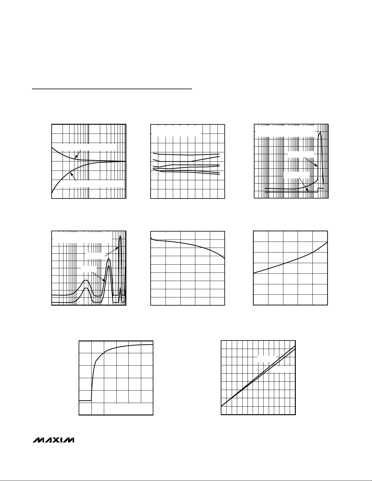
Typical Operating Characteristics
(Temperature error = measured - actual, TA= +25°C, unless otherwise noted.)
TEMPERATURE ERROR
vs. LEAKAGE RESISTANCE
40
30
20
10
-10
-20
TEMPERATURE ERROR (°C)
-30
-40
PATH = DXP TO GND; CONFIG = 02h
0
PATH = DXP TO V
1 10 100
LEAKAGE RESISTANCE (MΩ)
(5V); CONFIG = 02h
CC
TEMPERATURE ERROR vs.
COMMON-MODE NOISE FREQUENCY
8
VIN = 50mVp-p AC-COUPLED TO DXN
7
C = DXN - DXP CAPACITANCE
6
5
4
3
2
1
TEMPERATURE ERROR (°C)
0
-1
-2
1M 1G100M10M
C = 2200pF
C = 27nF
FREQUENCY (Hz)
MAX1669-01
MAX1669-04
2.0
1.5
1.0
0.5
0
-0.5
TEMPERATURE ERROR (°C)
-1.0
-1.5
-2.0
2
0
-2
-4
-6
-8
-10
TEMPERATURE ERROR (°C)
-12
-14
-16
TEMPERATURE ERROR
vs. REMOTE DIODE TEMPERATURE
RANDOM 2N3906s FROM
DIFFERENT MANUFACTURERS
-60 20-20 60 100-40 400 80 120 140
TEMPERATURE (°C)
TEMPERATURE ERROR
vs. DXP - DXN CAPACITANCE
V
= 5V
CC
02010 30 40 50
DXP-DXN CAPACITANCE (nF)
MAX1669-02
MAX1669-05
TEMPERATURE ERROR vs.
POWER-SUPPLY NOISE FREQUENCY
18
VIN = SQUARE WAVE APPLIED TO
16
14
12
10
TEMPERATURE ERROR (°C)
-2
WITH NO 0.1µF VCC CAPACITOR
V
CC
VIN = 250mVp-p
8
6
4
2
0
1K 10K 100K 1M 10M 100M
VIN = 100mVp-p
PSNF (Hz)
STANDBY SUPPLY CURRENT
vs. SUPPLY VOLTAGE
7
6
5
4
3
2
STANDBY SUPPLY CURRENT (µA)
1
0
3.0 4.03.5 4.5 5.0 5.5
SUPPLY VOLTAGE (V)
MAX1669-03
MAX1669-06
RESPONSE TO THERMAL SHOCK
120
100
80
60
TEMPERATURE (°C)
40
20
0
-2 2 406810
CMPT3906 IMMERSED IN
+115°C FLUORINERT BATH
TIME (sec)
MAX1669-07
PWM FREQUENCY vs. CODE (F3F2F1F0)
180
160
140
120
100
80
60
PWM FREQUENCY (Hz)
40
20
0
042 5 7 8 10 123169111314
V
= +5V
CC
CODE (F3F2F1F0)
V
CC
= +3.3V
MAX1669-08
Page 6
MAX1669
Fan Controller and Remote Temperature Sensor
with SMBus Serial Interface
6 _______________________________________________________________________________________
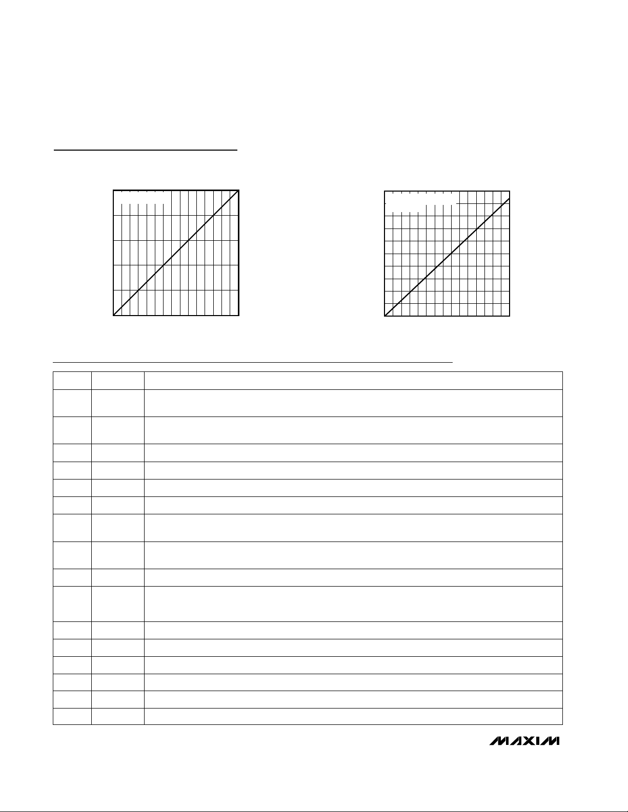
Typical Operating Characteristics (continued)
(Temperature error = measured - actual, TA= +25°C, unless otherwise noted.)
Pin Description
NAME FUNCTION
1
I/O1
General-Purpose Open-Drain Logic Input/Output 1. I/O1 is intended for driving LEDs, driving power-plane
switching MOSFETs, or detecting fan presence or chassis intrusion.
2 I/O2
General-Purpose Open-Drain Logic Input/Output 2. I/O2 is intended for driving LEDs, driving power-plane
switching MOSFETs, or detecting fan presence or chassis intrusion.
PIN
3 ADD0 SMBus Address Select Pin 0. See Table 11.
4 ADD1 SMBus Address Select Pin 1. See Table 11.
8 DXP
Combined Current Source and ADC Positive Input from Remote Diode. Place a 2200pF capacitor
between DXP and DXN for noise filtering.
7 DXN
Combined Current Sink and ADC Negative Input from Remote Diode. DXN is normally biased to a diode
voltage above ground.
6 AGND Analog Ground
5 ADD2 SMBus Address Select Pin 2. See Table 11.
13 SMBCLK SMBus Serial-Clock Input
12 PGND Power Ground
11 FAN
Fan-Control Logic Output. Swings from PGND to VCCin PWM mode, or PGND to 0.94 · VCCin DAC mode.
10 SYNC
Oscillator Synchronization Input. Connect to AGND to use internal clock. Capture range is 140kHz to
400kHz. The synchronization signal is internally applied to the FAN PWM clock. See Table 5 for synchronized frequencies.
9 V
CC
Supply Voltage Input, +3V to +5.5V. Bypass to AGND with a 0.1µF capacitor.
16
OVERT
Active-Low, Open-Drain Thermostat Output. Activated by T
CRIT
threshold
15
ALERT
Active-Low, Open-Drain SMBus Alert (interrupt) Output
14 SMBDATA Open-Drain SMBus Serial-Data Input/Output
PWM DUTY FACTOR vs. CODE (D3D2D1D0)
100
V
= +3.3V OR +5V
CC
80
60
40
DUTY FACTOR (%)
20
0
042 5 7 8 10 1231 6 9 11 131415
CODE (D3D2D1D0)
MAX1669-09
DAC OUTPUT vs. CODE (D3D2D1D0)
5.0
I
= +10mA TO -10mA
LOAD
4.5
= +5V
V
CC
4.0
3.5
3.0
2.5
2.0
DAC OUTPUT (V)
1.5
1.0
0.5
0
042 5 7 8 10 1231691114
CODE (D3D2D1D0)
13
MAX1669-10
15
Page 7

MAX1669
Fan Controller and Remote Temperature Sensor
with SMBus Serial Interface
_______________________________________________________________________________________ 7
_______________Detailed Description
The MAX1669 temperature sensor is designed to work
with an external microcontroller (µC) or other intelligent
devices in computer fan-control applications. The µC is
typically a power-management or keyboard controller,
generating SMBus serial commands by “bit-banging’’
general-purpose input/output (GPIO) pins or through a
dedicated SMBus interface block.
Essentially an 8-bit serial analog-to-digital converter
(ADC) with a sophisticated front end, the temperature
measurement channel contains a switched-current
source, a multiplexer, and an integrating ADC.
Temperature data from the ADC is loaded into a data
register, where it is automatically compared with data
previously stored in over/undertemperature alarm registers and the critical register (Figure 1).
Figure 1. MAX1669 Temperature Sensor Functional Diagram
DXP
DXN
GND
V
CC
ADD0
ADD1
ADD2
SMBDATA
SMBCLK
ALERT
MUX
8
8
COMMAND-BYTE
(INDEX) REGISTER
REMOTE-TEMPERATURE
DATA REGISTER
HIGH-TEMPERATURE
THRESHOLD
LOW-TEMPERATURE
THRESHOLD
8
DIGITAL COMPARATOR
ADC
CONTROL
LOGIC
CONFIGURATION
BYTE REGISTER
STATUS BYTE REGISTER
ALERT RESPONSE
ADDRESS REGISTER
R
SQ
ADDRESS
DECODER
SMB
READ WRITE
88
MAX1669
CONTROL
LOGIC
TEMPERATURE SENSOR
I/O1
I/O2
GENERAL-PURPOSE
I/O CONTROLLER
TEMPERATURE
T
CRIT
-5°C
OVERT
R
S
Q
CONTROL
LOGIC
Page 8

MAX1669
Fan Controller and Remote Temperature Sensor
with SMBus Serial Interface
8 _______________________________________________________________________________________
The PWM or DAC fan control circuitry is completely
independent from the temperature measurement, and
software closes the temperature-control feedback loop
(Figure 2).
ADC and Multiplexer
The ADC is an averaging type that integrates over a
62ms period (typ), with excellent noise rejection. The
multiplexer automatically steers bias currents through
the remote diode, measures the forward voltage, and
calculates the temperature.
The DXN input is biased at 0.7V above ground by an
internal diode to set up the analog-to-digital (A/D)
inputs for a differential measurement. The worst-case
DXP-DXN differential input voltage range is 0.21V to
0.95V. Diode voltages that are outside the ADC input
range cause overrange indications rather than nonmonotonic readings. Overrange readings will return
+127°C. Excess resistance in series with the remote
diode causes approximately +1/2°C error/Ω. Likewise,
200µV of offset voltage forced on DXP-DXN causes
approximately +1°C error.
A/D Conversion Sequence
When the device is taken out of standby mode, the
result of the measurement is available one conversion
time later (78ms max). If the ADC is busy, the results of
the previous conversion are always available. Toggling
the standby mode on and off is a good way to initiate a
new conversion since this action resets the rate timer.
Low-Power Standby Mode
Supply-current drain during the 62ms conversion period is 500µA. Between conversions, the instantaneous
supply current is 18µA. In standby mode, supply current drops to 3µA and the fan output is disabled.
SMBus Digital Interface
From a software perspective, the MAX1669 appears as
a set of byte-wide registers that contain temperature
data, alarm threshold values, or control bits. A standard
SMBus 2-wire serial interface is used to read temperature data and write control bits and alarm threshold
data.
The MAX1669 employs four standard SMBus protocols:
write byte, read byte, send byte, and receive byte
(Figure 3). The two shorter protocols (receive and
send) allow quicker transfers, provided that the correct
data register was previously selected by a write or read
byte instruction. Use caution with the shorter protocols
in multimaster systems since a second master could
overwrite the command byte without informing the first
master.
The temperature data format is 7 bits plus sign in two’s
complement form for each channel, with the LSB representing +1°C (Table 1), MSB transmitted first.
Measurements are offset by +1/2°C to minimize internal
rounding errors; for example, +99.5°C to +100.4°C is
reported as +100°C.
Alarm Threshold Registers
Three registers store alarm threshold data, with hightemperature (T
HIGH
) and low-temperature (T
LOW
) reg-
isters that activate the ALERT output, and a critical
overtemperature register (T
CRIT
) that activates the
OVERT output. If a measured temperature equals or
exceeds the T
HIGH
or T
LOW
threshold value, an ALERT
interrupt is asserted. Do not set the T
CRIT
register to
values outside of the temperatures in Table 1.
The power-on-reset (POR) state of the T
HIGH
register is
full scale (0111 1111b or +127°C). The POR state of the
T
LOW
register is 1100 1001b or -55°C. The POR state of
the T
CRIT
register is 0110 0100b or +100°C.
OVERT
Thermostat Output
The OVERT output is a self-clearing interrupt output
that is activated when the temperature equals or
exceeds T
CRIT
. OVERT normally goes low when active,
but this polarity can be changed through the configuration register. The latch is cleared when the temperature
reading is equal to or less than T
CRIT
minus 5°C, which
provides for 5°C of hysteresis.
The ALERT and OVERT comparisons are made after
each conversion, and at the end of a write command to
their respective temperature limit registers. For example, if the limit is changed while the device is in standby
Figure 2. MAX1669 Fan-Control Functional Diagram
FREQ
REGISTER
DUTY
REGISTER
(0XF0)
UPPER NIBBLE
4
CONTROLLER
AND
PWM
DAC
MUX
FANON
OVERT
MAX1669
DRIVER
CONTROL
LOGIC
FAN
Page 9

MAX1669
Fan Controller and Remote Temperature Sensor
with SMBus Serial Interface
_______________________________________________________________________________________ 9
mode, the ALERT and OVERT outputs respond correct-
ly according to the last valid A/D result.
Note that the ALERT output does not respond to T
CRIT
(OVERT) comparisons.
The OVERT latch can implement an override control to
the FAN output, which forces the fan to V
CC
whenever
the T
CRIT
threshold is crossed. This override switch is
the backup fan control loop, and is enabled through the
FAN ON bit in the configuration register (bit 2). Note
that changing the duty to 100% in this way doesn’t
affect the contents of the DUTY register, and the FAN
output reverts to the preprogrammed duty factor (or
DAC voltage) when the OVERT latch is reset.
Diode Fault Alarm
A continuity fault detector at DXP detects whether the
remote diode has an open-circuit condition, short-circuit to GND, or short-circuit DXP-to-DXN condition. At
the beginning of each conversion, the diode fault is
checked and the status byte updated. This fault detector is a simple voltage detector; DXP rising above VCC1V or falling below DXN + 40mV constitutes a fault condition. Also, if the ADC has an extremely low differential
input voltage, the diode is assumed to be shorted and
a fault occurs. Note that the diode fault isn’t checked
until a conversion is initiated, so immediately after
power-on reset the status byte indicates no fault is present even if the diode path is broken. Any diode fault
will return a +127°C fault reading and cause ALERT to
go low.
Write Byte Format
Read Byte Format
7-bit slave address:
equivalent to chip-select line
Command byte: selects which
register you are writing to
Data byte: data goes into the register
set by the command byte (to set
thresholds, configuration masks, and
sampling rate)
Slave address:
equivalent to chip-select
line
Command byte: selects
which register you are
reading from
Slave address: repeated
due to change in dataflow direction
Data byte: reads from
the register set by the
command byte
S = Start condition Shaded = Slave transmission
P = Stop condition
A
= Not acknowledged
Figure 3. SMBus Protocols
S
1
WR1ACK1COMMAND
8 bits
ACK
1
S1ADDRESS
7 bits
RD1ACK1DATA
8 bits
A
1
P
1
1
S ADDRESS
7 bits 1
WR ACK
1 8 bits
COMMAND ACK
1 8 bits
DATA ACK
1 1
P
TEMP (°C)
ROUNDED
TEMP (°C)
+0.25 +0
+0.50 +1
+25.25 +25
+126.00 +126
+0.00 +0
-0.25 +0
-0.50 +0
-0.75 -1
+127.00
+130.00 +127
+127
+126.50 +127
-1.00 -1
-25.00 -25
-25.50 -26
-54.75 -55
-55.00 -55
-65.00 -65
-70.00 -65
DIGITAL OUTPUT
DATA BITS
SIGN MSBs LSBs
1 111 1111
0 000 0000
1 110 0111
0 000 0001
0 001 1001
0 111 1110
0 000 0000
0 000 0000
1 110 0110
1 100 1001
0 000 0000
1 111 1111
1 100 1001
1 011 1111
1 011 1111
0 111 1111
0 111 1111
0 111 1111
Table 1. Data Format (Two’s Complement)
ADDRESS
7 bits
Page 10

MAX1669
Fan Controller and Remote Temperature Sensor
with SMBus Serial Interface
10 ______________________________________________________________________________________
ALERT
Interrupts
The ALERT interrupt output signal is latched and can
only be cleared by reading the Alert Response
address. Interrupts are generated in response to T
HIGH
and T
LOW
comparisons, when there is a fault with the
remote diode, or when a high-to-low or low-to-high transition at I/O1 or I/O2 is detected.
The interrupt does not halt automatic conversions; new
temperature data continues to be available over the
SMBus interface after ALERT is asserted. The interrupt
output is open-drain so that devices can share a common interrupt line. The interface responds to the SMBus
Alert Response address, an interrupt pointer returnaddress feature (see the Alert Response Address section).
The ALERT interrupt latch is set when the temperature
exceeds an ALARM threshold. ALERT will not be set
again until the threshold is reprogrammed. This prevents the ALERT latch from being set again during the
interval between reading the Alert Response address
and updating the offending alarm threshold. Note that
this behavior is identical to the MAX1618 but is slightly
different from the MAX1617, which continues to interrupt until the temperature no longer exceeds the alarm
threshold. Note also that if some new alarm condition
occurs, such as crossing the other alarm threshold or
having a GPIO transition, a new interrupt is generated.
ALERT Response Address
The SMBus Alert Response interrupt pointer provides
quick fault identification for simple slave devices that
lack the complex, expensive logic needed to be a bus
master. Upon receiving an ALERT interrupt signal, the
host master can broadcast a receive byte transmission
to the Alert Response slave address (0001100b). Then
any slave device that generated an interrupt attempts
to identify itself by putting its own address on the bus
(Table 2).
The Alert Response can activate several different slave
devices simultaneously, similar to the I2C General Call.
If more than one slave attempts to respond, bus arbitration rules apply, and the device with the lower address
code wins. The losing device does not generate an
acknowledge and continues to hold the ALERT line low
until serviced. Successful reading of the alert response
address clears the interrupt latch.
Command Byte Functions
The 8-bit command byte register (Table 3) is the master
index that points to the MAX1669’s other registers. The
register’s POR state is 00000001b, so a receive byte
transmission (a protocol that lacks the command byte)
that occurs immediately after POR returns the current
remote temperature data.
One-Shot Conversion
The one-shot command immediately forces a new conversion cycle to begin. In software standby mode
(STBY bit = 1), a new conversion starts, after which the
device returns to standby mode. If a conversion is in
progress when a one-shot command is received, the
command is ignored. If a one-shot command is
received in autoconvert mode (STBY bit = 0) between
conversions, a new conversion begins, the conversion
rate timer is reset, and the next automatic conversion
takes place after a full period.
Configuration Byte Functions
The configuration byte register (Table 4) is used to
mask (disable) interrupts, set the OVERT output polarity, and put the device in software standby mode. Bit 1
of the configuration byte in Table 4 is for factory use
only and must be set to 1 (value at POR). This register’s
contents can be read back over the serial interface.
FAN PWM Frequency and
Duty Factor Control
The fan speed is controlled by the average voltage
applied to the fan. The average voltage is equal to the
product of the motor power-supply voltage and the
duty factor. The duty factor is equal to zero upon startup and it is software controlled. The FAN output frequency is controlled by the PWM frequency register
unless this register’s code is set to 1111b (Table 5). A
PWM frequency code of 1111b puts the FAN output in
DAC mode. For all other codes, the FAN frequency is in
the 20Hz to 160Hz range as shown in Table 5. For the
possible synchronized frequencies, also see Table 5.
The FAN output duty factor is controlled by the FAN
duty factor register unless the PWM frequency code is
BIT NAME
1 ADD1
2 ADD2
3 ADD3
4 ADD4
0 (LSB) 1
6
7 (MSB) ADD7
ADD6
5 ADD5
FUNCTION
Logic 1
Provide the MAX1669
slave address
Table 2. Read Format for the Alert
Response Address (0001100b)
Page 11

MAX1669
Fan Controller and Remote Temperature Sensor
with SMBus Serial Interface
______________________________________________________________________________________ 11
REGISTER COMMAND FUNCTION
00h Reserved for future useN/A
RTEMP 01h Read latest temperatureN/A
RSTAT 02h Read status byte (temp flags, I/O_ states)N/A
RCFG 03h Read configuration byte0000 0010b
04h Reserved for future useN/A
05h Reserved for future useN/A
06h Reserved for future useN/A
RHI 07h Read T
HIGH
limit0111 1111b
RLOW 08h Read T
LOW
limit1100 1001b
WCFG 09h Write configuration byteN/A
0Ah Reserved for future useN/A
0Bh Reserved for future useN/A
0Ch Reserved for future useN/A
WHI 0Dh Write T
HIGH
limitN/A
WLOW 0Eh Write T
LOW
limitN/A
OSHT 0Fh
One-shot command. Will execute a single conversion even if the
device is in software standby.
N/A
RCRIT 10h Read T
CRIT
limit0110 0100b
RPROT 11h Read write-once protection byte0000 0000b
RFREQ 12h Read PWM frequency0000 0000b
RDUTY 13h Read FAN duty factor0000 0000b
RGPIO 14h Read GPIO data1100 0000b
15h Reserved for future useN/A
16h Reserved for future useN/A
17h Reserved for future useN/A
WCRIT
POR STATE
18h Write T
CRIT
limitN/A
WPROT 19h Write write-once protection byteN/A
WFREQ 1Ah Write PWM frequencyN/A
WDUTY 1Bh Write FAN duty factorN/A
WGPIO 1Ch Write GPIO dataN/A
RFU 1Dh-FDh Reserved for future useN/A
MFG ID FEh Manufacturing ID code = 4Dh, ASCII code for “M” (for Maxim)
Least Sig Byte
0100 1101b
DEV ID FFh Device ID code, specific to MAX1669
Least Sig Byte
0000 0101b
Table 3. Command Byte Bit Assignments
ID Codes
Page 12

MAX1669
Fan Controller and Remote Temperature Sensor
with SMBus Serial Interface
12 ______________________________________________________________________________________
set to 1111b. The FAN duty factor can be selected from
0% to 100% in increments of 6.67%.
FAN Output in DAC Mode
If the PWM frequency register is set to code 1111b, the
DAC is multiplexed to the FAN output and the FAN duty
factor register (Table 6) now controls the DAC output
voltage rather than the duty factor. In DAC mode, the
output swing is 0 to 0.94 · V
CC
(out of 4 bits of resolution). To ensure a smooth transition, make sure that the
FAN duty factor code is 0000b prior to setting the PWM
frequency code for DAC mode (1111b). External circuitry must accept an initial FAN DAC voltage of 0.
Must be “1”1
Reserved for future useRFU0
Masks I/O1 ALERT interrupts when high. Set MASK1 = 1 and connect a 10k to 100k
pull-up resistor on I/O1 to configure I/O1 as an output.
MASK14
Masks I/O2 ALERT interrupts when high. Set MASK2 = 1 and connect a 10k to 100k
pull-up resistor on I/O2 to configure I/O2 as an output.
MASK23
Enables FAN duty factor override when high.FAN ON2
OVERT pin polarity control:
0 = active low (low when T
CRIT
is crossed)
1 = active high
POL5
BIT
Standby mode control bit. If high, the device immediately stops converting, forces FAN
low, and enters standby mode. If low, the device continuously autoconverts at a 2Hz rate.
STBY6
Masks T
HIGH
, T
LOW
, and diode fault ALERT interrupts when high. If all three MASK_
bits are set high, ALERT interrupts are totally masked.
MASK0
7
(MSB)
FUNCTIONNAME
1
0
0
0
0
0
0
0
POR STATE
Table 4. Configuration Byte Bit Assignments
Table 5. PWM Frequency Data Byte Bit Assignments (Write Command = 1Ah)
Frequency control bitF04 0
Reserved for future useRFU3–0 0
Frequency control bitF15 0
0
0
POR STATE
Frequency control bit. F3–F0 are decoded as follows:
F3–F0 Frequency (SYNC = GND) Synchronized Frequency (SYNC Clocked)
0000b 20Hz f
SYNC
/13100
0001b 30Hz f
SYNC
/8730
0010b 40Hz f
SYNC
/6550
0011b 50Hz f
SYNC
/5240
0100b 60Hz f
SYNC
/4370
0101b 70Hz f
SYNC
/3740
0110b 80Hz f
SYNC
/3270
0111b 90Hz f
SYNC
/2910
1000b 100Hz f
SYNC
/2620
1001b 110Hz f
SYNC
/2380
1010b 120Hz f
SYNC
/2180
1011b 130Hz f
SYNC
/2020
1100b 140Hz f
SYNC
/1870
1101b 150Hz f
SYNC
/1750
1110b 160Hz f
SYNC
/1640
1111b DAC Mode
Frequency control bit
FUNCTION
F37 (MSB)
F26
NAMEBIT
Page 13

GPIO Data Register
I/O1 and I/O2 are configured through the GPIO data
register and CONFIG byte register (Table 7 and Table 3).
Upon power-up, the GPIOs are set as inputs. To ensure
the I/Os are configured as inputs, set the state of the
DATA1 and DATA2 bits high within the GPIO data register for I/O1 and I/O2, respectively. Figure 4 shows that
by setting the GPIO DATA_ bits high, the open-drain
FET connected to the I/O_ pins goes high impedance.
Next, clear the MASK1 and MASK2 bits low within the
CONFIG byte register to remove the masks on the
ALERT interrupts for I/O1 and I/O2, respectively.
To use I/O1 or I/O2 as an output, first set the MASK1
and MASK2 bits high, respectively. Setting the MASK_
bits high within the CONFIG byte register masks out the
corresponding I/O ALERT interrupts. Since the internal
FETs are open-drain, a pull-up resistor is required from
I/O_ to V
CC
. The DATA1 and DATA2 bits within the
GPIO data register directly control the state of the outputs of I/O1 and I/O2, respectively (Figure 4).
MAX1669
Fan Controller and Remote Temperature Sensor
with SMBus Serial Interface
______________________________________________________________________________________ 13
BIT NAME NAME
05 D1 FAN duty-factor control bit
03–0 RFU Reserved for future use
0
04
0
D0 FAN duty-factor control bit
6 D2
7 (MSB) D3
FUNCTION
FAN duty-factor control bit
FAN duty-factor control bit. D3–D0 are decoded as follows:
D3–D0 Duty V
OUT
(nominal)
0000b 0% 0V
0001b 6.67% 0.0625
· V
CC
0010b 13.33% 0.125 · V
CC
0011b 20% 0.1875 · V
CC
0100b 26.67% 0.25 · V
CC
0101b 33.33% 0.3125 · V
CC
0110b 40% 0.375 · V
CC
0111b 46.67% 0.4375 · V
CC
1000b 53.33% 0.5 · V
CC
1001b 60% 0.5625 · V
CC
1010b 66.67% 0.625 · V
CC
1011b 73.33% 0.6875 · V
CC
1100b 80% 0.75 · V
CC
1101b 86.67% 0.8125 · V
CC
1110b 93.33% 0.875 · V
CC
1111b 100% 0.9375 · V
CC
Table 6. Fan Duty-Factor Data Byte Bit Assignments (Write Command = 1Bh)
Figure 4. GPIO Logic Diagram
I/O_ PIN
DELAY
MASK_ BITS
ALERT
S
R
GPIO DATA_ BITS
ALERT RESPONSE
Page 14

MAX1669
Fan Controller and Remote Temperature Sensor
with SMBus Serial Interface
14 ______________________________________________________________________________________
Write-Once Protection
Write-once protection allows the host BIOS code to
configure the MAX1669 and protect against data corruption in the host that might cause spurious writes to
the MAX1669. In particular, write protection allows a
foolproof overtemperature override that forces the fan
on, independent of the host system whether in DAC
mode or PWM mode. The bits in the write-protection
register (Table 8), once set high, cannot be reset low
except by power-on reset.
Having a separate write-protect master register rather
than making the actual registers themselves write once
allows the host to read back and verify each register’s
contents before applying final write protection. Having
individual write-protect control over different registers
allows flexibility in application; for example, the T
CRIT
and configuration register could be protected while
leaving one or both GPIO outputs free to be used as
actuators.
Status Byte Functions
The status byte register (Table 9) indicates which (if
any) temperature thresholds have been exceeded. The
status byte also indicates changes in GPIO states and
transitions and whether there is a fault in the remote
diode DXP-DXN path. After POR, the normal state of all
the flag bits is 0, assuming none of the alarm conditions are present. Bits 2 to 5 of the status byte are
cleared by any successful read of the status byte. Note
that the ALERT interrupt latch is not automatically
cleared when the status flag bit is cleared.
Manufacturer and Device ID Codes
This code identifies the functional capabilities of a particular device. New devices having enhanced or
reduced software or hardware capabilities must be
assigned a new code. The device ID allows the host
system to interrogate the device to determine its capabilities, and use extra features if they’re available. The
device ID code is 2 bytes, for a total of 256X256 possible combinations. The device ID codes are located at
command code 1111 1111b (FFh). If a read-byte operation (as opposed to a read-word) is applied to the
device, it returns the least-significant byte correctly
without the most-significant byte. Table 10 shows the
device ID code for the MAX1669.
Reserved for future useRFU5–0
BIT
For I/O2 configured as an output (MASK2 bit set high and a pull-up resistor on I/O2 ), this
bit corresponds to the GPIO DATA2 block in Figure 4 and controls the output state of I/O2.
To configure I/O2 as an input, set this bit high and clear the MASK2 bit low (Figure 4).
DATA26
For I/O1 configured as an output (MASK1 bit set high and a pull-up resistor on I/O1),
this bit corresponds to the GPIO DATA1 block in Figure 4 and controls the output state
of I/O1. To configure I/O1 as an input, set this bit high and clear the MASK1 bit low
(Figure 4).
DATA1
7
(MSB)
FUNCTIONNAME
0
1
1
POR STATE
Table 7. GPIO Input/Output Data Byte Bit Assignments
Table 8. Write-Once Protection Byte Bit Assignments
Write-protects bit 7 in the GPIO register when high (DATA1).PROT35
BIT
Write-protects certain bits in the configuration register when high:
- STBY standby-mode control (bit 6)
- POL polarity control (bit 5)
- FAN ON control (bit 2)
PROT26
Write-protects the T
CRIT
limit threshold register when high.PROT1
7
(MSB)
FUNCTIONNAME
0
0
0
POR STATE
4 PROT4 0 Write-protects bit 6 in the GPIO register when high (DATA2).
3–0 RFU 0 Reserved for future use
Page 15

Slave Addresses
The MAX1669 appears to the SMBus as one device
having a common address for the temperature sensor
section, GPIO section, and fan-control section. The
device address can be set to one of eight different values by pin-strapping ADD_ pins so that more than one
MAX1669 can reside on the same bus without address
conflicts (Table 11).
The MAX1669 also responds to the SMBus Alert
Response slave address (see the Alert Response
Address section).
POR and UVLO
The MAX1669’s memory is volatile. To prevent ambiguous power-supply conditions from corrupting the data
in memory and causing erratic behavior, a POR voltage
detector monitors VCCand clears the memory if V
CC
falls below 1.85V (typical, see the Electrical Character-
istics table). When power is first applied and VCCrises
above 1.9V (typ), the logic blocks begin operating;
although reads and writes at VCClevels below 3V are
not recommended. A second VCCcomparator, the
ADC UVLO comparator, prevents the ADC from converting until there is sufficient headroom (VCC= 2.8V typ).
MAX1669
Fan Controller and Remote Temperature Sensor
with SMBus Serial Interface
______________________________________________________________________________________ 15
4 TRAN2*
This bit is set if a low-to-high or high-to-low transition has occurred at I/O2 (regardless of the
state of the mask bits).
3 RHIGH* A high indicates that the high-temperature alarm has activated
This bit is set if a low-to-high or high-to-low transition has occurred at I/O1 (regardless of the
state of the mask bits).
TRAN1*5
BIT
This bit indicates the current state of I/O2 (unlatched).I/O26
This bit indicates the current state of I/O1 (unlatched).I/O1
7
(MSB)
FUNCTIONNAME
1 DIODE A high indicates a remote-diode fault (open-circuit, shorted diode, or DXP short to GND).
0 (LSB) OVERT
When the T
CRIT
threshold is crossed, this bit goes high. The polarity of this bit does not depend
on the POL bit (bit 5 in configuration byte).
A high indicates that the low-temperature alarm has activated.RLOW* 2
Table 9. Status Byte Bit Assignments
*TRAN1 and TRAN2 alarm flags stay high until cleared by POR or until the status byte register is read. RHIGH and RLOW alarm
flags stay high until cleared by POR or the temperature fault is removed and the status byte is read.
0000 00000000 0101
MS BYTE
LSBs MSBs
LS BYTE
LSBs MSBs
MAX1669 ID CODE
Table 10. Device ID Code
Table 11. Slave Address Decoding
(ADD_ Pins)
ADD0
V
CC
GNDGND
GNDGNDGND
ADD1 ADD2 ADDRESS
0011 001b
0011 000b
GND V
CC
GND 0011 010b
GND V
CC
V
CC
0101 001b
V
CC
GND GND 0101 010b
V
CC
GND V
CC
0101 011b
V
CC
V
CC
GND 1001 100b
V
CC
V
CC
V
CC
1001 101b
Page 16

MAX1669
Power-Up Defaults
• Interrupt latch is cleared.
• ADC begins autoconverting at a 2Hz rate.
• Command byte is set to 01h to facilitate quick
remote receive-byte queries.
•T
HIGH
and T
LOW
registers are set to +127°C and
-55°C limits, respectively.
•T
CRIT
register is set to +100°C.
• ALERT and OVERT are reset to high-Z state.
• Device is in low-frequency PWM mode, 20Hz setting.
• PWM output is off (duty factor set to 0%).
• I/O1, I/O2 are high-Z (configured as inputs).
__________Applications Information
Remote Diode Selection
Temperature accuracy depends on having a goodquality, diode-connected, small-signal transistor.
Accuracy has been experimentally verified for all of the
devices listed in Table 12. The MAX1669 can also
directly measure the die temperature of CPUs and
other ICs having on-board temperature-sensing diodes,
such as the Intel Pentium II.
The transistor must be a small-signal type having a relatively high forward voltage; otherwise, the A/D input
voltage range can be violated. The forward voltage
must be greater than 0.25V at 10µA; check to ensure
this is true at the highest expected temperature. The
forward voltage must be <0.95V at 100µA; check to
ensure this is true at the lowest expected temperature.
Do not use large power transistors. Also, ensure that
the base resistance is <100Ω. Tight specifications for
forward-current gain (+50 to +150, for example) indicate that the manufacturer has good process controls
and the devices have consistent VBEcharacteristics.
Series resistance causes +1/2°C error per ohm. When
monitoring the temperature of a remote unit’s internal
diode, ensure that trace series resistance does not
introduce significant error.
ADC Noise Filtering
The ADC is an integrating type with inherently good
noise rejection, especially of low-frequency signals
such as 60Hz/120Hz power-supply hum. Micropower
operation places constraints on high-frequency noise
rejection; therefore, careful PC board layout and proper
external noise filtering is required for high-accuracy
remote measurements in electrically noisy environments.
High-frequency EMI is best filtered at DXP and DXN
with an external 2200pF capacitor. This value can be
increased to about 3300pF (max), including cable
capacitance. Capacitance higher than 3300pF introduces errors due to the rise time of the switched-current source.
Nearly all noise sources tested cause the ADC measurements to be higher than the actual temperature,
typically by +1°C to +10°C, depending on frequency
and amplitude (see Typical Operating Characteristics).
FAN Application Circuits
In PWM mode, the output impedance at FAN is <50Ω,
enabling it to drive an N-channel MOSFET as shown in
the Typical Operating Circuit. Return the source of the
N-channel MOSFET to the system power ground, away
from the ground of the MAX1669. For 3.3V applications,
use low-threshold N-channel MOSFETs (Table 1).
In DAC mode, the FAN output can be linearly controlled
(Figure 5). Upon power-up, the fan is off. The N-channel
MOSFET is biased at the threshold of turning on. As
V
FAN
rises, the fan turns on linearly. To have the fan
turned on at power-up, use the circuit shown in Figure 6.
Fan Controller and Remote Temperature Sensor
with SMBus Serial Interface
16 ______________________________________________________________________________________
Table 12. Component Manufacturers
Note: Transistors must be diode-connected (base shorted to
collector).
MMBT3906
KST3906
MANUFACTURER MODEL NUMBER
SOT23 BJT
Central Semiconductor (USA)
CMPT3906
Fairchild Semiconductor (USA)
MMBT3906
Rohm Semiconductor (Japan)
SST3906
Samsung (Korea)
MOSFET N-CHANNEL
International Rectifier (USA)
IRF7201
MOSFET P-CHANNEL
International Rectifier (USA)
IRF7205
Motorola (USA)
MMBT3906
Fairchild Semiconductor (USA) FDN359AN
Page 17

MAX1669
Fan Controller and Remote Temperature Sensor
with SMBus Serial Interface
______________________________________________________________________________________ 17
Figure 5. Linear Fan Control (DAC Mode) with Fan “Off” at Power-Up
Figure 6. Linear Fan Control (DAC Mode) with Fan “On” at Power-Up
+5V
10k10k10k10k
SMBCLK
SMBDATA
ALERT
OVERT
2N3906
2200pF
DXP
MAX1669
DXN
SYNC
ADD0
ADD1
ADD2
AGND PGND
+5V
0.1µF
+12V
V
CC
100k
38k
FAN
I/O1
I/O2
N-CH
IRF7201
38k
SYSTEM POWER
GROUND
10k10k10k10k
V
CC
MAX1669
AGND PGND
2N3906
SMBCLK
SMBDATA
ALERT
OVERT
DXP
2200pF
DXN
SYNC
ADD0
ADD1
ADD2
FAN
I/O1
I/O2
0.1µF
33k
5.1V
ZENER
+12V
22k
P-CH
IRF7205
100k
SYSTEM POWER
GROUND
Page 18

MAX1669
Fan Controller and Remote Temperature Sensor
with SMBus Serial Interface
18 ______________________________________________________________________________________
Typical Operating Circuit
Figure 7. SMBus Write Timing Diagram
Figure 8. SMBus Read Timing Diagram
AB CDEFG H
t
LOW
SMBCLK
SMBDATA
t
SU:STAtHD:STA
A = START CONDITION
B = MSB OF ADDRESS CLOCKED INTO SLAVE
C = LSB OF ADDRESS CLOCKED INTO SLAVE
D = R/W BIT CLOCKED INTO SLAVE
AB CDEFG HIJ
t
LOWtHIGH
t
HIGH
t
SU:DAT
E = SLAVE PULLS SMBDATA LINE LOW
F = ACKNOWLEDGE BIT CLOCKED INTO MASTER
G = MSB OF DATA CLOCKED INTO MASTER
H = LSB OF DATA CLOCKED INTO MASTER
I
t
SU:STO
I = ACKNOWLEDGE CLOCK PULSE
J = STOP CONDITION
K = NEW START CONDITION
K
J
K
t
BUF
M
L
SMBCLK
SMBDATA
t
t
HD:STA
SU:STA
A = START CONDITION
B = MSB OF ADDRESS CLOCKED INTO SLAVE
C = LSB OF ADDRESS CLOCKED INTO SLAVE
D = R/W BIT CLOCKED INTO SLAVE
E = SLAVE PULLS SMBDATA LINE LOW
t
SU:DAT
F = ACKNOWLEDGE BIT CLOCKED INTO MASTER
G = MSB OF DATA CLOCKED INTO SLAVE
H = LSB OF DATA CLOCKED INTO SLAVE
I = SLAVE PULLS SMBDATA LINE LOW
t
HD:DAT
J = ACKNOWLEDGE CLOCKED INTO MASTER
K = ACKNOWLEDGE CLOCK PULSE
L = STOP CONDITION, DATA EXECUTED BY SLAVE
M = NEW START CONDITION
t
SU:STO
t
BUF
Page 19

MAX1669
Fan Controller and Remote Temperature Sensor
with SMBus Serial Interface
______________________________________________________________________________________ 19
Chip Information
TRANSISTOR COUNT: 12,924
MAX1669
ADD1
ADD0
SYNC
I/O1
ADD2
V
CC
+12V
AGND PGND
N-CH
FDN 359AN
SYSTEM POWER
GROUND
FAN
DXP
0.1µF
DXN
+3V TO +5.5V
SMBCLK
SMBDATA
ALERT
10k10k10k10k
OVERT
I/O2
2200pF
2N3906
Typical Operating Circuit
Page 20
MAX1669
Fan Controller and Remote Temperature Sensor
with SMBus Serial Interface
Maxim cannot assume responsibility for use of any circuitry other than circuitry entirely embodied in a Maxim product. No circuit patent licenses are
implied. Maxim reserves the right to change the circuitry and specifications without notice at any time.
20 ____________________Maxim Integrated Products, 120 San Gabriel Drive, Sunnyvale, CA 94086 408-737-7600
© 2000 Maxim Integrated Products Printed USA is a registered trademark of Maxim Integrated Products.
Package Information
QSOP.EPS
 Loading...