

Page 1
For free samples & the latest literature: http://www.maxim-ic.com, or phone 1-800-998-8800.
For small orders, phone 408-737-7600 ext. 3468.
________________General Description
The MAX1664 integrates power-supply and backplane
drive circuitry for active-matrix thin-film-transistor (TFT) liquid crystal displays. Included are a single-output, pulsewidth-modulation boost converter (0.25Ω switch), a
dual-output (positive and negative) gate-driver supply
using one inductor, an LCD backplane driver, and a simple phase-locked loop to synchronize all three outputs.
High switching frequency (1MHz nominal) and phaselocked operation allow the use of small, minimumheight external components while maintaining low
output noise. A +2.8V to +5.5V input voltage range
allows operation with any logic supply. Output voltages
are adjustable to +5.5V (DC-DC 1) and to +28V and
-10V (DC-DC 2). The negative output voltage can be
adjusted to -20V with additional components. Also
included are a logic-level shutdown and a “Ready” output (RDY) that signals when all three outputs are in regulation.
The boost-converter operating frequency can be set at
16, 24, or 32 times the backplane clock. This flexibility
allows a high DC-DC converter frequency to be used
with LCD backplane clock rates ranging from 20kHz to
72kHz. The MAX1664 is supplied in a 1.1mm-high
TSSOP package.
________________________Applications
LCD Modules
LCD Panels
____________________________Features
♦ Integrates All Active Circuitry for Three DC-DC
Converters
♦ Ultra-Small External Components
(ceramic capacitors, 2µH to 5µH inductors)
♦ DC-DC Converters Phase-Locked to Backplane
Frequency for Lowest Noise
♦ Low Operating Voltage (down to +2.8V)
♦ Adjustable Output Voltage from V
IN
to +5.5V
♦ Load Currents Up to 500mA
♦ Adjustable TFT Gate Driver Output:
Positive, V
IN
to +28V
Negative, 0 to -10V (-20V with added
components)
♦ Includes 0.35Ω Backplane Driver
♦ 1µA Shutdown Current
♦ Power-Ready Output Signal
MAX1664
________________________________________________________________
Maxim Integrated Products
1
REF
FB2-
IN INP
LX2P
LX2N
FB2+
PGND2
PLLC
GND
FPLL
RDY
REF
SHDN
ON
OFF
5.5V
-10V
28V
BPV
SS
BACKPLANE
DRIVER
V
SUPPLY
2.8V TO 5.5V
BPDRV
BPV
DD
PGND1
FB1
LX1
BPCLK
MAX1664
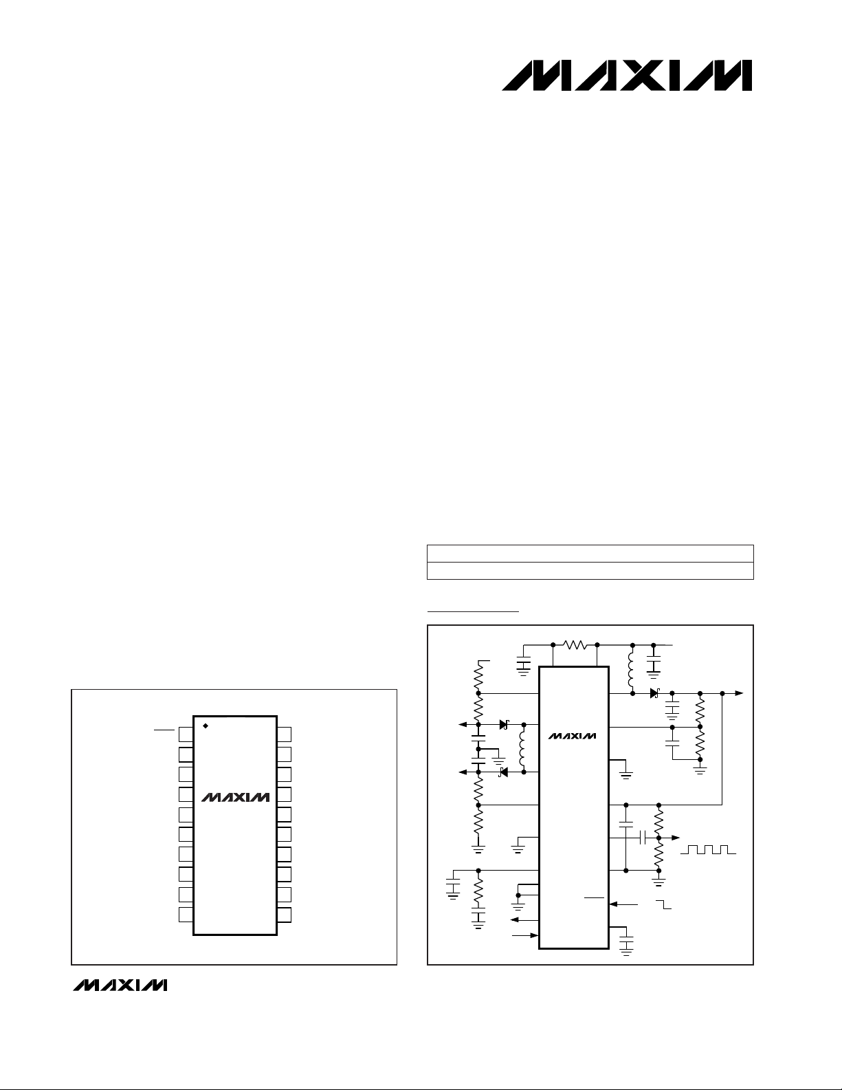
Typical Operating Circuit
___________________Pin Configuration
19-1356; Rev 0; 4/98
PART
MAX1664CUP 0°C to +70°C
TEMP. RANGE PIN-PACKAGE
20 TSSOP
_______________Ordering Information
20
19
18
17
16
15
14
13
1
2
3
4
5
6
7
8
FPLL
LX1
PGND1
PGND2REF
FB1
RDY
SHDN
TOP VIEW
LX2N
LX2P
INP
BPCLKFB2+
FB2-
IN
GND
12
11
9
10
BPV
DD
BPDRVBPV
SS
PLLC
MAX1664
TSSOP
Active-Matrix Liquid Crystal Display
(AMLCD) Supply
Page 2
MAX1664
Active-Matrix Liquid Crystal Display
(AMLCD) Supply
2 _______________________________________________________________________________________
ABSOLUTE MAXIMUM RATINGS
ELECTRICAL CHARACTERISTICS
(VIN= V
INP
= 3.3V, SHDN = IN, V
BPVDD
= 4V, V
BPVSS
= -1V, PGND1 = PGND2 = FPLL = GND, f
BPCLK
= 30kHz, TA= 0°C to +70°C,
unless otherwise noted. Typical values are at T
A
= +25°C.)
Stresses beyond those listed under “Absolute Maximum Ratings” may cause permanent damage to the device. These are stress ratings only, and functional
operation of the device at these or any other conditions beyond those indicated in the operational sections of the specifications is not implied. Exposure to
absolute maximum rating conditions for extended periods may affect device reliability.
RDY, IN, BPVDDto GND...........................................-0.3V to +6V
FB2-, PGND1, PGND2 to GND ..........................................±0.3V
LX1 to PGND1..........................................................-0.3V to +6V
BPV
SS
to GND.......................................................-3.3V to +0.3V
BPVDD to BPV
SS
......................................................-0.3V to +6V
BPDRV to BPV
SS
..................................-0.3V to (V
BPVDD
+ 0.3V)
LX2P to INP ............................................................-15V to +0.3V
LX2N to PGND2......................................................-0.3V to +30V
SHDN, INP, FB1, FB2+, REF, PLLC,
BPCLK, FPLL to GND................................-0.3V to (V
IN
+0.3V)
RDY Sink Current................................................................20mA
LX2P, LX2N Peak Switch Currents.................................±750mA
Continuous Power Dissipation (TA= +70°C)
20-Pin TSSOP (derate 7mW/°C above+70°C) ..............559mW
Operating Temperature Range...............................0°C to +70°C
Junction Temperature......................................................+150°C
Storage Temperature Range.............................-65°C to +160°C
Lead Temperature (soldering, 10sec).............................+300°C
FPLL = IN
FPLL = REF
FPLL = GND
Rising edge, 2% hysteresis
V
LX1
= 6V
FPLL = REF
FPLL = GND
V
FB1
= 1.3V
V
FB1+
= V
FB2+
= 1.3V, V
FB2-
= -0.1V;
IIN+ I
INP
SHDN = GND, VIN= 5.5V; IIN+ I
INP
FPLL = IN
CONDITIONS
8 x f
BPCLK
12 x f
BPCLK
Hz
16 x f
BPCLK
f
OP2(MAX)
Maximum Operating Frequency
V-10 0V
OUT2-
Negative Output Voltage Range
VV
IN
28V
OUT2+
Positive Output Voltage Range
V1.091 1.125 1.159V
TH_RDY
Power-Ready Trip Level
A1.2 1.5 1.8I
LIM(LX1)
LX1 Peak Current Limit
µA0.1 10I
LKG(LX1)
LX1 Leakage Current
Ω0.25 0.5R
ON(LX1)
LX1 On Resistance
nA100I
FB1
FB1 Input Bias Current
16 x f
BPCLK
Operating Frequency
V2.5 2.8V
UVLO
V2.8 5.5V
IN
Input Supply Range
Undervoltage Lockout
Threshold
24 x f
BPCLK
Hz
32 x f
BPCLK
f
OP1
VV
IN
5.5V
OUT1
Output Voltage Range
mA0.5 2I
Q
Quiescent Current
µA0.01 10I
SD
Shutdown Current
UNITSMIN TYP MAXSYMBOLPARAMETER
0 < I
LX1
< 1.2A V1.2125 1.2500 1.275V
FB1
FB1 Regulation Voltage
DC-DC 1 (PWM MAIN OUTPUT)
DC-DC 2 (PFM)
Page 3
MAX1664
Active-Matrix Liquid Crystal Display
(AMLCD) Supply
_______________________________________________________________________________________ 3
ELECTRICAL CHARACTERISTICS (continued)
(VIN= V
INP
= 3.3V, SHDN = IN, V
BPVDD
= 4V, V
BPVSS
= -1V, PGND1 = PGND2 = FPLL = GND, f
BPCLK
= 30kHz, TA= 0°C to +70°C,
unless otherwise noted. Typical values are at T
A
= +25°C.)
V
BPCLK
= 0 or 3.3V
SHDN = GND
Source and sink
Rising edge, 40mV hysteresis
SHDN = GND
Falling edge, 40mV hysteresis
V
LX2N
= 28V, V
LX2P
= -10V
V
FB2+
= 1.3V, V
FB2-
= -0.1V
CONDITIONS
µA0.01 1I
IN(BPCLK)
BPCLK Input Current
V0.7 x V
IN
V
IH(BPCLK)
BPCLK Input High Voltage
V0.3 x V
IN
V
IL(BPCLK)
BPCLK Input Low Voltage
µA80 200I
IN(BPVDD)
BPVDDSupply Current
µA-10 10I
LKG(BPDRV)
BPDRV Leakage Current
Ω0.35 0.7R
ON(BPDRV)
BPDRV On-Resistance
µA0.1 10I
SHDN(BP)
BPVDDShutdown Current
V2.5 5.5V
VDD to VSS
BPVDDto BPVSSVoltage
Range
V-3 0V
BPVSS
BPVSSSupply Range
V2.5 5.5V
BPVDD
BPVDDSupply Range
mV-15 0 15V
FB2-
V1.225 1.25 1.275V
FB2+
FB2+ Regulation Voltage
FB2- Regulation Voltage
V1.091 1.125 1.159V
TH(RDY)
FB2+ Power-Ready Trip Level
mV85 120 165V
TH(RDY)
FB2- Power-Ready Trip Level
µA0.05 10
I
LKG(LX2N)
,
I
LKG(LX2P)
LX2N, LX2P Leakage Current
nA-100 100
I
FB2+
,
I
FB2-
FB2+, FB2- Input Bias Current
Ω0.9 1.7
R
ON(LX2N)
,
R
ON(LX2P)
LX2N, LX2P On-Resistance
UNITSMIN TYP MAXSYMBOLPARAMETER
C
PLLC
= 22nF
R
PLLC
= 100kΩ
C
SHUNT
= 2.2nF
PLLC = REF, BPCLK = GND
40 72
BPCLK Input Frequency
Range
27 48 kHz
20 36
f
BPCLK
MHz1.63 1.92 2.20f
C
VCO Center Frequency
(Note 1)
-2µA < I
REF
< 50µA
V0.90 1.05 1.20V
REF(UVLO)
Undervoltage Lockout
V1.225 1.250 1.275V
REF
Reference Voltage
(0.10 x VIN) typical hysteresis V0.3 x V
IN
V
IL(SHDN)
SHDN Input Low Voltage
FPLL = GND or IN µA0.01 1I
IN(FPLL)
FPLL Input Current
µA0.01 1I
IN(SHDN)
SHDN Input Current
V0.7 x V
IN
V
IH(SHDN)
SHDN Input High Voltage
I
SINK
= 2mA V0.05 0.4V
OL(RDY)
RDY Output Low Voltage
V
RDY
= 5.5V µA0.01 1I
LKG(RDYOH)
RDY Output High Leakage
FPLL = GND
FPLL = REF
FPLL = IN
Note 1: DC-DC 1 operates at one-half of the VCOfrequency (fC / 2).
BACKPLANE DRIVER
PLL
LOGIC SIGNALS
Page 4
MAX1664
Active-Matrix Liquid Crystal Display
(AMLCD) Supply
4 _______________________________________________________________________________________
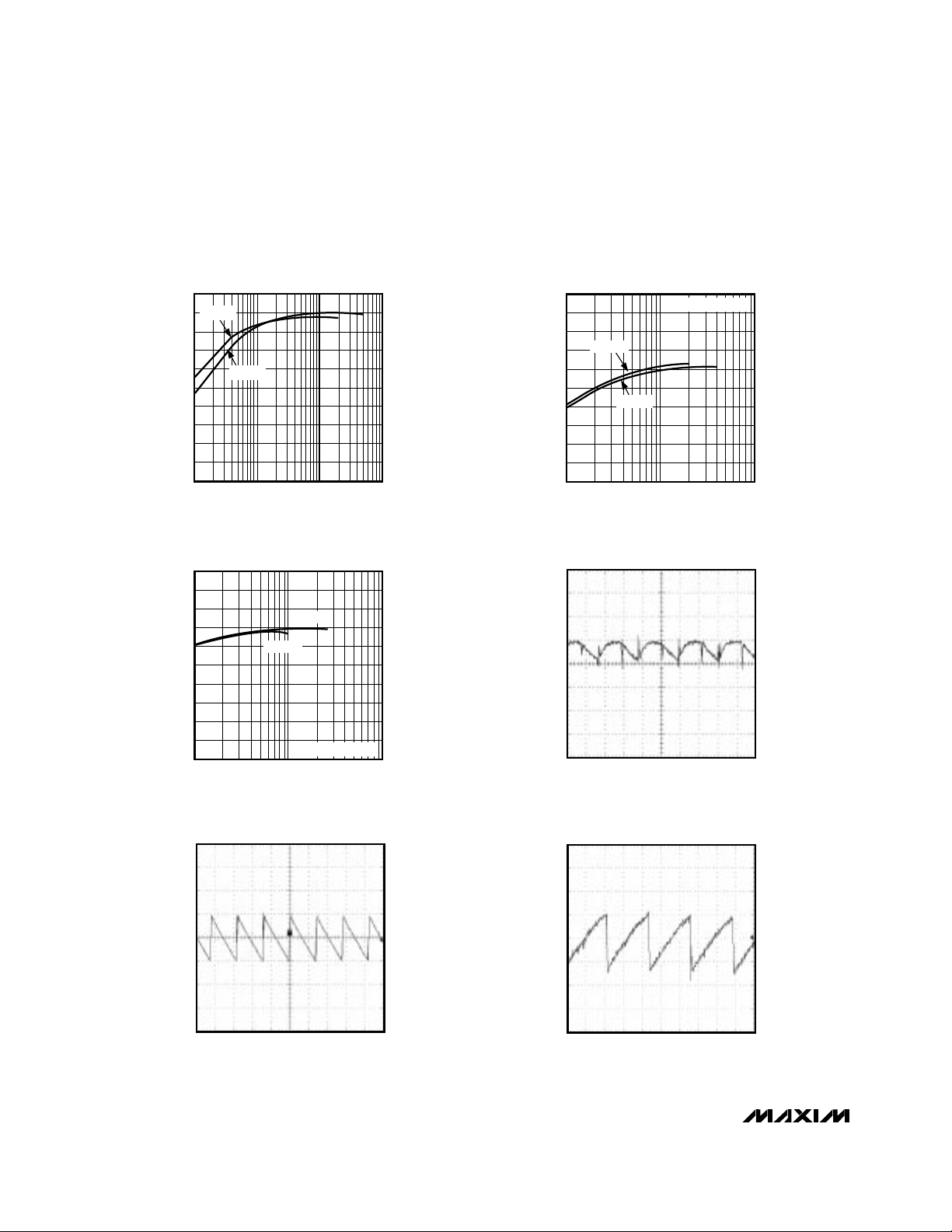
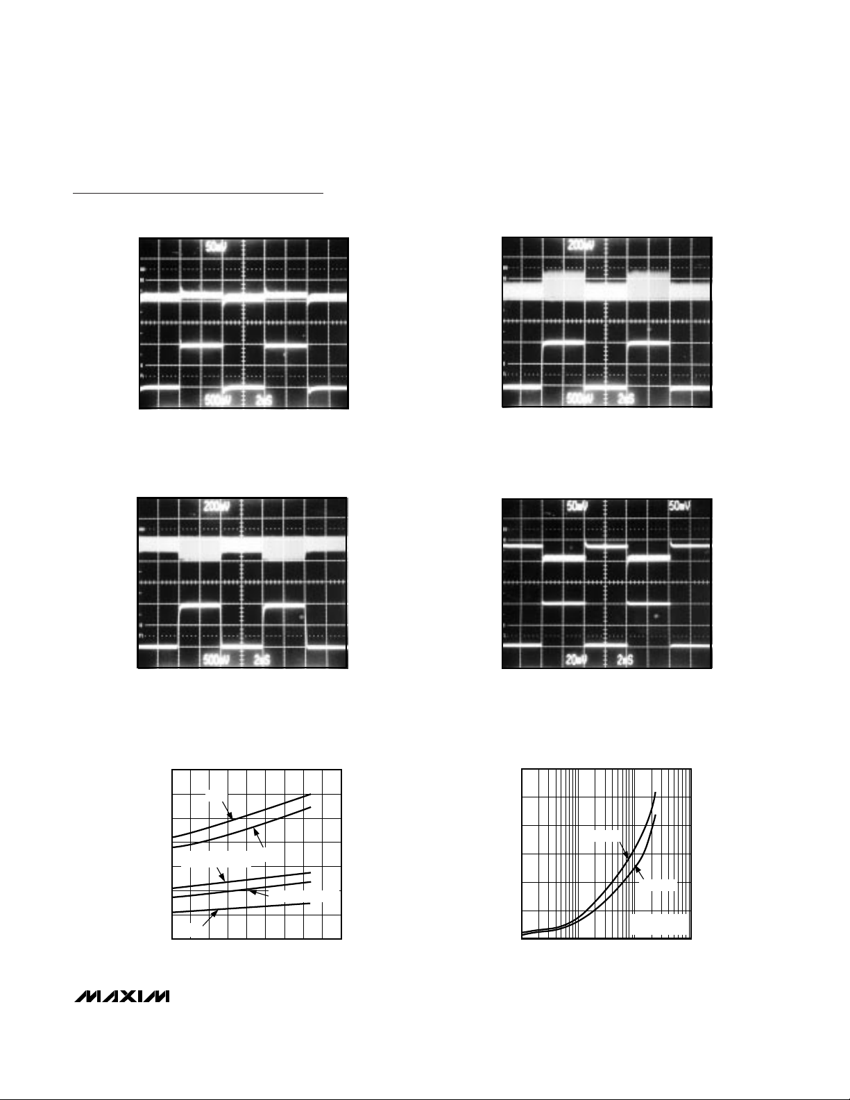
__________________________________________Typical Operating Characteristics
(f
BPCLK
= 22.5kHz, FPLL = GND, L1 = 3.3µH, L2 = 4.7µH, TA= +25°C, unless otherwise noted.)
100
0
1 10 100 1000
DC-DC 1 EFFICIENCY vs. LOAD CURRENT
(V
OUT1
= +5V)
20
MAX1664 TOC01
LOAD CURRENT (mA)
EFFICIENCY (%)
40
60
80
90
10
30
50
70
VIN = 3V
VIN = 4.5V
100
0
1 10 100
DC-DC 2 EFFICIENCY vs. LOAD CURRENT
(V
OUT2-
= -5V)
20
10
MAX1664 TOC02
LOAD CURRENT (mA)
EFFICIENCY (%)
40
30
60
70
50
80
90
V
OUT2+
UNLOADED
VIN = 5V
VIN = 3.3V
100
0
1 10 100
DC-DC 2 EFFICIENCY vs. LOAD CURRENT
(V
OUT2+
= +15V)
20
10
MAX1664 TOC03
LOAD CURRENT (mA)
EFFICIENCY (%)
40
30
60
70
50
80
90
V
OUT2-
UNLOADED
VIN = 5V
VIN = 3.3V
10mV/div
V
OUT1
RIPPLE
MAX1664 TOC04
I
OUT1
= 250mA, L = 3.3µH
500ns/div
V
OUT2
100mV/
div
V
OUT2+
RIPPLE
MAX1664 TOC05
2µs/div
V
OUT2+
= 15V, VIN = 3.3V, I
LOAD
= 9mA,
C
OUT2
= 0.22µF, AC COUPLED
V
OUT2-
50mV/
div
V
OUT2-
RIPPLE
MAX1664 TOC06
5µs/div
V
OUT2-
= -5V, VIN = 3.3V, I
LOAD
= 5mA,
C
OUT2-
= 0.47µF, AC COUPLED
Page 5
MAX1664
Active-Matrix Liquid Crystal Display
(AMLCD) Supply
_______________________________________________________________________________________
5
Typical Operating Characteristics (continued)
(f
BPCLK
= 22.5kHz, FPLL = GND, L1 = 3.3µH, L2 = 4.7µH, TA= +25°C, unless otherwise noted.)
V
OUT2-
= -5V, I
LOAD
= 5mA, C
OUT2-
= 0.47µF
A: V
OUT2-
, 200mV/div, AC COUPLED
B: V
IN
, 3V to 4V
V
OUT2-
LINE-TRANSIENT RESPONSE
A
B
MAX1664 TOC09
200mV/
div
500mV/
div
2ms/div
V
OUT1
= 5V, VIN = 3.3V, C
OUT1
= 20µF
A: V
OUT1
, 50mV/div, AC COUPLED
B: I
OUT1
, 25mA TO 225mA, 100mA/div
V
OUT1
LOAD-TRANSIENT RESPONSE
A
B
MAX1664 TOC10
50mV/
div
100mA/
div
2ms/div
0
400
200
800
600
1200
1000
1400
0 20 3010 40 50 60 70 80 90
INTERNAL FET ON-RESISTANCE
vs. TEMPERATURE
MAX1664 TOC 11
TEMPERATURE (°C)
INTERNAL FET ON-RESISTANCE (mΩ)
LX2N
LX2P
BPDRV N-CHANNEL
LX1
BPDRV P-CHANNEL
300
0
0.001 0.01 0.1 1
BPDRV RISE AND FALL TIME
vs. LOAD CAPACITANCE
MAX1664 TOC12
LOAD CAPACITANCE (µF)
RISE/FALL TIME (ns)
100
200
250
50
150
C
LOAD
FROM
BPDRV TO GND
RISE TIME
FALL TIME
V
OUT1
= 5V, I
LOAD
= 250mA, C
OUT1
= 20µF
A: V
OUT1
, 50mV/div, AC COUPLED
B: V
IN
, 3V to 4V
V
OUT1
LINE-TRANSIENT RESPONSE
A 50mV/
div
500mV/
div
2ms/div
B
MAX1664 TOC07
V
OUT2+
= 15V, I
LOAD
= 5mA, C
OUT2+
= 0.22µF
A: V
OUT2+
, 200mV/div, AC COUPLED
B: V
IN
, 3V to 4V
V
OUT2+
LINE-TRANSIENT RESPONSE
A
B
MAX1664 TOC08
200mV/
div
500mV/
div
2ms/div
Page 6

MAX1664
Active-Matrix Liquid Crystal Display
(AMLCD) Supply
6 _______________________________________________________________________________________
Typical Operating Characteristics (continued)
(f
BPCLK
= 22.5kHz, FPLL = GND, L1 = 3.3µH, L2 = 4.7µH, TA= +25°C, unless otherwise noted.)
VIN = 3.3V; V
OUT2+
= 15V/8mA, V
OUT2-
= -5V/10mA
NOTE: LX2N, LX2P PULSES ARE SYNCHED TO DC-DC 1
DC-DC 2 SWITCHING WAVEFORMS
DISCONTINUOUS CONDUCTION
VLX2N
V
LX2P
I
L2
5V/div
500mA/
div
1µs/div
5V/div
C
LOAD
= 10,000pF
BPCLK TO BPDRV FALLING DELAY
BPCLK
BPDRV
2V/div
5V/div
100ns/div
MAX1664 TOC14
5V/div
2V/div
BPDRV
BPCLK
100ns/div
BPCLK TO BPDRV RISING DELAY
MAX1664 TOC14(a))
C
LOAD
= 10,000pF
0
0.4
0.2
1.0
0.8
0.6
1.6
1.4
1.2
1.8
0 21 3 4 5 6
NO-LOAD SUPPLY CURRENT
vs. INPUT VOLTAGE
MAX1664 TOC15
INPUT VOLTAGE (V)
NO-LOAD SUPPLY CURRENT (mA)
INCLUDES ALL
EXTERNAL COMPONENT
CURRENTS
5V/div
2V/div
5V/div
5V/div
10V/div
5V/div
SHDN
V
REF
V
OUT2-
V
OUT2+
RDY
V
OUT1
500µs/div
OUT-OF-SHUTDOWN SEQUENCE
MAX1664 TOC16(a)
5V/div
500mA/div
V
LX1
I
LI
I
OUT1
= 300mA, L1 = 3.3µH
500ns/div
DC-DC 1 SWITCHING WAVEFORMS
MAX1664 TOC17(a)
Page 7

MAX1664
Active-Matrix Liquid Crystal Display
(AMLCD) Supply
_______________________________________________________________________________________ 7
PLL Compensation. Connect compensation network as in Figure 4.PLLC9
Backplane Driver Negative Supply. Typically connected to PGND1. May be connected to a separate supply.BPV
SS
10
Backplane Driver OutputBPDRV11
Backplane Driver Positive Supply. Typically connected to V
OUT1
of DC-DC 1. May be connected to a
separate supply.
BPV
DD
12
Backplane Driver Clock Input. See Table 1 for input frequency ranges.BPCLK13
Analog Ground. Connect to PGND1 and PGND2. See
Supply Connections and Layout
section.GND5
Supply Input to the IC. The input voltage range is +2.8V to +5.5V.IN6
Regulator Feedback Input for Negative Output, DC-DC 2. Regulates to 0V nominal.FB2- 7
Regulator Feedback Input for Positive Output, DC-DC 2. Regulates to 1.25V nominal.FB2+8
Internal Reference Output. Connect a 0.22µF capacitor from this pin to GND. REF can source up to 50µA.REF4
Regulator Feedback Input, DC-DC 1. Regulates to 1.25V nominal.FB13
PIN
Ready Indicator Output, DC-DC 1 and DC-DC 2. Open-drain N-channel output becomes high impedance
when all three outputs are within 10% of regulation.
RDY2
Shutdown Input. Drive low to enter shutdown mode. Drive high or connect to IN for normal operation. All IC
sections are off when SHDN is low.
SHDN
1
FUNCTIONNAME
Power Ground 1. Connect to PGND2. Source of internal LX1 N-channel MOSFET.PGND118
Drain of Internal LX1 N-Channel MOSFETLX119
Sets the BPCLK input frequency range for PLL synchronization. Connect to GND, REF, or IN. See Table 1.FPLL20
DC-DC 2 Power Input. Source of Internal LX2P P-channel MOSFET.INP14
Drain of Internal LX2P P-Channel MOSFETLX2P15
Drain of Internal LX2N N-Channel MOSFETLX2N16
Power Ground 2. Connect to PGND1. Source of internal LX2N N-channel MOSFET.PGND217
______________________________________________________________Pin Description
Page 8

MAX1664
Active-Matrix Liquid Crystal Display
(AMLCD) Supply
8 _______________________________________________________________________________________
_______________Detailed Description
The MAX1664 combines power supply and backplane
drive circuitry for active matrix thin-film-transistor (TFT)
liquid crystal displays (LCD) into one IC. Included are a
pulse-width-modulation (PWM) boost converter, a dualoutput (positive and negative) converter using one
inductor, an LCD backplane driver, and a phaselocked loop (PLL) to synchronize all three outputs to the
backplane clock.
A high switching frequency (1MHz nominal) and phaselocked operation allow the use of small, minimumheight external components while maintaining low
output noise. Output voltages are adjustable to +5.5V
(DC-DC 1) and to +28V and -10V (DC-DC 2). The negative output voltage can be set to as low as -20V with
additional components.
The frequency ratio between the DC-DC 1 converter
and the backplane clock can be set to 16, 24, or 32.
This flexibility allows high DC-DC converter frequencies
to be used with LCD backplane clock rates ranging
from 20kHz to 72kHz.
Start-Up
At start-up, both converters remain disabled until V
REF
reaches 90% of its nominal value. V
OUT1
is activated
first. Once V
OUT1
is regulated, V
OUT2-
is enabled.
V
OUT2+
is held at 0 until V
OUT2-
is within 90% of its regulation target. All three outputs power up in a similar
order when power is applied or when coming out of
shutdown. See the Out-of-Shutdown Sequence photo in
the
Typical Operating Characteristics
section.
DC-DC 1 Boost Converter
DC-DC 1 uses a current-mode boost PWM architecture
to produce a positive regulated voltage, adjustable
from 3V to 5.5V (but not less than VIN). This converter
uses an internal N-channel MOSFET with a maximum
on-resistance of 0.5Ω. Cycle-by-cycle peak current limiting protects the switch under fault conditions. Upon
start-up, DC-DC 1 is the first converter to be enabled.
BACKPLANE
DRIVER
BPV
SS
BPDRV
BPV
DD
PGND1
FB1
LX1
V
SUPPLY
2.8V TO 5.5V
V
OUT1
5.5V
SHDN
REF
1.25V
REF
PHASE
DET
VCO
÷4 ÷2
÷N
FPLL
BPCLK
PLLC
PGND2
FB2+
LX2N
DC-DC 2 DC-DC 1
LX2P
INP IN
FB2-
REF
V
OUT2-
-10V
V
OUT2+
28V
IN
REF
GND
GNDRDY
MAX1664
Figure 1. Functional Diagram
Page 9

MAX1664
Active-Matrix Liquid Crystal Display
(AMLCD) Supply
_______________________________________________________________________________________ 9
Fixed-frequency, current-mode operation ensures that
the switching noise exists only at the operating frequency and its harmonics. The switching frequency is phase
locked to the backplane clock input. Table 1 illustrates
the possible switching-frequency options.
DC-DC 2 Dual Outputs
DC-DC 2 uses a synchronized, fixed on-time PFM
architecture to provide the positive and negative output
voltages that allow the driver ICs to turn the TFT gates
on and off. When pulses occur, they are synchronized
to DC-DC 1, thereby minimizing converter interactions
and subharmonic interference.
The DC-DC 2 inductor current is always discontinuous,
enabling the dual outputs to be regulated independently. This allows one output to be at 100% load while the
other is at no load.
DC-DC 2 Operation
In normal operation, DC-DC 2 alternates between
charging the negative and positive outputs (Figure 1).
During the first half-cycle of the PFM clock period, both
the N-channel and P-channel MOSFETs turn on, applying the input supply across inductor L2. This causes
the inductor current to ramp up at a rate proportional to
V
INP
. During the second half-cycle, the P-channel
MOSFET turns off and the inductor transfers its energy
into the negative output filter capacitor.
Assuming that the energy transfer is completed during
this second half-cycle and the inductor current ramps
down to zero, the process is repeated for the positive
output during the next clock cycle. During the first half
of the second clock cycle, both the N-channel and Pchannel MOSFETs turn on again. The current in the
inductor again rises at the same rate. During the second half of the second clock cycle, the N-channel
MOSFET is turned off and this time the inductor energy
transfers to the positive output filter capacitor.
During conditions of heavy loads, DC-DC 2 will continue to operate in this manner, alternately delivering
pulses to the negative and positive outputs. For lighter
loads, the controller may skip one or more cycles of
either polarity, thereby keeping the outputs in regulation. See Table 1 for the relationship between the maximum DC-DC 2 pulse frequency and the backplane
clock frequency.
Outputs with Low Step-Up or Inversion Ratios
For DC-DC 2 output voltage setpoints, which require
minimum step-up or inversion ratios (for example,
V
OUT+
< 6V or V
OUT-
> -3V, when V
INP
= 5V), more
than one half-cycle may be required to transfer the
inductor energy to the appropriate output filter capacitor. In such cases, subsequent conversion cycles are
delayed, as necessary, by one or more PFM clock
cycles to preserve discontinuous mode operation.
Backplane Driver
The MAX1664 provides a low-impedance backplane driver, as shown in Figure 1, that level-translates the BPCLK
signal from a logic level to BPVDD/BPVSSlevels. The
backplane driver consists of an N-channel/P-channel
complementary pair of high-current MOSFETs. These
devices drive BPDRV to either BPVDDor BPV
SS
when
BPCLK goes either high or low, respectively. The switches have a maximum on-resistance of 0.7Ω with a typical
propagation delay of 50ns. Power for the backplane driver can be taken from the output of DC-DC 1, V
OUT1
, as
shown in the
Typical Operating Circuit
.
Phase-Locked Loop
The MAX1664 contains an on-board PLL to synchronize
the PWM and PFM converter clocks to the backplane
clock (Figure 2). This will minimize noise and interference. The PLL is a frequency-multiplying type, generating a nominal 1MHz clock signal for DC-DC 1 and a
nominal 500kHz clock for DC-DC 2. Three input frequency ranges, spanning 20kHz to 72kHz, permit synchronization over a broad range of backplane clock
input frequencies while maintaining optimal conversion
frequencies (Table 1).
FPLL
f
BPCLK
(kHz)
f
DC-DC 1
(kHz)
f
DC-DC 2 MAX
(kHz)
f
DC-DC 1
:
f
BPCLK
f
DC-DC 2 MAX
:
f
BPCLK
N*
IN 40 to 72 640 to 1152 320 to 576 16:1 8:1 32
REF 27 to 48 640 to 1152 320 to 576 24:1 12:1 48
GND 20 to 36 640 to 1152 320 to 576 32:1 16:1 64
Table 1. Switching Frequency Options
*
See Figure 2
Page 10

MAX1664
Active-Matrix Liquid Crystal Display
(AMLCD) Supply
10 ______________________________________________________________________________________
The heart of the PLL is the VCO, which is trimmed to a
nominal frequency of 1.92MHz for a control voltage (at
the PLLC pin) of 1.250V. This high-frequency internal
clock is divided digitally with a division ratio selected
by pin-strapping FPLL to GND, REF, or IN. This divided
clock is compared to the backplane clock by an internal phase comparator (rising-edge triggered). The
phase detector in turn adjusts the VCO control voltage
until the two frequencies (and phases) match. This
feedback loop is compensated at the PLLC pin.
In some applications, the backplane clock may be halted for several cycles between screen scans or may not
be immediately applied on power-up. The PLL contains
a proprietary phase-detector architecture that minimizes frequency error during clock dropouts of more
than two cycles and re-establishes lock immediately
when the clock resumes.
Ready Indicator (RDY)
The RDY pin has an open-drain output and indicates
when all three outputs are in regulation. The open-drain
output becomes high impedance when all three converter outputs are within 10% of their regulation setpoints.
Design Procedure and
______________Component Selection
Output Voltage Selection
The three output voltages as well as the DC bias for the
backplane clock are adjustable on the MAX1664, as
shown in Figure 3. Set each output using two standard
1% resistors to form a voltage divider between the
selected output and its respective feedback pin. Use
the following equations to calculate the resistances.
DC-DC 1 Output
For V
OUT1
= 5V, typical values are R2 = 100kΩ and R1
= 301kΩ. To set V
OUT1
to another voltage, choose R2 =
100kΩ and C
FB1
= 50pF, and calculate R1 as follows:
DC-DC 2 Positive Output
For V
OUT2+
= 15V, typical values are R8 = 49.9kΩ and
R7 = 549kΩ. To set V
OUT2+
to another voltage, choose
R8 = 49.9kΩ and calculate R7 as follows:
DC-DC 2 Negative Output
For the negative output voltage, the FB2- threshold voltage is 0. For V
OUT2-
= -5V, typical values are R5 =
49.9kΩ and R6 = 200kΩ. To set V
OUT2+
to another volt-
age, choose R5 = 49.9kΩ and calculate R6 as follows:
DC Bias for the Backplane Driver
For V
DCBIAS
= V
BPVDD
/2, typical values are R3 = R4 =
100kΩ. To set the DC bias to a different value, choose
R4 and calculate R3 as follows:
R3 R4
V - V
V - V
- 1
BPVDD BPVSS
DCBIAS BPVSS
=
R6 R5
V
V
OUT2-
REF
=
R7 R8
V
V
- 1
OUT2
FB2
=
+
+
R1 R2
V
V
- 1
OUT1
FB1
=
PHASE
DETECTOR
VCO
÷4
÷2
PLLC
÷N*
IN
REF
BPCLK
*SEE TABLE 1 FOR
SELECTED VALUES OF N.
DC-DC 1
R
PLLC
C
PLLC
C
SHUNT
DC-DC 2
GND
Figure 2. Internal PLL Operation within the MAX1664
BPV
DD
C
FB1
R2
R1
FB2+
FB2-
BPDRV
FB1
R5
R6
V
OUT2-
R7
R8
REF
BPV
SS
C
C
V
OUT1
V
OUT2+
R3
DC
BIAS
R4
MAX1664
Figure 3. Output Voltage Selection
Page 11

MAX1664
Active-Matrix Liquid Crystal Display
(AMLCD) Supply
______________________________________________________________________________________ 11
Inductor Selection
The optimum inductor value for L1 is 3.3µH, as shown
in Figure 4. Inductors with less than 300mΩ DC series
resistance are recommended to achieve the highest
efficiency. Using a larger value for L1 (e.g., 4.7µH)
increases the output current capability of DC-DC 1 (by
reducing the peak ripple current) at the expense of size
and the additional output filter capacitance needed for
loop stability.
For DC-DC 2, at large input voltages (i.e., 5V) and low
switching frequencies (i.e., ≤400kHz), the value of L2
should be increased (e.g., 6.8µH or 10µH) to limit the
peak current. In some cases it may be necessary to
reduce the value of L2 to increase the output current
capability of DC-DC 2 (Table 2). The relationship between
input voltage, output voltage, switching frequency, inductor value, and maximum load current for DC-DC 2 is complex and nonlinear. This relationship is summarized in
Table 2. The L2 equation is as follows:
where:
Internal MOSFET on-resistance:
R
ON(LX2P)
= R
ON(LX2N)
= 0.9Ω typical
External inductor DC resistance:
R
L2
= 0.3Ω typical
Inductor peak current:
I
PEAK
= 700mA (750mA absolute maximum)
Due to the MAX1664’s high switching frequency, inductors with a high-frequency core material such as ferrite
are recommended. Powdered iron compounds are not
recommended due to their higher core losses. Typical
small-size, low-profile inductors include the ILS-3825
(Dale Electronics-Vishay) and the CLQ61B (Sumida).
These inductors are primarily used for DC-DC
converters with low height requirements. See Table 3
for more information on manufacturers who provide
low-profile inductors.
L2
V - R R R
(I )
2
I x 2 f
INP ON(LX2P) ON(LX2N) L2
PEAK
PEAK DC-DC 1
>
+ +
[ ]
( )
REF
FB2-
IN INP
LX2P
LX2N
FB2+
R8
49.9k
R7
549k
R6
200k
R5
49.9k
D3
D2
L2
4.7µH
PGND2
PLLC
GND
FPLL
RDY
REF
SHDN
ON
OFF
V
OUT1
5.5V
2.2µF
3 x 10µF
0.22µF
22nF
100k
2.2nF
0.22µF
0.47µF
50pF
2 x 10µF
10µF
10µF2.2µF
33Ω
0.47µF
3.3µH
R1
301k
R2
100k
R3
100k
R4
100k
V
OUT2-
-5V
V
OUT2+
15V
BPV
SS
BACKPLANE
DRIVER
V
SUPPLY
2.8V TO 5.5V
BPDRV
BPV
DD
PGND1
FB1
LX1
BPCLK
MAX1664
Figure 4. Detailed Typical Operating Circuit
Page 12

MAX1664
12 ______________________________________________________________________________________
Diode Selection
The MAX1664’s high switching frequency requires fast
diodes. Schottky diodes such as the MBR0520L and
MBR0540L (Motorola) are recommended because they
have the necessary power ratings in a low-height SOD123 package. Also recommended is the MBRM5817
which is 1.1mm high. Use a Schottky diode with a forward current rating greater than:
For the positive output of DC-DC 2, use a Schottky
diode with a voltage rating that exceeds V
OUT2+
. For
the negative output, use a Schottky diode with a rating
that exceeds V
IN
+ V
OUT2-
. See Table 3 for more
information on Schottky diode manufacturers.
Filter Capacitor Selection
An output filter capacitor’s ESR and size can greatly
influence a switching converter’s output ripple, as
shown in the following equation.
V I x R I
t
C
DC-DC 1 t
1
f
V V - V
V V
DC-DC 2 t
1
2 f
RIPPLE(PK PK) PEAK ESR OUT
ON
OUT
ON
DC-DC 1
OUT1 F IN
OUT1 F
ON
DC-DC 1
−
≅ +
=
+
+
=
.
I
I V
V
F
OUT OUT
IN
>
0 9
Table 2. Typical DC-DC 2 Operation
*
Note: Absolute maximum peak current at LX2P and LX2N is 750mA.
Active Matrix Liquid Crystal Display
(AMLCD) Supply
INDUCTOR PEAK
CURRENT*
(mA)
f
DC-DC 2(MAX)
(kHz)
I
OUT2-(MAX)
(mA)
I
OUT2+(MAX)
(mA)
L2
(µH)
f
BPCLK
(kHz)
V
IN
(V)
V
OUT2-
(V)
V
OUT2+
(V)
50048015104.730.05.0-10+20
55040018104.725.05.0-10+20
64036020114.722.55.0-10+20
67948017102.730.04.5-10+20
4504801284.730.04.5-10+20
5004001484.725.04.5-10+20
5803601694.722.54.5-10+20
496480844.730.03.3-10+20
340480544.730.03.3-10+20
5834001062.725.03.3-10+20
370400744.725.03.3-10+20
6433601262.722.53.3-10+20
425360844.722.53.3-10+20
451480632.730.03.0-10+20
300480434.730.03.0-10+20
530400842.725.03.0-10+20
340400524.725.03.0-10+20
5853601052.722.53.0-10+20
385360634.722.53.0-10+20
60036043204.722.55.0-5+15
55036035154.722.54.5-5+15
64336027102.722.53.3-5+15
4253601974.722.53.3-5+15
5853602382.722.53.0-5+15
3753601564.722.53.0-5+15
Page 13

Ceramic capacitors are recommended because they
have low ESR and the lowest profile. Typical ceramic
capacitors are the C3225X5R series from TDK and
JMK325 series from Taiyo Yuden. See Table 3 for more
information on the manufacturers who provide surfacemount ceramic capacitors.
PLL Compensation
In most applications, the recommended compensation
component values shown in Figure 4 will give optimal
system performance. If no backplane clock is used,
connect PLLC to REF.
_____________Applications Information
Increasing V
OUT
Above 5.5V
For V
OUT1
output voltages above 5.5V, connect the
supplemental charge pump circuit shown in Figure 5.
The connection shown supplies a 10V 150mA output,
but other voltages from 2 x VINto 10V can be set by
selecting the appropriate values for R1 and R2 (see
DC-DC 1 Output
section). C2–C4 are shown as parallel
combinations of 3.3µF ceramic capacitors so that a
1.1mm height restriction can be met. If height is not
restricted, then larger values can be used instead of
parallel capacitor combinations.
3.3V to -20V Charge-Pump Configuration
For applications requiring negative voltages down to
-20V, an inverting charge-pump block can be added to
the V
OUT2-
output (Figure 6). Typical values for CFand
C
OUT
are 0.47µF to 1µF and 4.7µF to 10µF, respective-
ly. As a general rule, C
OUT
should be ten times greater
than CF. This circuit operates as follows:
1) During the first PFM cycle, the voltage at V1 is
charged by inductor L2 to some fraction of its final
steady-state voltage, in the normal manner described
in the
Detailed Description
.
2) During the first half of subsequent PFM cycles, pin
LX2P is pulled to V
INP
, and capacitor CFis charged
to (V
INP
+V1 - VD), where VDis a diode forward
voltage.
3) During subsequent second half-cycles when LX2P
flies negatively below V1, capacitor CFtransfers
some of its energy to output capacitor C
OUT
, which
then is charged to a negative voltage of approximately (V
INP
+ 2 x V1 - 2x VD).
4) This process continues until V
OUT
reaches the
desired voltage, as determined by the ratio of the
FB2- feedback resistors.
5) During steady-state (in-regulation) operation, the
magnitude of the voltage at LX2P is equal to
(V
OUT
/ 2 - V
INP
/ 2 + VD), which must be limited to
less than 10V.
MAX1664
Active-Matrix Liquid Crystal Display
(AMLCD) Supply
______________________________________________________________________________________ 13
MANUFACTURER PHONE FAX
Dale Inductors (605) 668-4131 (605) 665-1627
Sumida USA (847) 956-0666 (847) 956-0702
Central Semiconductor (516) 435-1110 (516) 435-1824
International Rectifier (310) 322-3331 (310) 322-3232
TDK (847) 390-4373 (847) 390-4428
Vishay/Vitramon (203) 268-6261 (203) 452-5670
Table 3. Component Manufacturers
MAX1664
LX1
C3
3.3µF (x6)
C4
3.3µF (x2)
R2
13k
D1, D2, D3— MBRM5817
C1, C2, C3—ALL CERAMIC TYPES
R1
91k
C2
3.3µF (x2)
50pF
D2
33Ω
IN INP
D3
D1
V
1
10V
150mA
V
SUPPLY
2.8V TO 3.6V
PGND1
FB1
C1
3.3µF (x2)
3.3µH
0.47µF
Figure 5. Charge Pump Configuration to Increase V
OUT1
Above 5.5V.
Motorola (602) 303-5454 (602) 994-6430
Marcon/United
Chemicon
(847) 696-2000 (847) 696-9278
Taiyo Yuden (408) 573-4150 (408) 573-4159
INDUCTORS
DIODES
CERAMIC CAPACITORS
Page 14

MAX1664
Active-Matrix Liquid Crystal Display
(AMLCD) Supply
14 ______________________________________________________________________________________
Figure 7a. MAX1664 Component Placement Guide Figure 7b. MAX1664 PC Board Layout—Component Side
1.0"
1.0"
Supply Connections and Layout
The MAX1664 performs both precision analog and
high-power switching functions. Carefully plan supply
connections, bypassing, and layout. Bypass IN and INP
with a 33Ω isolation resistor (R9, Figure 4) between
them. In addition, sufficient low-ESR bypassing must be
provided on the INP bus to ensure stability of DC-DC 1.
A solid ground plane under the power components,
with a separate ground plane under the analog nodes,
is highly recommended. These ground planes should
be connected at a single, quiet point. Analog reference
and feedback signals should be referred to and routed
over the analog ground plane. Figure 7 shows a typical
layout using separate ground planes.
REF
R5
R6
R7
R8
FB2-
LX2P
L2
LX2N
FB2+
D3
D2
D5
D4
C
F
V1
PGND2
0.47µF
0.22µF
C
OUT
4.7µF
V
OUT2-
-20V
V
OUT2+
28V
MAX1664
Figure 6. V
OUT2
- Voltage-Doubler Charge Pump
Page 15

MAX1664
Active-Matrix Liquid Crystal Display
(AMLCD) Supply
______________________________________________________________________________________ 15
Figure 7c. MAX1664 PC Board Layout—Solder Side
TRANSISTOR COUNT: 838
___________________Chip Information
1.0"
Page 16

MAX1664
Active-Matrix Liquid Crystal Display
(AMLCD) Supply
Maxim cannot assume responsibility for use of any circuitry other than circuitry entirely embodied in a Maxim product. No circuit patent licenses are
implied. Maxim reserves the right to change the circuitry and specifications without notice at any time.
16
____________________Maxim Integrated Products, 120 San Gabriel Drive, Sunnyvale, CA 94086 408-737-7600
© 1998 Maxim Integrated Products Printed USA is a registered trademark of Maxim Integrated Products.
________________________________________________________Package Information
TSSOP.EPS
 Loading...