

Page 1
_______________General Description
The MAX1642/MAX1643 are high-efficiency, low-voltage,
step-up DC-DC converters intended for devices powered by a single alkaline cell. They feature low quiescent supply currents and are supplied in the ultra-small
µMAX package, which is only 1.1mm high. The guaranteed start-up voltage is 0.88V.
Each device consists of an internal 1Ω, N-channel
MOSFET power switch; a built-in synchronous rectifier
that acts as the catch diode; an oscillator; a reference;
and pulse-frequency-modulation (PFM) control circuitry.
Both devices feature an independent undervoltage
comparator (PFI/PFO). The MAX1642 also includes a
2µA logic-controlled shutdown mode. The MAX1643
offers a dedicated low-battery detector (BATTLO) in
lieu of shutdown.
The output voltage for each device is preset to 3.3V
±4%, or can be adjusted from +2V to +5.2V using only
two resistors.
________________________Applications
Pagers
Remote Controls
Pointing Devices
Personal Medical Monitors
Single-Cell Battery-Powered Devices
____________________________Features
♦ Built-In Synchronous Rectifier
♦ 0.88V Guaranteed Start-Up
♦ Ultra-Small µMAX Package: 1.1mm High
♦ 83% Efficiency
♦ 4µA Quiescent Supply Current into BATT Pin
♦ 2µA Logic-Controlled Shutdown (MAX1642)
♦ Two Undervoltage Detectors (MAX1643)
♦ 2V to 5.2V Output Range
♦ 20mA Output Current at 1.2V Input
♦ Reverse Battery Protection
MAX1642/MAX1643
High-Efficiency, Step-Up
DC-DC Converters for 1V Inputs
________________________________________________________________
Maxim Integrated Products
1
GND
PFO
FB
SHDN
1
2
8
7
OUT
LX
PFI
BATT
MAX1642
µMAX
TOP VIEW
3
4
6
5
GND
BATTLO
FB
PFO
1
2
8
7
OUT
LX
PFI
BATT
MAX1643
µMAX
3
4
6
5
_________________Pin Configurations
OUT
OUTPUT
3.3V
INPUT
0.88V TO 1.65V
100µH
22µF
22µF
ON
LOW-BATTERY
DETECTOR INPUT
LOW-BATTERY
DETECTOR OUTPUT
OFF
PFO
BATT
LX
MAX1642
SHDN
PFI
GND FB
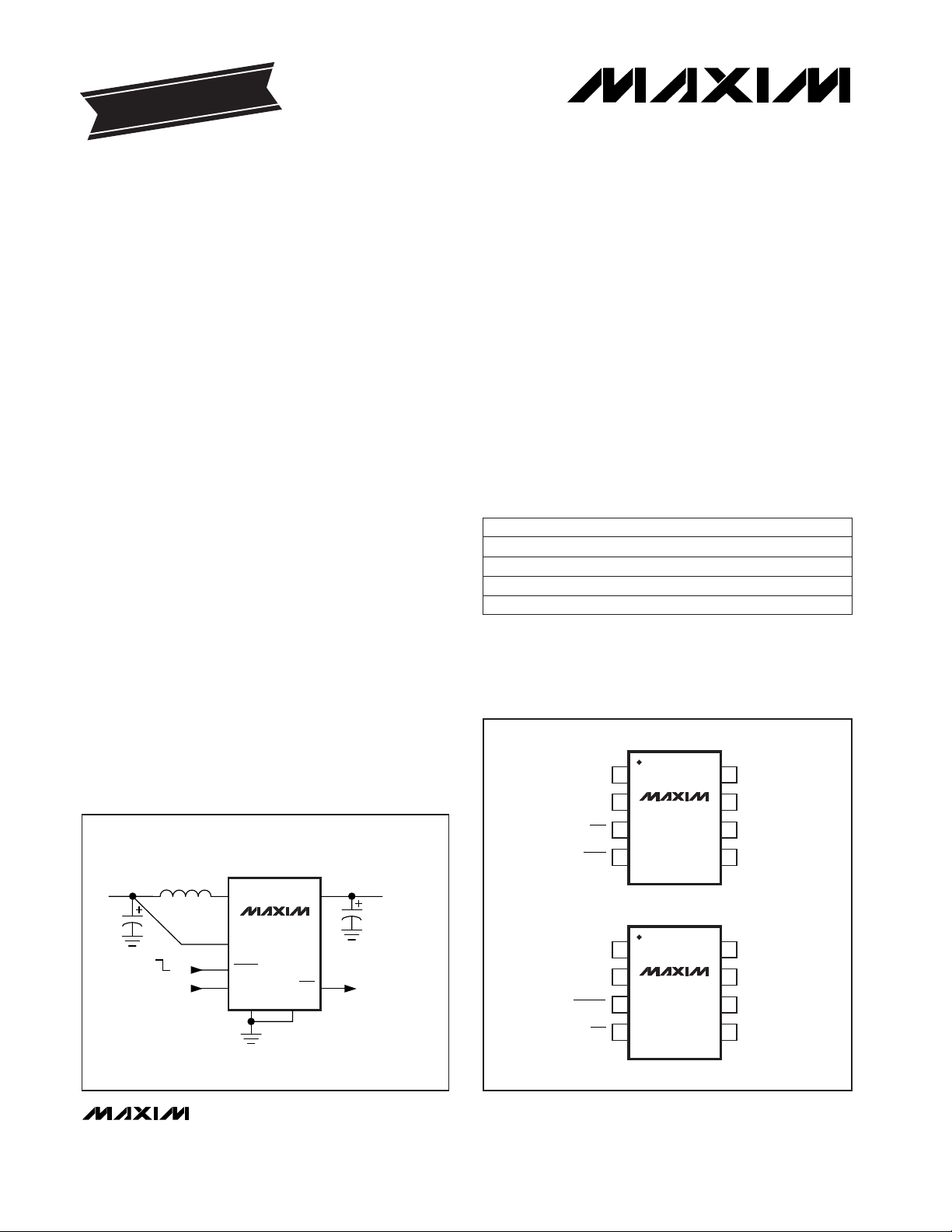
__________Typical Operating Circuit
______________Ordering Information
PART
MAX1642C/D
MAX1642EUA
MAX1643C/D
0°C to +70°C
-40°C to +85°C
0°C to +70°C
TEMP. RANGE PIN-PACKAGE
Dice*
8 µMAX
Dice*
MAX1643EUA -40°C to +85°C 8 µMAX
EVALUATION KIT MANUAL
FOLLOWS DATA SHEET
19-1183; Rev 0; 6/97
*
Dice are tested at TA= +25°C.
Note: To order these devices shipped in tape and reel, add a -T
to the part number.
For free samples & the latest literature: http://www.maxim-ic.com, or phone 1-800-998-8800.
For small orders, phone 408-737-7600 ext. 3468.
Page 2
MAX1642/MAX1643
High-Efficiency, Step-Up
DC-DC Converters for 1V Inputs
2 _______________________________________________________________________________________
ABSOLUTE MAXIMUM RATINGS
BATT to GND...........................................................-0.3V to 6.0V
BATT Forward Current..........................................................0.5A
OUT to GND.............................................................-0.3V to 6.0V
OUT, LX Current.......................................................................1A
LX to GND................................................................-0.3V to 6.0V
SHDN, FB, BATTLO, PFO to GND...........................-0.3V to 6.0V
PFI to GND............................................................-0.3V to V
BATT
Reverse Battery Current (TA= +25°C) (Note 1) ...............220mA
Continuous Power Dissipation
µMAX (derate 4.1mW/°C above 70°C)..........................330mW
Operating Temperature Range
MAX1642EUA/MAX1643EUA ............................-40°C to +85°C
Junction Temperature......................................................+150°C
Storage Temperature Range.............................-65°C to +165°C
Lead Temperature (soldering, 10sec).............................+300°C
RL= 3kΩ, TA= +25°C
VFB= 1.3V
I
LOAD
= 20mA
V
BATT
= 1.0V (MAX1642)
0.9V < V
BATT
< 1.5V (tON= K / V
BATT
)
V
OUT
= 3.5V (MAX1642)
I
DIODE
= 100mA, P-channel switch off
V
OUT
= 3.3V
VFB< 0.1V
External feedback
External feedback
V
OUT
= 3.5V
V
OUT
= 3.3V
0.9V < V
BATT
< 1.5V, V
OUT
= 3.3V
CONDITIONS
nA10FB Input Current
%80
η
Efficiency
µA2 3.5I
SHDN,BATT
Shutdown Current into BATT
µA0.1 1I
SHDN,OUT
Shutdown Current into OUT
µA4 6.5I
QBATT
Quiescent Current into BATT
µA11 18I
QOUT
Quiescent Current into OUT
1 1.5RATIOOff-Time Tracking Ratio (Note 3)
mV/°C-2Start-Up Voltage Tempco
V0.88
V0.7V
BATT(MIN)
Minimum Operating Input Voltage
Start-Up Voltage (Note 2)
V-µs17 25 35KOn-Time Constant
V0.8P-Channel Catch-Diode Voltage
Ω1.5 2.2P-Channel On-Resistance
V3.16 3.30 3.44V
OUT
Output Voltage
V2.0 5.2Output Voltage Range
V1.18 1.225 1.27V
FB
FB Set Voltage
Ω1 1.5N-Channel On-Resistance
UNITSMIN TYP MAXSYMBOLPARAMETER
ELECTRICAL CHARACTERISTICS
(V
BATT
= V
SHDN
= 1.3V, I
LOAD
= 0mA, FB = GND, TA= 0°C to +85°C, unless otherwise noted. Typical values are at TA= +25°C.)
Note 1: The reverse battery current is measured from the
Typical Operating Circuit’s
input terminal to GND when the battery is connected backward. A reverse current of 220mA will not exceed package dissipation limits but, if left for an extended time
(more than 10 minutes), may degrade performance.
Stresses beyond those listed under “Absolute Maximum Ratings” may cause permanent damage to the device. These are stress ratings only, and functional
operation of the device at these or any other conditions beyond those indicated in the operational sections of the specifications is not implied. Exposure to
absolute maximum rating conditions for extended periods may affect device reliability.
V1.65Maximum Operating Input Voltage
Falling PFI, hysteresis = 1% mV590 614 632PFI Trip Voltage
V
PFI
= 0V, V
OUT
= 3.3V, I
SINK
= 1mA
V
PFI
= 650mV
V0.4V
OL
PFO, BATTLO Low Output Voltage
nA10PFI Input Current
V
OUT
= 3.3V, hysteresis = 2% (MAX1643)
V
PFI
= 650mV, V
PFO
= 6V
V0.96 1.0 1.04
BATTLO Trip Voltage
µA1
PFO, BATTLO Leakage Current
% of V
BATT
(MAX1642)
% of V
BATT
(MAX1642)
%80V
IH
SHDN Input High Voltage
%20V
IL
SHDN Input Low Voltage
(MAX1642) nA10
SHDN Input Current
Page 3
MAX1642/MAX1643
High-Efficiency, Step-Up
DC-DC Converters for 1V Inputs
_______________________________________________________________________________________ 3
Note 2: Start-up guaranteed by correlation to measurements of device parameters (i.e., switch on-resistance, on-times, off-times, and
output voltage trip points).
Note 3: . This guarantees discontinuous conduction.
Note 4: Specifications to -40°C are guaranteed by design, not production tested.
t =
t x V
V - V
x RATIO
OFF
ON BATT
OUT BATT
Falling PFI, hysteresis = 1%
V
BATT
= 1.0V (MAX1642)
0.9V < V
BATT
< 1.5V (tON= K / V
BATT
)
V
OUT
= 3.5V (MAX1642)
V
OUT
= 3.3V
VFB< 0.1V
External feedback
V
OUT
= 3.5V
V
OUT
= 3.3V
CONDITIONS
mV 550 662PFI Trip Voltage
µA3.5I
SHDN,BATT
Shutdown Current into BATT
µA1I
SHDN,OUT
Shutdown Current into OUT
µA6.5I
QBATT
Quiescent Current into BATT
µA18I
QOUT
Quiescent Current into OUT
V-µs12.4 38.2KOn-Time Constant
Ω2.2P-Channel On-Resistance
V2.99 3.56V
OUT
Output Voltage
V1.11 1.32V
FB
FB Set Voltage
Ω1.5N-Channel On-Resistance
UNITSMIN MAXSYMBOLPARAMETER
ELECTRICAL CHARACTERISTICS
(V
BATT
= V
SHDN
= 1.3V, I
LOAD
= 0mA, FB = GND, TA= -40°C to +85°C, unless otherwise noted.) (Note 4)
Falling V
BATT
, V
OUT
= 3.3V, hysteresis = 2%
(MAX1643)
V0.93 1.06
BATTLO Trip Voltage
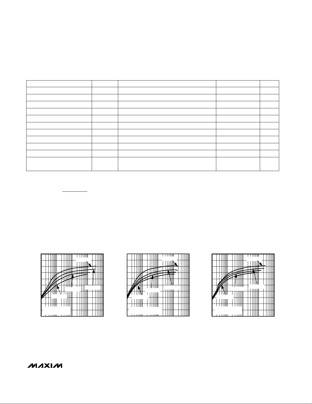
__________________________________________Typical Operating Characteristics
(Circuit of Figure 4, V
BATT
= 1.2V, R1 + R2 = 1MΩ, TA = +25°C, unless otherwise noted.)
0
0.01 1 100.1 100
EFFICIENCY vs. OUTPUT CURRENT
(V
OUT
= 2.4V)
10
MAX1642/43 TOC01A
OUTPUT CURRENT (mA)
EFFICIENCY (%)
VIN = 1.6V
L1 = 100µH
SUMIDA CD54-101
VIN = 1.2V
VIN = 0.85V
VIN = 1.0V
20
30
40
50
60
70
80
90
100
0
0.01 1 100.1 100
EFFICIENCY vs. OUTPUT CURRENT
(V
OUT
= 2.4V)
10
MAX1642/43 TOC01B
OUTPUT CURRENT (mA)
EFFICIENCY (%)
VIN = 1.6V
L1 = 150µH
TDK NLC565050T-151K
VIN = 1.2V
VIN = 0.85V
VIN = 1.0V
20
30
40
50
60
70
80
90
100
0
0.01 1 100.1 100
EFFICIENCY vs. OUTPUT CURRENT
(V
OUT
= 3.3V)
10
MAX1642/43 TOC02A
OUTPUT CURRENT (mA)
EFFICIENCY (%)
VIN = 1.6V
L1 = 100µH
SUMIDA CD54-101
VIN = 1.2V
VIN = 0.85V
VIN = 1.0V
20
30
40
50
60
70
80
90
100
Page 4
MAX1642/MAX1643
High-Efficiency, Step-Up
DC-DC Converters for 1V Inputs
4 _______________________________________________________________________________________
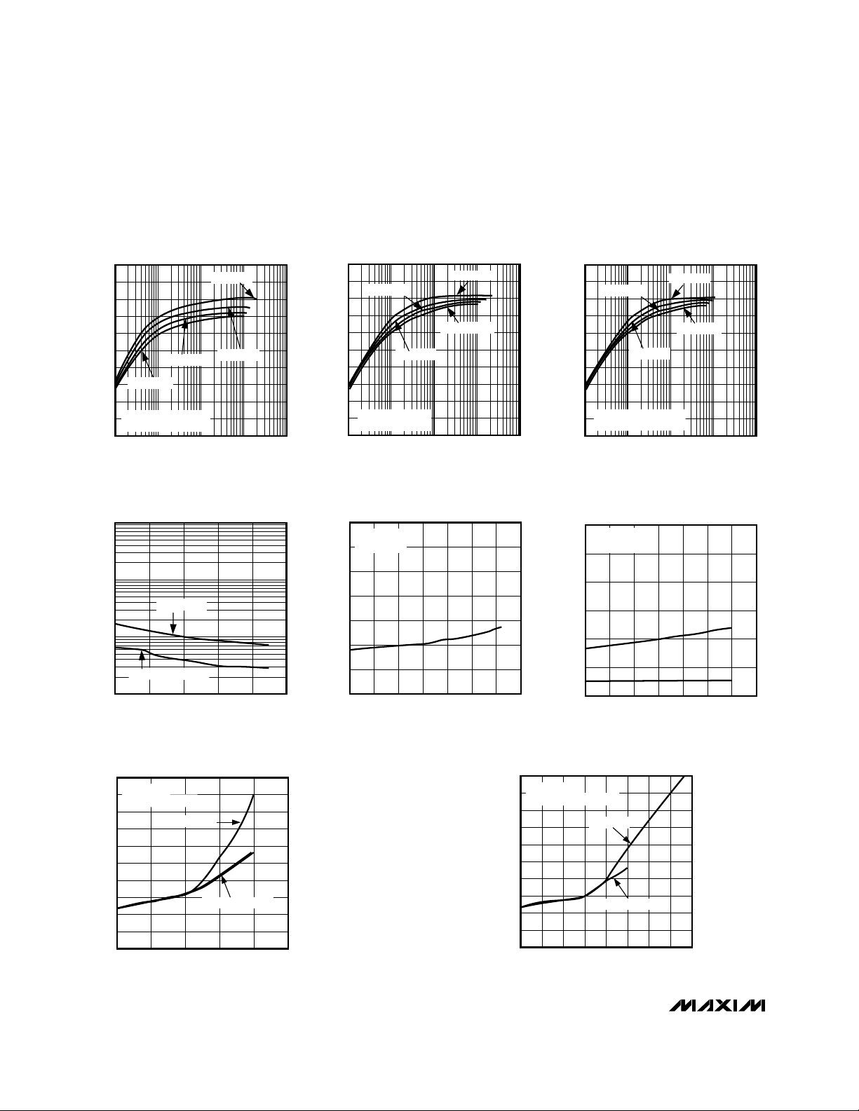
0.6
0
MINIMUM START-UP INPUT VOLTAGE
vs. OUTPUT CURRENT
0.7
0.8
MAX1642/43 TOC07b
OUTPUT CURRENT (mA)
START-UP INPUT VOLTAGE (V)
12 14
1.2
1.1
1.5
1.4
1.3
0.9
1.0
2 4 6 10
16
1.6
8
L1 = 150µH
TDK NLC565050T-151K
V
OUT
= 5V
V
OUT
= 2.4V, 3.3V
0.6
0
MINIMUM START-UP INPUT VOLTAGE
vs. OUTPUT CURRENT
0.7
0.8
MAX1642/43 TOC07a
OUTPUT CURRENT (mA)
START-UP INPUT VOLTAGE (V)
20
1.2
1.1
1.5
1.4
1.3
0.9
1.0
5 15 25
1.6
10
L1 = 100µH
SUMIDA CD54-101
V
OUT
= 5V
V
OUT
= 2.4V, 3.3V
____________________________Typical Operating Characteristics (continued)
(Circuit of Figure 4, V
BATT
= 1.2V, R1 + R2 = 1MΩ, TA = +25°C, unless otherwise noted.)
0
0.01 1 100.1 100
EFFICIENCY vs. OUTPUT CURRENT
(V
OUT
= 3.3V)
10
MAX1642/43 TOC02B
OUTPUT CURRENT (mA)
EFFICIENCY (%)
VIN = 1.6V
L1 = 150µH
TDK NLC565050T-151K
VIN = 1.2V
VIN = 0.85V
VIN = 1.0V
20
30
40
50
60
70
80
90
100
100
90
80
0
0.01 1 100.1 100
EFFICIENCY vs. OUTPUT CURRENT
(V
OUT
= 5.0V)
20
10
MAX1642/43 TOC03a
OUTPUT CURRENT (mA)
EFFICIENCY (%)
30
40
50
60
70
VIN = 1.6V
VIN = 0.85V
VIN = 1.0V
L1 = 100µH
SUMIDA CD54-101
VIN = 1.2V
100
90
80
0
0.01 1 100.1 100
EFFICIENCY vs. OUTPUT CURRENT
(V
OUT
= 5.0V)
20
10
MAX1642/43 TOC03b
OUTPUT CURRENT (mA)
EFFICIENCY (%)
30
40
50
60
70
VIN = 1.6V
VIN = 0.85V
VIN = 1.0V
L1 = 150µH
TDK NLC565050T-151K
VIN = 1.2V
10,000
10
0.8 1.0 1.4 1.8
NO-LOAD BATTERY CURRENT
vs. INPUT VOLTAGE
100
1000
MAX1642/43 TOC04
INPUT VOLTAGE (V)
QUIESCENT CURRENT (mA)
1.2 1.6
V
OUT
= 5.0V
V
OUT
= 2.5V OR 3.3V
0
-40
NO-LOAD BATTERY CURRENT
vs. TEMPERATURE
20
MAX1642/43 TOC05
TEMPERATURE (°C)
QUIESCENT CURRENT (µA)
60
100
120
80
40
60
-20 4020 80 100
140
0
V
BATT
= 1.2V
V
OUT
= 3.3V
0
-40
BATT AND OUT PIN QUIESCENT CURRENTS
vs. TEMPERATURE
5
MAX1642/43 TOC06
TEMPERATURE (°C)
QUIESCENT CURRENT (µA)
60
20
25
10
15
-20 4020 80 100
30
0
V
BATT
= 1.2V
V
OUT
= 3.6V
I
BATT
I
OUT
Page 5

MAX1642/MAX1643
High-Efficiency, Step-Up
DC-DC Converters for 1V Inputs
_______________________________________________________________________________________
5
____________________________Typical Operating Characteristics (continued)
(Circuit of Figure 4, V
BATT
= 1.2V, R1 + R2 = 1MΩ, TA = +25°C, unless otherwise noted.)
B
LOAD-TRANSIENT RESPONSE
MAX1642/43 TOC10
A
400µs/div
V
OUT
= 3.3V, V
BATT
= 1.2V
A: OUT, 20mV/div, 3.3V DC OFFSET
B: LOAD, 2mA to 20mA, 10mA/div
0
0.8
MAXIMUM OUTPUT CURRENT
vs. INPUT VOLTAGE
MAX1642/43 TOC08b
INPUT VOLTAGE (V)
MAXIMUM OUTPUT CURRENT (mA)
1.4
25
30
5
15
10
20
0.9 1.31.2
1.5 1.6
35
1.0 1.1
L1 = 100µH
SUMIDA CD54-101
V
OUT
= 5V
V
OUT
= 3.3V
V
OUT
= 2.4V
0
0.8
MAXIMUM OUTPUT CURRENT
vs. INPUT VOLTAGE
MAX1642/43 TOC08c
INPUT VOLTAGE (V)
MAXIMUM OUTPUT CURRENT (mA)
1.4
14
12
18
16
4
2
6
10
8
0.9 1.31.2
1.5 1.6
20
1.0 1.1
L1 = 150µH
TDK NLC565050T-151K
V
OUT
= 5V
V
OUT
= 3.3V
V
OUT
= 2.4V
C
SWITCHING WAVEFORMS
MAX1642/43 TOC09
B
A
10ms/div
V
OUT
= 3.3V, VIN = 1.2V, I
OUT
= 12mA
A: LX, 2V/div, L1 = TDK NLC565050T-151K
B: OUT, 20mV/div, 3.3V DC OFFSET
C: INDUCTOR CURRENT, 100mA/div
B
LINE-TRANSIENT RESPONSE
MAX1642/43 TOC11
A
400µs/div
V
OUT
= 3.3V, LOAD = 15mA
A: OUT, 50mV/div, 3.3V DC OFFSET
B: V
BATT
, 1V to 1.5V, 500mV/div
B
C
SHUTDOWN RESPONSE AND
INDUCTOR CURRENT
MAX1642/43 TOC12
A
10ms/div
V
OUT
= 3.3V, V
BATT
= 1.2V, I
OUT
= 5mA
A: OUT, 1V/div
B: INDUCTOR CURRENT, 200mA/div
C: SHDN, 2V/div
Page 6

MAX1642/MAX1643
High-Efficiency, Step-Up
DC-DC Converters for 1V Inputs
6 _______________________________________________________________________________________
______________________________________________________________Pin Description
_______________Detailed Description
The MAX1642/MAX1643 each consist of an internal 1Ω,
N-channel MOSFET power switch, a built-in synchronous rectifier that acts as the catch diode, an oscillator,
a reference, and PFM control circuitry (Figure 1).
These devices are optimized for applications with
power-management features that operate from one
alkaline cell, such as pagers, remote controls, and battery-powered instruments. They are designed to meet
the specific demands of the operating states characteristic of such systems:
1)
Primary battery is good and the load is active:
In
this state, the system draws tens of milliamperes,
and the MAX1642/MAX1643 typically offer 80% efficiency.
2)
Primary battery is good and the load is sleeping:
In
this state, the load is drawing hundreds of microamperes, and the DC-DC converter IC draws very low
quiescent current. In many applications, the load is
expected to be in this state most of the time.
Operating Principle
The MAX1642/MAX1643 employ a proprietary pulsefrequency-modulation (PFM) control scheme that combines the ultra-low quiescent current traditional of
pulse-skipping PFM converters with the high-load efficiency of pulse-width-modulation (PWM) converters.
The on-time and minimum off-times are varied as a
function of the input and output voltages:
where K is typically 25V-µs. This enables the
MAX1642/MAX1643 to maintain high efficiency over a
wide range of loads and input/output voltages. The DCDC converter is powered from the OUT pin.
t =
K
V
t =
1.2 x K
V - V
ON
BATT
OFF(MIN)
OUT BATT
6
7
8
4
—
5
2
1
MAX1643
GroundGND6
N-Channel MOSFET Switch Drain and P-Channel Synchronous-Rectifier DrainLX7
Power Output. Feedback input for fixed 3.3V operation and IC power input. Connect filter
capacitor close to OUT.
OUT8
Open-Drain Power-Fail Output. Sinks current when PFI drops below 614mV.
PFO
3
Active-Low Shutdown Input. Connect to BATT for normal operation.
SHDN
4
Feedback Input for adjustable-output operation. Connect FB to an external resistor voltage
divider between OUT and GND. Connect to GND for fixed-output operation.
FB5
Power-Fail Input. When the voltage on PFI drops below 614mV, PFO sinks current.
PFI2
IC Battery-Power Input. Sense input for BATTLO comparator (MAX1643 only).
BATT1
PIN
3
Open-Drain Battery-Low Output. When the voltage at BATT drops below 1V, BATTLO
sinks current.
BATTLO
—
MAX1642
FUNCTIONNAME
Page 7

MAX1642/MAX1643
High-Efficiency, Step-Up
DC-DC Converters for 1V Inputs
_______________________________________________________________________________________ 7
BATT
PFI
0.5REF
PFO
GND
OUT
REF
N
P
OUT 1.7V
FB
SHDN
LX
RFRDY
REF
REF
0.5REF
START-UP
OSCILLATOR
TIMING
TON
EN
PDRV
NDRV
TOFF
LOGIC
MAX1642
Figure 1. MAX1642 Functional Diagram
When the error comparator detects that the output
voltage is too low, it turns on the internal N-channel
MOSFET switch until the on-time is satisfied (see Figure
1 and the Standard Application Circuits, Figures 2 and
3). During the on-time, current ramps up in the inductor, storing energy in a magnetic field. When the MOSFET turns off, during the second half of each cycle, the
magnetic field collapses, causing the inductor voltage
to force current through the synchronous rectifier,
transferring the stored energy to the output filter capacitor and load. The output filter capacitor stores charge
while current from the inductor is high, then holds up
the output voltage until the second half of the next
switching cycle, smoothing power flow to the load.
Bootstrap DC-DC Block
The bootstrap block contains a low-voltage start-up
oscillator. This oscillator pumps up the output voltage
to approximately 1.7V, where the main DC-DC converter can operate. The oscillator is powered from the
BATT input and drives an NPN switch. During start-up,
the P-channel synchronous rectifier remains off and
either its body diode or an external diode is used as an
output rectifier. Reduce the load as needed to allow
start-up with input voltages below 2V (see
Typical
Operating Characteristics
).
Shutdown (MAX1642)
Pulling SHDN low places the MAX1642 in shutdown
mode (I
SHDN
= 2µA typical). In shutdown, the internal
switching MOSFET turns off, PFO goes highimpedance, and the synchronous rectifier turns off to
prevent reverse current from flowing from the output
back to the input. However, there is still a forward current path through the synchronous-rectifier body diode
from the input to the output. Thus, in shutdown, the output remains one diode drop below the battery voltage
(V
BATT
). To disable the shutdown feature, connect
SHDN (a logic input) to BATT.
Page 8

MAX1642/MAX1643
High-Efficiency, Step-Up
DC-DC Converters for 1V Inputs
8 _______________________________________________________________________________________
BATTLO
(MAX1643)
The MAX1643 contains an on-chip comparator for lowbattery detection. If the voltage at BATT drops below
1V, BATTLO sinks current. BATTLO is an open-drain
output. In combination with PFI/PFO, this allows monitoring of both the input and output voltages.
Reverse-Battery Protection
The MAX1642/MAX1643 can sustain/survive single-cell
battery reversal up to the package power-dissipation
limit. An internal 5Ω resistor in series with a diode limits
reverse current to less than 220mA, which prevents damage to the MAX1642/MAX1643. Prolonged operation
above 220mA reverse-battery current can degrade the
devices’ performance.
________________Design Information
Output Voltage Selection
The MAX1642/MAX1643 operate with a 3.3V ±4% or
adjustable output. To select fixed-voltage operation, connect FB to GND. For an adjustable output between 2V
and 5.2V, connect FB to a resistor voltage divider
between OUT and GND (Figure 4). FB regulates to 1.23V.
Since FB leakage is 10nA max, select feedback resistor
R2 in the 100kΩ to 1MΩ range. R1 is given by:
where V
REF
= 1.23V.
Power-Fail Detection
The MAX1642/MAX1643 have an on-chip comparator for
power-fail detection. This comparator can detect loss of
power at the input or output. If the voltage at PFI falls
below 614mV, the PFO output sinks current to GND.
Hysteresis at the power-fail input is 1%. The power-fail
monitor’s threshold is set by two resistors: R3 and R4
(Figure 5). Set the threshold using the following equation:
where V
TH
is the desired threshold of the power-fail
detector, and V
PFI
is the 614mV reference of the powerfail comparator. Since PFI leakage is 10nA max, select
feedback resistor R4 in the 100kΩ to 1MΩ range.
Low-Battery Start-Up
The MAX1642/MAX1643 are bootstrapped circuits with
a low-voltage start-up oscillator. They can start under
low-load conditions at lower battery voltages than at full
load. Once started, the output can maintain the load as
the battery voltage decreases below the start-up voltage (see
Typical Operating Characteristics
).
Inductor Selection
A 100µH inductor is recommended for most applications. The use of lower inductor values (down to
68µH) increases maximum output current. Higher values (up to 220µH) reduce peak inductor current and
consequent ripple and noise. The inductor’s saturationcurrent rating must exceed the peak current limit synthesized by the MAX1642/MAX1643’s timing
algorithms:
where K
MAX
= 35V-µs. The maximum recommended
I
PEAK
is 350mA. For best efficiency, inductor series
resistance should be less than 1Ω.
I =
K
L
PEAK
MAX
MIN
R3 = R4
V
V
- 1
TH
PFI
R1 = R2
V
V
- 1
OUT
REF
MAX1642
GND FB
BATT
PFI
3.3V
OUT
0.88V to 1.65V INPUT
100µH, 350mA
PF0
22µF0.1µF
SHDN
LX
OUT
OUT
22µF 0.1µF
Figure 2. MAX1642 3.3V Standard Application Circuit
Figure 3. MAX1643 3.3V Standard Application Circuit
0.88V to 1.65V INPUT
22µF
100µH, 350mA
0.1µF
BATT
OUT
MAX1643
BATTLO
GND FB
LX
OUT
PFI
PFO
3.3V
OUT
22µF0.1µF
Page 9

MAX1642/MAX1643
High-Efficiency, Step-Up
DC-DC Converters for 1V Inputs
_______________________________________________________________________________________ 9
Capacitor Selection
Choose input and output capacitors to service input
and output peak currents with acceptable voltage ripple. A 22µF, 6V, low-ESR, surface-mount tantalum output filter capacitor typically provides 60mV output
ripple when stepping up from 1.3V to 3.3V at 20mA.
The input filter capacitor (CIN) also reduces peak currents drawn from the battery and improves efficiency.
Low equivalent series resistance (ESR) capacitors are
recommended. Capacitor ESR is a major contributor to
output ripple (usually more than 60%). Ceramic capacitors have the lowest ESR, but low-ESR tantalums represent a good balance between cost and performance.
Low-ESR aluminum electrolytic capacitors are tolerable,
and standard aluminum electrolytic capacitors should
be avoided. Do not exceed tantalum capacitors’ ripplecurrent ratings; select capacitors with a rating exceeding the peak inductor current (I
PEAK
).
PC Board Layout and Grounding
High switching frequencies and large peak currents
make PC board layout an important part of design. Poor
design can result in excessive EMI on the feedback paths
and voltage gradients in the ground plane. Both of these
factors can result in instability or regulation errors. The
OUT pin must be bypassed directly to GND as close to
the IC as possible (within 0.2 in. or 5mm).
Place power components—such as the MAX1642/
MAX1643, inductor, input filter capacitor, and output filter
capacitor—as close together as possible. Keep their
traces short, direct, and wide (≥50 mil or 1.25mm), and
place their ground pins close together in a star-ground
configuration. Keep the extra copper on the board and
integrate it into ground as a pseudo-ground plane. On
multilayer boards, route the star ground using component-side copper fill, then connect it to the internal ground
plane using vias.
Place the external voltage-feedback network very close to
the FB pin (within 0.2 in. or 5mm). Noisy traces, such as
from the LX pin, should be kept away from the voltagefeedback network and separated from it using grounded
copper. The evaluation kit manual shows an example PC
board layout, routing, and pseudo-ground plane.
Noise and Voltage Ripple
EMI and output voltage ripple can be minimized by following a few simple design rules.
1) Place the DC-DC converter and digital circuitry on
an opposite corner of the PC board, away from sensitive RF and analog input stages.
2) Use a closed-core inductor, such as toroid or
shielded bobbin, to minimize fringe magnetic fields.
3) Choose the largest inductor value that satisfies the
load requirement to minimize peak switching current and resulting ripple and noise.
4) Use low-ESR input and output filter capacitors.
5) Follow sound circuit-board layout and grounding
rules (see the
PC Board Layout and Grounding
section).
6) Where necessary, add LC pi filters, linear post-regulators such as the MAX8863 and MAX8864
(SOT23 package), or shielding. The LC pi filter’s
cutoff frequency should be at least a decade or two
below the DC-DC converter’s switching frequency
for the specified load and input voltage.
MAX1642
GND
BATT
PFI
V
OUT
= 2V
TO 5.2V
0.88V to 1.65V INPUT
*OPTIONAL COMPENSATION
100µH
PF0
100pF*
SHDN
LX
OUT
FB
R1
R2
OUT
22µF 0.1µF
Figure 4. Adjustable-Output Circuit
Figure 5. Power-Fail Detection Circuit
V
TH
MAX1642
MAX1643
PFI
R3
R4
Page 10

MAX1642/MAX1643
High-Efficiency, Step-Up
DC-DC Converters for 1V Inputs
10 ______________________________________________________________________________________
Table 2. Surface-Mount Inductor Information
Table 1. Component Suppliers
SUPPLIER PHONE FAX
AVX USA
(803) 946-0690 (803) 626-3123
(800) 282-4975
Coilcraft USA (847) 639-6400 (847) 639-1469
Coiltronics USA (561) 241-7876 (561) 241-9339
Dale USA (605) 668-4131 (605) 665-1627
Nichicon
USA (847) 843-7500 (847) 843-2798
Japan 81-7-5231-8461 81-7-5256-4158
Sanyo
USA (619) 661-6835 (619) 661-1055
Japan 81-7-2070-6306 81-7-2070-1174
Sprague USA (603) 224-1961 (603) 224-1430
Sumida
USA (847) 956-0666 (847) 956-0702
Japan 81-3-3607-5111 81-3-3607-5144
TDK USA (847) 390-4373 (847) 390-4428
TRANSISTOR COUNT: 594
SUBSTRATE CONNECTED TO GND
__________________ Chip Information
Sumida CD54-221 1.57 350
220
I
SAT
(mA)
RESISTANCE
(Ω)
Coilcraft DO1608-154
Coilcraft DO1608-224 2.3 220
Sumida CD54-151 1.1
1.7
400
270
Coilcraft DO1608-104
Sumida CD54-101 0.7100
1.1
520
310
Sumida CD54-680 0.46
68
610
400
INDUCTOR SPECIFICATION
VENDOR/PART
Coilcraft DO1608-683
INDUCTANCE
(µH)
TDK NLC565050T-101K 1.6 250
0.75
150
TDK NLC565050T-151K 2.2 210
Page 11

MAX1642/MAX1643
High-Efficiency, Step-Up
DC-DC Converters for 1V Inputs
______________________________________________________________________________________ 11
________________________________________________________Package Information
8LUMAXD.EPS
Page 12

MAX1642/MAX1643
High-Efficiency, Step-Up
DC-DC Converters for 1V Inputs
12 ______________________________________________________________________________________
NOTES
 Loading...