

Page 1
General Description
________________
The MAX1640/MAX1641 CMOS, adjustable-output,
switch-mode current sources operate from a +5.5V to
+26V input, and are ideal for microprocessor-controlled
battery chargers. Charging current, maximum output
voltage, and pulse-trickle charge are programmed with
external resistors. Programming the off-time modifies
the switching frequency, suppressing undesirable harmonics in noise-sensitive circuits. The MAX1640’s highside current sensing allows the load to connect directly
to ground, eliminating ground-potential errors. The
MAX1641 incorporates a low-side current sense.
The MAX1640/MAX1641 step-down pulse-width-modulation (PWM) controllers use an external P-channel
MOSFET switch and an optional, external N-channel
MOSFET synchronous rectifier for increased efficiency.
An internal low-dropout linear regulator provides power
for the internal reference and circuitry as well as the
gate drive for the N-channel synchronous rectifier.
The MAX1640/MAX1641 are available in space-saving,
16-pin narrow QSOP packages.
________________________Applications
Battery-Powered Equipment
Laptop, Notebook, and Palmtop Computers
Handy Terminals
Portable Consumer Products
Cordless Phones
Cellular Phones
PCS Phones
Backup Battery Charger
____________________________Features
♦ 95% Efficiency
♦ +5.5V to +26V Input Supply Range
♦ 2V to 24V Adjustable-Output Voltage Range
♦ 100% Maximum Duty Cycle (Low Dropout)
♦ Up to 500kHz PWM Operation
♦ Optional Synchronous Rectifier
♦ 16-Pin QSOP Package
♦ Current-Sense Accuracy: 2% (MAX1641),
5.3% (MAX1640)
MAX1640/MAX1641
Adjustable-Output, Switch-Mode
Current Sources with Synchronous Rectifier
________________________________________________________________
Maxim Integrated Products
1
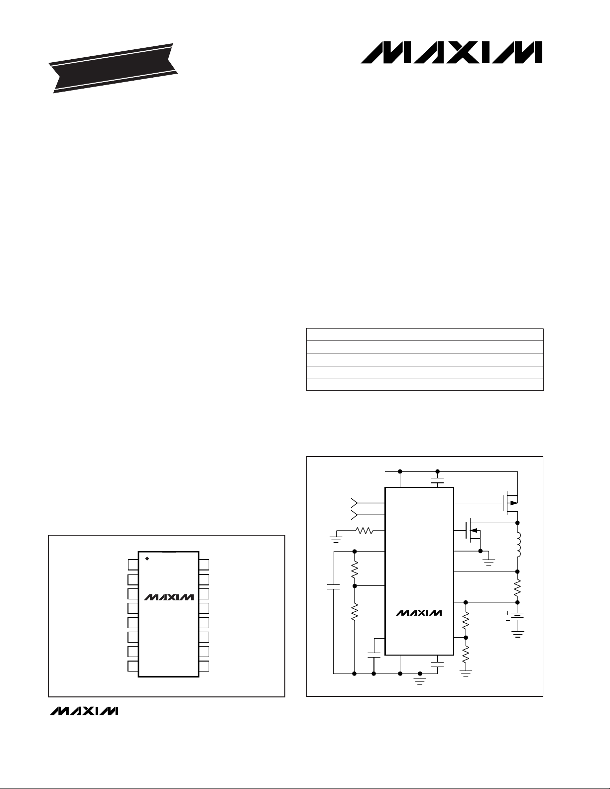
Pin Configuration
19-1245; Rev 1; 1/02
PART
MAX1640C/D
MAX1640EEE
MAX1641C/D
0°C to +70°C
-40°C to +85°C
0°C to +70°C
TEMP. RANGE PIN-PACKAGE
Dice*
16 QSOP
Dice*
__________________
______________________
Ordering Information
*
Dice are specified at T
A
= +25°C, DC parameters only.
MAX1641EEE -40°C to +85°C 16 QSOP
_____________
Typical Operating Circuit
EVALUATION KIT
AVAILABLE
For pricing, delivery, and ordering information, please contact Maxim/Dallas Direct! at
1-888-629-4642, or visit Maxim’s website at www.maxim-ic.com.
TOP VIEW
LDOL IN
1
TOFF
2
D1
3
MAX1640
4
D0
CC
REF
SET
TERM
5
6
7
8
MAX1641
16
15
14
13
12
11
10
9
LDOH
PDRV
NDRV
PGND
CS+
CS-
GND
V
= +5.5V TO +26V
IN
IN LDOH
D0
D1
R
TOFF
TOFF
REF
SET
MAX1640
CC
LDOLGND
PDRV
NDRV
PGND
CS+
CS-
TERM
OUT
P
QSOP
Page 2
MAX1640/MAX1641
Adjustable-Output, Switch-Mode
Current Source with Synchronous Rectifier
2 _______________________________________________________________________________________
ABSOLUTE MAXIMUM RATINGS
ELECTRICAL CHARACTERISTICS
(V
IN
= +12V, V
OUT
= 6V, Circuit of Figure 2, TA = 0°C to +85°C, unless otherwise noted. Typical values are at TA = +25°C.)
Stresses beyond those listed under “Absolute Maximum Ratings” may cause permanent damage to the device. These are stress ratings only, and functional
operation of the device at these or any other conditions beyond those indicated in the operational sections of the specifications is not implied. Exposure to
absolute maximum rating conditions for extended periods may affect device reliability.
Note 1: This ratio is generated by a 1:8 clock divider and is not an error source for current calculations.
IN to GND...............................................................-0.3V to +28V
LDOH to IN...............................................................+0.3V to -6V
LDOL to GND...........................................................-0.3V to +6V
PDRV to GND .............................. (V
LDOH
- 0.3V) to (VIN+ 0.3V)
NDRV to GND.........................................-0.3V to (V
LDOL
+ 0.3V)
TOFF, REF, SET, TERM, CC to GND ......-0.3V to (V
LDOL
+ 0.3V)
D0, D1 to GND .........................................................-0.3V to +6V
CS+, CS- to GND ...................................................-0.3V to +28V
PGND to GND.....................................................................±0.3V
Continuous Power Dissipation (TA = +70°C)
QSOP (derate 8.30mW/°C above +70°C)................... 667mW
Operating Temperature Range
MAX164_EEE...................................................-40°C to +85°C
Storage Temperature Range.............................-65°C to +150°C
Lead Temperature (soldering, 10sec)............................ +300°C
I
REF
= 0 to 50µA
D0 = D1 = low
D0 = D1 = low (off mode)
D0 or D1 = high
V
OUT
= 2V to 24V
VIN= V
OUT
+ 0.5V to 26V
MAX1641
MAX1641
MAX1640
VIN= 5.5V to 26V, I
LOAD
= 0 to 20mA
VIN= 5.5V to 26V, I
LOAD
= 0 to 20mA
MAX1640
CONDITIONS
µA1V
SET
Input Current
mV4 10Reference Load Regulation
V1.96 2.00 2.04V
REF
Reference Voltage
V4.05 4.20 4.35V
LDOL
Undervoltage Lockout
µA1Output Current in Off Mode
500
mA2 4
Quiescent VINSupply Current
0.1
%/V
0.1 0.4
Output Current Compliance
%/V0.03Current-Sense Line Regulation
34 37.5 41
mV
36 42 48
147 150 153
mV
142 150 158
Full-Scale Current-Sense
Threshold
V
VIN- VIN- VIN-
5.5 5.0 4.5
V
LDOH
Linear-Regulator Output
Voltage, VINReferenced
V4.5 5.0 5.5V
LDOL
Linear-Regulator Output
Voltage, Ground Referenced
UNITSMIN TYP MAXSYMBOLPARAMETER
V5.5 26V
IN
Input Voltage Range
FET Drive Output Resistance PFET and NFET drive 12 Ω
Off-Time Range 1 10 µs
Off-Time Accuracy R
TOFF
= 62kΩ 1.7 2.2 2.7 µs
Pulse-Trickle Mode Duty-Cycle
Period
D0 = low, D1 = high, R
TOFF
= 100kΩ 27 33 40 ms
Pulse-Trickle Mode Duty Cycle
(Note 1)
D0 = low, D1 = high, R
TOFF
= 100kΩ 12.5 %
Quarter-Scale Current-Sense
Threshold
MAX1640
MAX1641
µA
Page 3
MAX1640/MAX1641
Adjustable-Output, Switch-Mode
Current Source with Synchronous Rectifier
_______________________________________________________________________________________ 3
ELECTRICAL CHARACTERISTICS
(V
IN
= +12V, V
OUT
= 6V, Circuit of Figure 2, TA = -40°C to +85°C, unless otherwise noted.)
I
REF
= 0 to 50µA
V
OUT
= 2V to 24V (MAX1640)
D0 = D1 = low
D0 or D1 = high
FET Drive Output Resistance
MAX1641
MAX1640
VIN= 5.5V to 26V,
I
LOAD
= 0 to 20mA
VIN= 5.5V to 26V,
I
LOAD
= 0 to 20mA
MAX1640
CONDITIONS
µA1V
SET
Input Current
mV10Reference Load Regulation
V1.94 2.06V
REF
Reference Voltage
V4.0 4.4V
LDOL
Undervoltage Lockout
µA1Output Current in Off Mode
mA4Quiescent VINSupply Current
%/V0.4Output Current Compliance
mV
34 48
Quarter-Scale Current-Sense
Threshold
12 Ω
Off-Time Range
V5.5 26V
IN
Input Voltage Range
1.5 8 µs
Off-Time Accuracy R
TOFF
= 62kΩ 1.5 2.5 µs
146 154
Pulse-Trickle Mode Duty-Cycle
Period
mV
141 159
Full-Scale Current-Sense
Threshold
V
VIN- VIN-
5.5 4.5
V
LDOH
Linear-Regulator Output
Voltage, VINReferenced
D0 = low, D1 = high, R
TOFF
= 50kΩ 25 42 ms
V4.5 5.5V
LDOL
Linear-Regulator Output
Voltage, Ground Referenced
UNITSMIN TYP MAXSYMBOLPARAMETER
PWM Maximum Duty Cycle 100 %
Input Low Voltage V
IL
D0, D1 0.8 V
Input High Voltage V
IH
D0, D1 2.4 V
Input Leakage Current I
IN
D0, D1 ±1 µA
33 42MAX1641
ELECTRICAL CHARACTERISTICS (continued)
(V
IN
= +12V, V
OUT
= 6V, Circuit of Figure 2, TA = 0°C to +85°C, unless otherwise noted. Typical values are at TA = +25°C.)
CONDITIONS UNITSMIN TYP MAXSYMBOLPARAMETER
PWM Maximum Duty Cycle 100 %
Input Low Voltage V
IL
D0, D1 0.8 V
Input High Voltage V
IH
D0, D1 2.4 V
Input Leakage Current I
IN
D0, D1 ±1 µA
Page 4
MAX1640/MAX1641
Adjustable-Output, Switch-Mode
Current Source with Synchronous Rectifier
4 _______________________________________________________________________________________
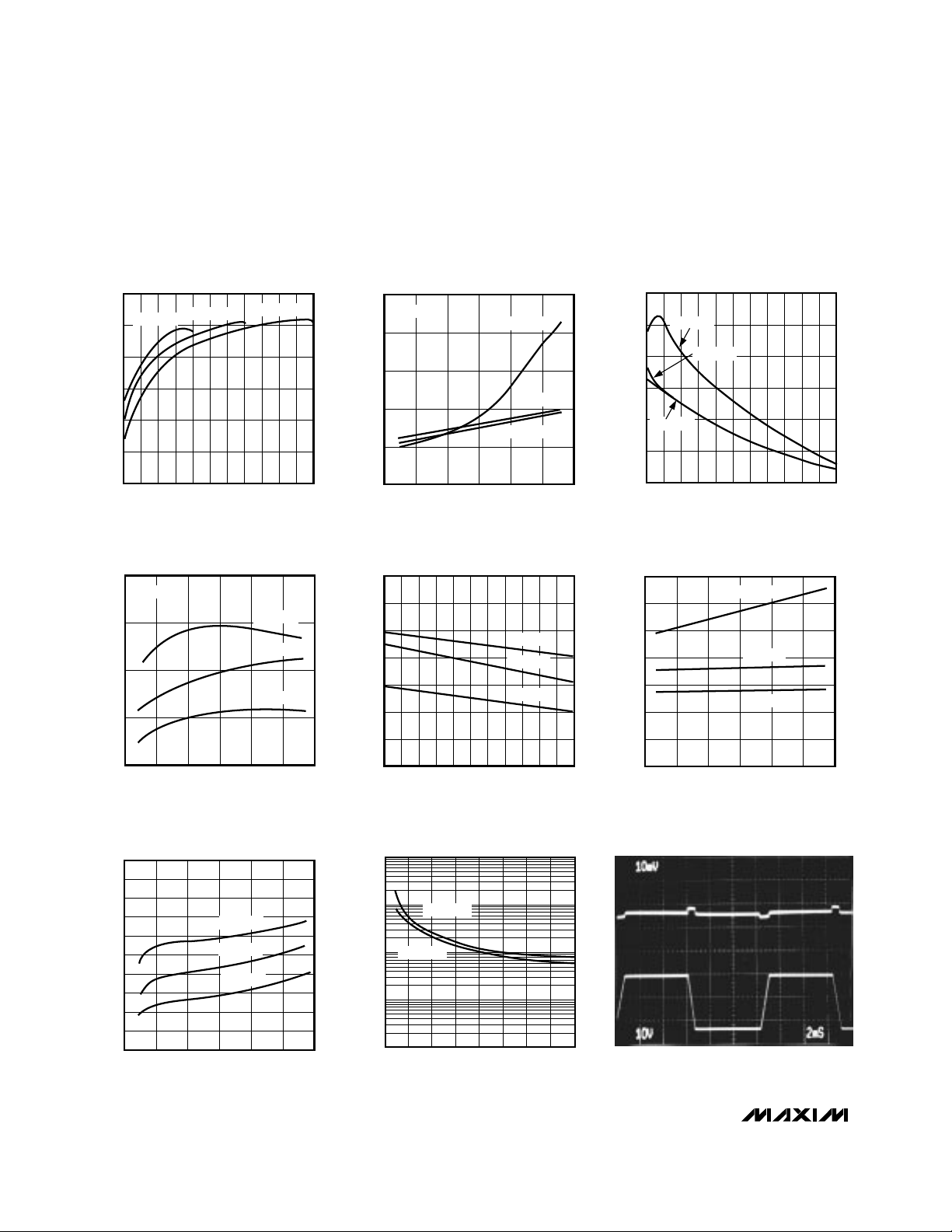
0.45
0.51
0.49
0.47
0.53
0.55
0.57
0.59
0.61
0.63
0.65
4 128 16 20 24 28
OFF-MODE SUPPLY CURRENT
(NO-LOAD)
MAX1640/41-TOC07
INPUT VOLTAGE (V)
OFF-MODE SUPPLY CURRENT (mA)
TA = -40°C
TA = +25°C
TA = +85°C
10,000
1
0 50 100 150 200 250 300 350 400
SWITCHING FREQUENCY vs. R
TOFF
MAX1640/41 TOC 08
T
OFF
(kΩ)
SWITCHING FREQUENCY (kHz)
10
100
1000
V
OUT
= +3V
V
OUT
= +6V
__________________________________________Typical Operating Characteristics
(Circuit of Figure 2, TA = +25°C, unless otherwise noted.)
40
60
50
80
70
90
100
2 6 8 104 12 14 16 18 20 22 24
EFFICIENCY vs. OUTPUT VOLTAGE
MAX1640/41-TOC01
OUTPUT VOLTAGE (V)
EFFICIENCY (%)
VIN = 12V
VIN = 18V
VIN = 26V
1.460
1.470
1.480
1.490
1.500
1.510
4 128 16 20 24 28
MAX1640
OUTPUT CURRENT vs. INPUT VOLTAGE
MAX1640/41 TOC02
INPUT VOLTAGE (V)
OUTPUT CURRENT (A)
TA = -40°C
(V
OUT
= 4V)
TA = +25°C
TA = +85°C
1.450
1.470
1.460
1.490
1.480
1.500
1.510
2 6 8 104 12 14 16 18 20 22 24
MAX1640
OUTPUT CURRENT vs. OUTPUT VOLTAGE
MAX1640/41-TOC03
OUTPUT VOLTAGE (V)
OUTPUT CURRENT (A)
TA = -40°C
TA = +85°C
TA = +25°C
1.450
1.475
1.500
1.525
1.550
4 128 16 20 24 28
MAX1641
OUTPUT CURRENT vs. INPUT VOLTAGE
MAX1640/41 TOC04
INPUT VOLTAGE (V)
OUTPUT CURRENT (A)
TA = -40°C
(V
OUT
= 4V)
TA = +25°C
TA = +85°C
1.420
1.460
1.440
1.500
1.480
1.540
1.520
1.560
2 6 8 104 12 14 16 18 20 22 24
MAX1641
OUTPUT CURRENT vs. OUTPUT VOLTAGE
MAX1640/41-TOC05
V
OUT
(V)
OUTPUT CURRENT (A)
TA = -40°C
TA = +25°C
TA = +85°C
1.5
1.9
1.7
2.1
2.3
2.5
2.7
2.9
4 128 16 20 24 28
QUIESCENT CURRENT
vs. INPUT VOLTAGE (NO-LOAD)
MAX1640/41-TOC06
INPUT VOLTAGE (V)
QUIESCENT CURRENT (mA)
TA = -40°C
TA = +25°C
TA = +85°C
A: OUTPUT CURRENT, D1 = D0 = 1 1A/div
V
LOAD
= 3V
B: INPUT VOLTAGE, 10V/div
LINE-TRANSIENT RESPONSE
A
B
0A
0V
2ms/div
MAX1640/41 TOC 09
Page 5

MAX1640/MAX1641
Adjustable-Output, Switch-Mode
Current Source with Synchronous Rectifier
_______________________________________________________________________________________ 5
____________________________Typical Operating Characteristics (continued)
(Circuit of Figure 2, TA = +25°C, unless otherwise noted.)
A: OUTPUT CURRENT, D0 = D1 = 0 1A/div
V
IN
= 12V, V
SET
= 1V, R
LOAD
= 4Ω, NO OUTPUT CAPACITOR
B: LOAD VOLTAGE, AC coupled, 500mV/div
CURRENT-MODE CHANGE RESPONSE TIME
A
B
2ms/div
0A
0V
MAX1640/41 TOC 10
B
A
EXITING OFF MODE
MAX1640/41 TOC11
A: D0 = D1 = 1 2V/div
V
IN
= 12V, R
LOAD
= 4Ω
B: OUTPUT CURRENT, 0.5A/div
20µs/div
______________________________________________________________Pin Description
NAME FUNCTION
1 LDOL
Internal, Ground-Referenced Low-Dropout Linear Regulator Output.
Bypass with a 0.1µF capacitor in parallel with a 4.7µF capacitor to GND.
2 TOFF
Off-Time Select Input. A resistor (R
TOFF
) connected from this pin to GND programs the off-time for the hys-
teretic PWM step-down converter. This resistor also sets the period in duty-cycle mode. See
Duty-Cycle
Mode and Programming the Off-Time.
PIN
3, 4 D1, D0 Digital Inputs. Select mode of operation (Table 1).
5 CC Constant-Current Loop Compensation Input. Bypass with a 0.01µF capacitor to GND.
8 TERM
Maximum Output Voltage Termination Input. When V
TERM
exceeds the reference voltage, the comparator
resets the internal PWM latch, shutting off the external P-channel FET.
7 SET
Current Select Input. Program the desired current level by applying a voltage at SET between 0V and V
REF
,
(I = V
SET
/ 13.3R
SENSE
). See Figure 3.
6 REF Reference Voltage Output (V
REF
= 2V). Bypass with a 0.1µF capacitor to GND.
13 NDRV Gate Drive for an Optional N-Channel FET Synchronous Rectifier
12 PGND High-Current Ground Return for the Output Drivers
11 CS+ Positive Current-Sense Comparator Input
10 CS- Negative Current-Sense Comparator Input
9 GND Ground
14 PDRV Gate Drive for the P-Channel FET
15 LDOH
Internal, Input-Referenced Low-Dropout Linear Regulator Output.
Bypass with a 0.33µF capacitor to IN.
16 IN Power-Supply Input. Input of the internal, low-dropout linear regulators.
Page 6

MAX1640/MAX1641
Adjustable-Output, Switch-Mode
Current Source with Synchronous Rectifier
6 _______________________________________________________________________________________
MODE
CONTROL
CC TOFFD0, D1
TERM
REF
SET
CS-
CS+
REG
PDRV
NDRV
PGND
IN
LDOL
LDOH
A1
A2
Gm
MUX
B
A
SEL
MAX1640
MAX1641
Figure 1. MAX1640/MAX1641 Functional Diagram
Page 7

MAX1640/MAX1641
Adjustable-Output, Switch-Mode
Current Source with Synchronous Rectifier
_______________________________________________________________________________________ 7
_______________Detailed Description
The MAX1640/MAX1641 switch-mode current sources
utilize a hysteretic, current-mode, step-down pulsewidth-modulation (PWM) topology with constant offtime. Internal comparators control the switching
mechanism. These comparators monitor the current
through a sense resistor (R
SENSE
) and the voltage at
TERM. When inductor current reaches the current limit
[(V
CS+
- V
CS-
) / R
SENSE
], the P-channel FET turns off
and the N-channel FET synchronous rectifier turns on.
Inductor energy is delivered to the load as the current
ramps down. This ramp rate depends on R
TOFF
and
inductor values. When off-time expires, the P-channel
FET turns back on and the N-channel FET turns off.
Two digital inputs, D0 and D1, select between four possible current levels (Table 1). In pulse-trickle mode, the
part operates for 12.5% of the period set by R
TOFF
,
resulting in a lower current for pulse-trickle charging.
Figure 1 is the MAX1640/MAX1641 functional diagram.
Figure 2 shows the standard application circuits.
Charge Mode: Programming the
Output Currents
The sense resistor, R
SENSE
, sets two charging current
levels. Choose between these two levels by holding
D0 high, and toggling D1 either high or low (Table 1).
The fast-charge current level equals VCS/ R
SENSE
where VCSis the full-scale current-sense voltage of
150mV. Alternatively, calculate this current by V
REF
/
(13.3R
SENSE
). The top-off current equals V
SET
/
(13.3R
SENSE
). A resistor-divider from REF to GND pro-
grams the voltage at SET (Figure 3).
P
N
0.1µF
4.7µF
47µF
0.33µF
0.01µF
0.1µF
R1
R
TOFF
R2
SET
REF
TOFF
D1
D0
LDOL
PDRV
NDRV
PGND
CS+
CS-
TERM
GNDCC
R3
47µH
V
OUT
BATT
1/2 IR7309
1/2 IR7309
R4
100mΩ
LDOHIN
MAX1641
Figure 2a. Standard Application Circuit Figure 2b. Standard Application Circuit
47µF
0.33µF
4.7µF
0.1µF
R1
R2
0.1µF
R
TOFF
0.01µF
LDOL
D0
D1
TOFF
REF
SET
LDOHIN
MAX1640
GNDCC
PDRV
NDRV
PGND
CS+
CS-
TERM
1/2 IR7309
R3
R4
1/2 IR7309
N
P
47µH
100mΩ
V
OUT
BATT
Page 8

MAX1640/MAX1641
The voltage at SET is given by:
R1 = R2 (V
REF
/ V
SET
-1 ); 10kΩ < R2 < 300kΩ
where V
REF
= 2V and V
SET
is proportional to the
desired output current level.
The MAX1640/MAX1641 are specified for V
SET
between 0V and V
REF
. For V
SET
> V
REF
, output current
increases linearly (with reduced accuracy) until it
clamps at V
SET
≈ 4V.
Pulse-Trickle Mode: Selecting the
Pulse-Trickle Current
Pulling D0 low and D1 high selects pulse-trickle mode.
This current equals V
SET
/ (13.3R
SENSE
) and remains
on for 12.5% of the period set by R
TOFF
. Pulse-trickle
current maintains full charge across the battery and
can slowly charge a cold battery before fast charging
commences.
Off Mode: Turning Off the Output Current
Pulling D0 and D1 low turns off the P-channel FET and
hence the output current flow. This mode also controls
end of charge and protects the battery against excessive temperatures.
Setting the Maximum Output
Voltage Level
The maximum output voltage should be programmed to
a level higher than the output/battery voltage (I
LOAD
x
R
LOAD
). An external resistor-divider between the output
and ground (Figure 4) sets the voltage at TERM. Once
the voltage at TERM exceeds the reference, the internal
comparator turns off the P-channel FET, terminating
current flow. Select R4 in the 10kΩ to 500kΩ range.
R3 is given by:
R3 = R4 (V
OUT
/ V
TERM
) -1
PERIOD = 3.2 x 10 x R (sec)
-7
TOFF
Adjustable-Output, Switch-Mode
Current Source with Synchronous Rectifier
8 _______________________________________________________________________________________
D1 DO MODE
OUTPUT CURRENT (A)
0 0 OFF 0
0 1 Top-Off V
SET
/ (13.3R
SENSE
)
1 0 Pulse-Trickle
V
SET
/ (13.3R
SENSE
)
12.5% duty cycle
1 1 Fast Charge V
REF
/ (13.3R
SENSE
)
Table 1. Selecting Output Current Levels
MAX1640
MAX1641
REF
SET
R1
R2
Figure 3. Adjusting the Output Current Level
MAX1640
CS+
TERM
CS-
R3
R
SENSE
BATT
L
R4
Figure 4a. Setting the Maximum Output Voltage Level
MAX1641
CS+
TERM
CS-
R3
BATT
R4
R
SENSE
L
Figure 4b. Setting the Maximum Output Voltage Level
Page 9

where V
TERM
= 2V and V
OUT
is the desired output
voltage.
Programming the Off-Time
When programming the off-time, consider such factors
as maximum inductor current ripple, maximum output
voltage, inductor value, and inductor current rating. The
output current ripple is less than the inductor current ripple and depends heavily on the output capacitor’s size.
Perform the following steps to program the off-time:
1) Select the maximum output current ripple. IR(A)
2) Select the maximum output voltage. V
OUT
(MAX)(V)
3) Calculate the inductor value range as follows:
L
MIN
= (V
OUTMAX
x 1µs) / I
R
L
MAX
= (V
OUTMAX
x 10µs) / I
R
4) Select an inductor value in this range.
5) Calculate t
OFF
as follows:
6) Program t
OFF
by selecting R
TOFF
from:
R
TOFF
= (29.3 x 10⁹) x t
OFF
7) Calculate the switching frequency by:
fs = 1 / (tON+ t
OFF
)
where tON= (IRx L) / (VIN- V
OUT
) and IR= (V
OUT
x
t
OFF
) / L. L is the inductor value, VINis the input volt-
age, V
OUT
is the output voltage, and IRis the output
peak-to-peak current ripple.
Note that R
TOFF
sets both the off-time and the pulse-
trickle charge period.
Reference
The on-chip reference is laser trimmed for a precise 2V
at REF. REF can source no more than 50µA. Bypass
REF with a 0.1µF capacitor to ground.
Constant-Current Loop: AC Loop
Compensation
The constant-current loop’s output is brought out at CC.
To reduce noise due to variations in switching currents,
bypass CC with a 1nF to 100nF capacitor to ground. A
large capacitor value maintains a constant average output current but slows the loop response to changes in
switching current. A small capacitor value speeds up
the loop response to changes in switching current,
generating increased ripple at the output. Select C
CC
to optimize the ripple vs. loop response.
Synchronous Rectification
Synchronous rectification reduces conduction losses in
the rectifier by shunting the Schottky diode with a lowresistance MOSFET switch. In turn, efficiency increases
by about 3% to 5% at heavy loads. To prevent crossconduction or “shoot-through,” the synchronous rectifier
turns on shortly after the P-channel power MOSFET
turns off. The synchronous rectifier remains off for 90%
of the off-time. In low-cost designs, the synchronous
rectifier FET may be replaced by a Schottky diode.
Component Selection
External Switching Transistors
The MAX1640/MAX1641 drive an enhancement-mode
P-channel MOSFET and a synchronous-rectifier Nchannel MOSFET (Table 2).
When selecting a P-channel FET, some important parameters to consider are on-resistance (r
DS(ON)
), maximum drain-to-source voltage (VDSmax), maximum
gate-to-source voltage (VGSmax), and minimum
threshold voltage (V
TH
min).
In high-current applications, MOSFET package power
dissipation often becomes a dominant design factor.
I2R power losses are the greatest heat contributor for
both high-side and low-side MOSFETs. Switching losses affect the upper MOSFET only (P-channel), since the
Schottky rectifier or the N-FET body diode clamps the
switching node before the synchronous rectifier turns on.
Rectifier Diode
If an N-channel MOSFET synchronous rectifier is not
used, a Schottky rectifier is needed. The MAX1640/
t =
L x I
V
OFF
R
OUTMAX
MAX1640/MAX1641
Adjustable-Output, Switch-Mode
Current Source with Synchronous Rectifier
_______________________________________________________________________________________ 9
Table 2. Component Manufacturers
COMPONENT MANUFACTURER
MOSFETs
Sense Resistor
Capacitors
International Rectifier
Dale
AVX
Sumida
Coilcraft
Inductor
Coiltronics
Siliconix S14539DY
IRF7309
WSL-2010 series
TPS series
MBAR5340t3
CDRH125 series
D03316P series
UP2 series
IRC LR2010-01 series
Sprague 595D series
Nihon NSQ03A04
Rectifier
IN5817-IN5822
Motorola
Page 10

MAX1640/MAX1641
MAX1641’s high switching frequency demands a highspeed rectifier (Table 2). Schottky diodes such as the
1N5817–1N5822 are recommended. Make sure the
Schottky diode’s average current rating exceeds the
peak current limit and that its breakdown voltage
exceeds the output voltage (V
OUT
). For high-temperature applications, Schottky diodes may be inadequate
due to their high leakage current; high-speed silicon
diodes such as the MUR105 or EC11FS1 can be used
instead. At heavy loads and high temperatures, the
benefits of a Schottky diode’s low forward voltage may
outweigh the disadvantage of high leakage current. If
the application uses an N-channel MOSFET synchronous rectifier, a parallel Schottky diode is usually
unnecessary except with very high charge current (> 3
amps). Best efficiency is achieved with both an
N-channel MOSFET and a Schottky diode.
Inductor Value
Refer to the section
Programming the Off-Time
to select
the proper inductor value. There is a trade-off between
inductor value, off-time, output current ripple, and
switching frequency.
__________Applications Information
All-Purpose Microcontroller Battery
Charger: NiCd, NiMH
In applications where a microcontroller is available, the
MAX1640/MAX1641 can be used as a low-cost battery
charger (Figure 5). The controller takes over fast
charge, pulse-trickle charge, charge termination, and
other smart functions. By monitoring the output voltage
at V
OUT
, the controller initiates fast charge (set D0 and
D1 high), terminates fast charge and initiates top-off
(set D0 high and D1 low), enters trickle charge (set D0
low and D1 high), or shuts off and terminates current
flow (set D0 and D1 low).
Layout and Grounding
Due to high current levels and fast switching waveforms, proper PC board layout is essential. High-current ground paths should be connected in a star
Adjustable-Output, Switch-Mode
Current Source with Synchronous Rectifier
10 ______________________________________________________________________________________
P
N
D1
D0
T
I/0
I/0
CH1
CH0
PDRV
NDRV
PGND
CS+
CS-
R3
R4
TERM
GND
LOW-SIDE IS SHORTED
DC IN
R
SENSE
MAX1640
BATT
Figure 5. Microcontroller Battery Charger
Page 11

configuration to PGND. These traces should be wide to
reduce resistance and as short as possible to reduce
stray inductance. All low-current ground paths should
be connected to GND. Place the input bypass capacitor as close as possible to the IN pin. See MAX1640 EV
kit for layout example.
MAX1640/MAX1641
Adjustable-Output, Switch-Mode
Current Source with Synchronous Rectifier
___________________Chip Information
TRANSISTOR COUNT: 1233
QSOP.EPS
Maxim cannot assume responsibility for use of any circuitry other than circuitry entirely embodied in a Maxim product. No circuit patent licenses are
implied. Maxim reserves the right to change the circuitry and specifications without notice at any time.
Maxim Integrated Products, 120 San Gabriel Drive, Sunnyvale, CA 94086 408-737-7600 _____________________ 11
© 2002 Maxim Integrated Products Printed USA is a registered trademark of Maxim Integrated Products.
Package Information
(The package drawing(s) in this data sheet may not reflect the most current specifications. For the latest package outline information,
go to www.maxim-ic.com/packages.)
 Loading...