

Page 1
________________General Description
The MAX1639 is an ultra-high-performance, step-down
DC-DC controller for CPU power in high-end computer
systems. Designed for demanding applications in which
output voltage precision and good transient response are
critical for proper operation, it delivers over 35A from 1.1V
to 4.5V with ±1% total accuracy from a +5V ±10% supply.
Excellent dynamic response corrects output transients
caused by the latest dynamically clocked CPUs. This
controller achieves over 90% efficiency by using synchronous rectification. Flying-capacitor bootstrap circuitry
drives inexpensive, external N-channel MOSFETs.
The switching frequency is pin-selectable for 300kHz,
600kHz, or 1MHz. High switching frequencies allow the
use of a small surface-mount inductor and decrease output filter capacitor requirements, reducing board area
and system cost.
Output overvoltage protection is enforced by a crowbar
circuit that turns on the low-side MOSFET with 100%
duty factor when the output is 200mV above the normal
regulation point. Other features include internal digital
soft-start, a power-good output, and a 3.5V ±1% reference output. The MAX1639 is available in a 16-pin
narrow SOIC package.
________________________Applications
Local DC-DC Converters for CPUs
Workstations
Desktop Computers
LAN Servers
GTL Bus Termination
____________________________Features
♦ Better than ±1% Output Accuracy Over
Line and Load
♦ Greater than 90% Efficiency Using N-Channel
MOSFETs
♦ Pin-Selected High Switching Frequency:
300kHz, 600kHz, or 1MHz
♦ Over 35A Output Current
♦ Resistor-Divider Adjustable Output from
1.1V to 4.5V
♦ Current-Mode Control for Fast Transient
Response and Cycle-by-Cycle Current-Limit
Protection
♦ Short-Circuit Protection with Foldback Current
Limiting
♦ Crowbar Overvoltage Protection
♦ Power-Good (PWROK) Output
♦ Digital Soft-Start
♦ High-Current (2A) Drive Outputs
MAX1639
High-Speed Step-Down Controller with
Synchronous Rectification for CPU Power
________________________________________________________________
Maxim Integrated Products
1
19-1337; Rev 0; 2/98
PART
MAX1639ESE -40°C to +85°C
TEMP. RANGE PIN-PACKAGE
16 Narrow SO
_______________Ordering Information
__________
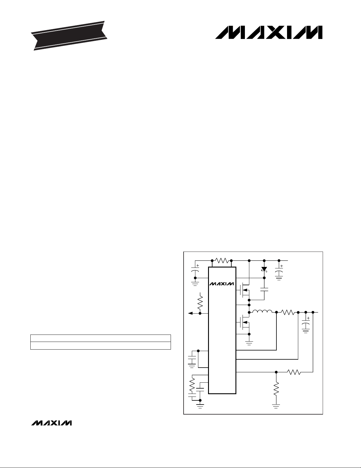
Typical Operating Circuit
Pin Configuration appears at end of data sheet.
V
CC
AGND
REF
FREQ
CC1
CC2
DL
PWROK
LX
BST
DH
PGND
TO V
DD
CSH
OUTPUT
1.1V TO 4.5V
INPUT
+5V
V
DD
CSL
FB
MAX1639
For free samples & the latest literature: http://www.maxim-ic.com, or phone 1-800-998-8800.
For small orders, phone 408-737-7600 ext. 3468.
EVALUATION KIT
AVAILABLE
Page 2
FREQ Input Voltage
MAX1639
High-Speed Step-Down Controller with
Synchronous Rectification for CPU Power
2 _______________________________________________________________________________________
ABSOLUTE MAXIMUM RATINGS
ELECTRICAL CHARACTERISTICS
(VDD= VCC= +5V, PGND = AGND = 0V, FREQ = REF, TA= 0°C to +85°C, unless otherwise noted.)
Stresses beyond those listed under “Absolute Maximum Ratings” may cause permanent damage to the device. These are stress ratings only, and functional
operation of the device at these or any other conditions beyond those indicated in the operational sections of the specifications is not implied. Exposure to
absolute maximum rating conditions for extended periods may affect device reliability.
VDD, VCC, PWROK to AGND....................................-0.3V to +6V
PGND to AGND ..................................................................±0.3V
CSH, CSL to AGND....................................-0.3V to (VCC+ 0.3V)
DL to PGND................................................-0.3V to (VDD+ 0.3V)
REF, CC1, CC2, FREQ, FB to AGND .........-0.3V to (V
CC
+ 0.3V)
BST to PGND..........................................................-0.3V to +12V
BST to LX..................................................................-0.3V to +6V
DH to LX.............................................(LX - 0.3V) to (BST + 0.3V)
Continuous Power Dissipation (TA= +70°C)
16-Pin Narrow SO (derate 8.70mW/°C above +70°C) ....696mW
SO θJC...........................................................................65°C/W
Operating Temperature Range
MAX1639ESE....................................................-40°C to +85°C
Storage Temperature Range.............................-65°C to +160°C
Lead Temperature (soldering, 10sec).............................+300°C
FREQ = AGND
FREQ = REF
VCC= V
DD
FREQ = V
CC
PWROK = 5.5V
Includes line and load
regulation errors
I
SINK
= 2mA, VCC= 4.5V
Falling FB, 1% hysteresis with respect to V
REF
Rising FB, 1% hysteresis with respect to V
REF
0µA < I
REF
< 100µA
No load
VCC= VDD= 5.5V, FB forced 60mV above
regulation point, operating or standby mode
VCCrising edge, 1% hysteresis
V
REF
= 0V
Rising edge, 1% hysteresis
CONDITIONS
kHz
255 300 345
Switching Frequency 540 600 660
850 1000 1150
µA1PWROK Output Current High
V0.4PWROK Output Voltage Low
%
6.5 8 9.5
PWROK Trip Level
-7.5 -6 -4.5
mA0.5 4.0Reference Short-Circuit Current
V2.7 3.0Reference Undervoltage Lockout
V4.5 5.5Input Voltage Range
V
1.083 1.117
1.089 1.111
FB Voltage
mV10Reference Load Regulation
V3.465 3.5 3.535Reference Voltage
mA0.1VDDSupply Current (IDD)
V4.0 4.2Input Undervoltage Lockout
UNITSMIN TYP MAXPARAMETER
TA= +25°C to +85°C
TA= 0°C to +85°C
2.5
5
CSH - CSL = 0mV to 80mV %1AC Load Regulation
CSH - CSL = 0mV to 80mV %0.1DC Load Regulation
FB overdrive = 60mV
FB overdrive = 0V
Operating
mode
mA
3.6 10
VCC= V
DD
= 5.5V
V
REF
= 0V
Shutdown
mode
VCCSupply Current (ICC)
VCC(high)
GND (low)
FREQ = V
CC
%
VCC- 0.1
Maximum Duty Cycle
0.2
85 90
FREQ Input Voltage V
REF (mid) 3.3 3.7
Page 3
ELECTRICAL CHARACTERISTICS (continued)
(VDD= V
CC
= +5V, PGND = AGND = 0V, FREQ = REF, TA= 0°C to +85°C, unless otherwise noted.)
MAX1639
_______________________________________________________________________________________
3
High-Speed Step-Down Controller with
Synchronous Rectification for CPU Power
15 38 70
mV
FB = 0V (foldback)
Current-Limit Trip Voltage
DL On-Resistance Ω
50 µABST = 12V, LX = 7V, REF = GNDBST Leakage Current
1536 1 / f
OSC
To full current limitSoft-Start Time
85 100 115FB = 1.1V
FB Input Current
CC2 Clamp Voltage
PARAMETER MIN TYP MAX UNITS
FREQ Input Current 4 µA
±0.1 µA
2.4 3.0
V
4 V
CC
CC2 Source/Sink Current 100 µA
0.7 2DH On-Resistance
Maximum
0.7 2
Ω
DH, DL Source/Sink Current 2 A
DH, DL Dead Time 0 30 ns
CONDITIONS
Minimum
30mV overdrive
BST - LX = 4.5V
VDD= 4.5V
DH = DL = 2.5V
ELECTRICAL CHARACTERISTICS
(VDD= VCC= +5V, PGND = AGND = 0V, FREQ = REF, TA= -40°C to +85°C, unless otherwise noted.) (Note 1)
Note 1: Specifications from 0°C to -40°C are guaranteed by design, not production tested.
FREQ = REF
FREQ = V
CC
BST - LX = 4.5V
FREQ = V
CC
Falling FB, 1% hysteresis with respect to V
REF
Rising FB, 1% hysteresis with respect to V
REF
FREQ = AGND
VDD= 4.5V
Ω2
%84
DL On-Resistance
VCCrising edge, 1% hysteresis
Ω
VCC= V
DD
2
CONDITIONS
510 690
Maximum Duty Cycle
800 1200
DH On-Resistance
Switching Frequency
FB = 1.1VCurrent-Limit Trip Voltage mV70 130
6 10
kHz
240 360
%
-8 -4
PWROK Trip Level
V3.9 4.3Input Undervoltage Range
V4.5 5.5Input Voltage Range
UNITSMIN TYP MAXPARAMETER
CC2 Transconductance
CC1 Output Resistance 10 kΩ
1 mmho
CSH, CSL Input Current 50 µACSH = CSL = 1.1V
VCC= VDD=
5.5V
mA
12
VDDSupply Current
3
Includes line and load regulation errors
No load
V1.072 1.128FB Voltage
V3.448 3.553Reference Voltage
VCC= VDD= 5.5V, FB forced 60mV above
regulation point, operating or shutdown mode
mA0.2VDDSupply Current
Operating mode FB overdrive = 60mV
VREF = 0VShutdown mode
Page 4
MAX1639
High-Speed Step-Down Controller with
Synchronous Rectification for CPU Power
4 _______________________________________________________________________________________
FOLDBACK CURRENT LIMIT
(V
OUT
= 2.5V, NOMINAL)
MAX1639-02
A: V
OUT
= 0.5V/div
B: INDUCTOR CURRENT, 5A/div
A
B
10µs/div
START-UP WAVEFORMS
MAX1639-03
A: INDUCTOR CURRENT, 2A/div
B: V
OUT
= 1V/div
A
B
400µs/div
1µs/div
SWITCHING WAVEFORMS
C
0
MAX1639-04
VIN = 5V, V
OUT
= 2.5V, LOAD = 0A
A: V
OUT
, 20mV/div
B: INDUCTOR CURRENT, 2A/div
C: LX, 5V/div
B
A
LOAD-TRANSIENT RESPONSE
(V
OUT
= 2.5V)
MAX1639-01
VIN = 5V, V
OUT
= 2.5V, LOAD = 8A
A: V
OUT
, 100mV/div, AC COUPLED
B: INDUCTOR CURRENT, 5A/div
A
B
10µs/div
__________________________________________Typical Operating Characteristics
(TA = +25°C, using the MAX1639 evaluation kit, unless otherwise noted.)
100
50
0.1 10
EFFICIENCY vs. OUTPUT CURRENT
60
90
80
70
MAX1639-05
OUTPUT CURRENT (A)
EFFICIENCY (%)
1
3.5V
1.8V
2.5V
50
55
0
MAXIMUM DUTY CYCLE vs.
SWITCHING FREQUENCY
65
60
70
MAX1639-06
SWITCHING FREQUENCY (kHz)
MAXIMUM DUTY CYCLE (%)
85
95
90
75
80
200 800 1000 1200
100
600400
Page 5

MAX1639
High-Speed Step-Down Controller with
Synchronous Rectification for CPU Power
_______________________________________________________________________________________ 5
______________________________________________________________Pin Description
7 Analog GroundAGND
6
Reference Output, 3.5V. Bypass REF to AGND with 0.1µF (min). Sources up to 100µA for external
loads. Force REF below 2V to turn off the controller.
REF
5 Analog Supply Input, 5V. Use an RC filter network, as shown in Figure 1. V
CC
4 Current-Sense Amplifier’s Noninverting InputCSH
3
Current-Sense Amplifier’s Inverting Input. Place the current-sense resistor very close to the controller IC,
and use a Kelvin connection.
CSL
2
Open-Drain Logic Output. PWROK is high when the voltage on FB is within +8% and -6% of its setpoint.
PWROK
8 Voltage-Feedback Input. The voltage at this input is regulated to 1.100V.FB
9
Fast-Loop Compensation Capacitor Input. Connect a ceramic capacitor and resistor in series from
CC1 to AGND. See the section
Compensating the Feedback Loop
.
CC1
FUNCTIONNAME
1
Boost-Capacitor Bypass for High-Side MOSFET Gate Drive. Connect a 0.1µF capacitor and low-leakage Schottky diode as a bootstrapped charge-pump circuit to derive a 5V gate drive from VDDfor DH.
BST
10
Slow-Loop Compensation Capacitor Input. Connect a ceramic capacitor from CC2 to AGND. See the
section
Compensating the Feedback Loop.
CC2
11
Frequency-Select Input. FREQ = VCC: 1MHz
FREQ = REF: 600kHz
FREQ = AGND: 300kHz
FREQ
12
Power Input for MOSFET Drivers, 5V. Bypass VDDto PGND within 0.2 in. (5mm) of the VDDpin using a
0.1µF capacitor and 4.7µF capacitor connected in parallel.
V
DD
13
Low-Side Synchronous Rectifier Gate-Drive Output. DL swings between PGND and VDD. See the
section
BST High-Side Gate-Driver Supply and MOSFET Drivers
.
DL
14 PGND Power Ground
15 LX Switching Node. Connect LX to the high-side MOSFET source and inductor.
16 DH
High-Side Main MOSFET Switch Gate-Drive Output. DH is a floating driver output that swings from LX
to BST, riding on the LX switching-node voltage. See the section
BST High-Side Gate-Driver Supply
and MOSFET Drivers
.
PIN
Page 6

MAX1639
High-Speed Step-Down Controller with
Synchronous Rectification for CPU Power
6 _______________________________________________________________________________________
N1
N2
D1
(OPTIONAL)
R3
(OPTIONAL)
R4
(OPTIONAL)
V
CC
V
DD
PWROK
BST
DH
LX
DL
PGND
CSH
FB
AGND
R8
C8
R7
CC1
CC2
CC1
1000pF
CC2
0.056µF
REF
C4, 1.0µF
CERAMIC
RC1
1k
TO
AGND
R6
100k
C5
0.1µF
C6
10µF
R5
10Ω
TO V
DD
FREQ
C7
0.1µF
D2
CMPSH-3
C3
0.1µF
L1
R1
V
IN
= 4.5V
TO 5.5V
C1
C2
MAX1639
V
OUT
= 1.1V
TO 4.5V
CSL
Figure 1. Standard Application Circuit
_______Standard Application Circuits
The predesigned MAX1639 circuit shown in Figure 1
meets a wide range of applications with output currents
up to 35A. Use Table 1 to select components appropriate for the desired output current range, and adapt the
evaluation kit PC board layout as necessary. This circuit represents a good set of trade-offs between cost,
size, and efficiency while staying within the worst-case
specification limits for stress-related parameters, such
as capacitor ripple current.
The MAX1639 circuit was designed for the specified frequencies. Do not change the switching frequency with-
out first recalculating component values—particularly
the inductance, output filter capacitance, and RC1
resistance values.
___________________Detailed Description
The MAX1639 is a BiCMOS power-supply controller
designed for use in switch-mode, step-down (buck)
topology DC-DC converters. Synchronous rectification
provides high efficiency. It is intended to provide the
high precision, low noise, excellent transient response,
and high efficiency required in today’s most demanding applications.
Page 7

MAX1639
High-Speed Step-Down Controller with
Synchronous Rectification for CPU Power
_______________________________________________________________________________________ 7
Table 1. Component List for Standard Applications
(x5) 560µF, Sanyo OS-CON 4SP560M
Central Semiconductor CMPSH-3
0.3µH, 25A, 0.9mΩ
Panasonic ETQPAF0R3E
(x2) 7mΩ, Dale WSL-2512-R007-J
(x3) 330µF, Sanyo OS-CON 6SA330M
LOAD REQUIREMENT
Schottky diode, Motorola MBRD640
(x2) 0.010Ω, 30V, D2PAK, Fairchild FDB7030L
(x2) 0.014Ω, 30V, SO8, Fairchild FDS6680
(x2) 0.010Ω, 30V, D2PAK, Fairchild FDB7030L
(x2) 0.014Ω, 30V, SO8, Fairchild FDS6680
1.8V, 20A
C2
(x2) 560µF, Sanyo OS-CON 4SP560M
Central Semiconductor CMPSH-3
1.0µH, 9.3A, SMD
Coiltronics UP2B-1R0
1.0µH, 10A, SMD
Coilcraft D03316P-102HC
9mΩ Dale,
WSL-2512-R009-J
330µF, Sanyo OS-CON 6SA330M
D1 (optional) Schottky diode, Nihon NSQ03A02
0.014Ω, 30V, SO8
Fairchild FDS6680
0.018Ω, 30V, SO8
International Rectifier IRF7413
N1
0.014Ω, 30V, SO8
Fairchild FDS6680
0.018Ω, 30V, SO8
International Rectifier IRF7413
D2
N2
2.5V, 8A
L1
R1
COMPONENT
C1
Note: Parts used in evaluation board are shown in bold.
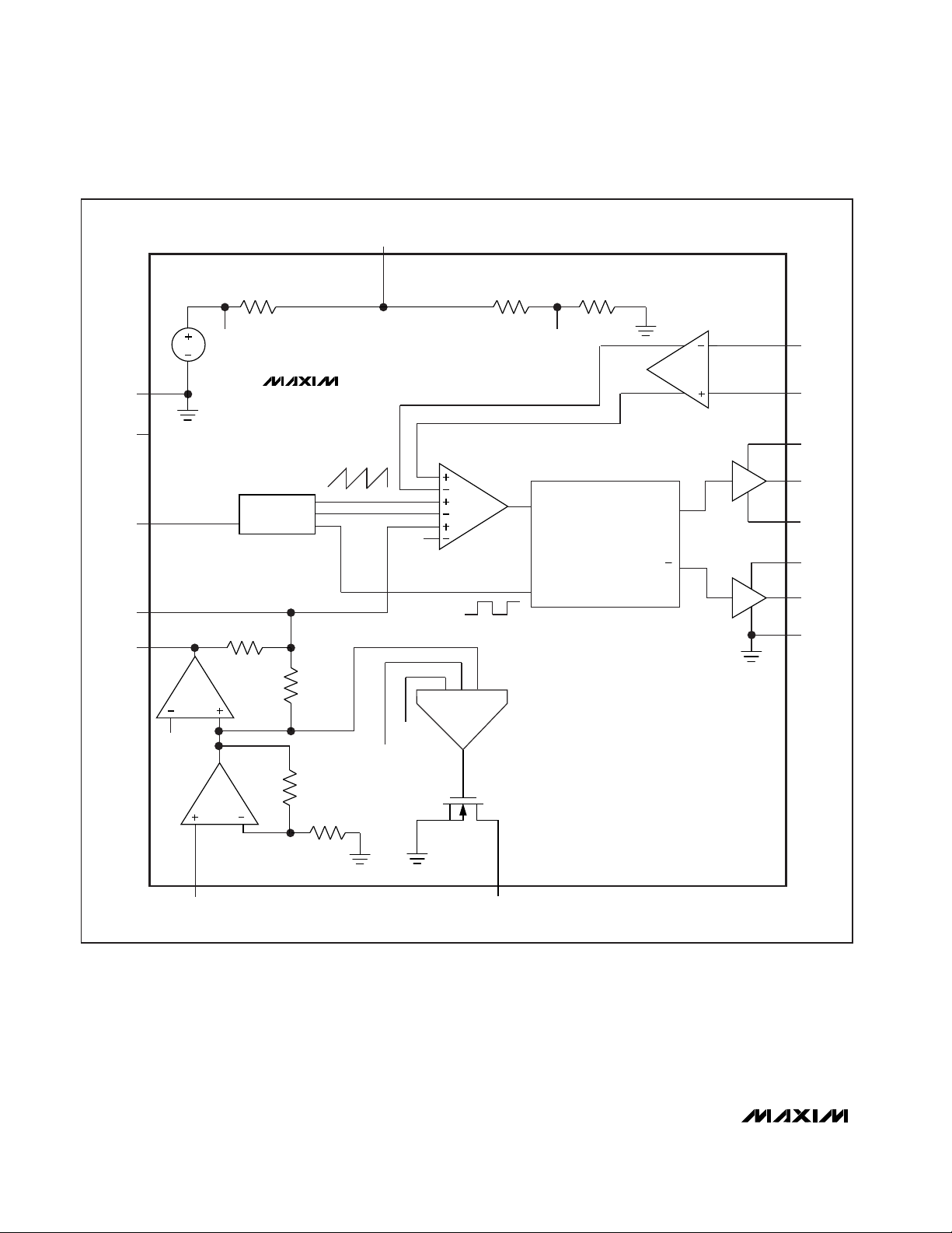
PWM Controller Block and Integrator
The heart of the current-mode PWM controller is a
multi-input, open-loop comparator that sums three signals (Figure 2): the buffered feedback signal, the current-sense signal, and the slope-compensation ramp.
This direct-summing configuration approaches ideal
cycle-by-cycle control over the output voltage. The output voltage error signal is generated by an error amplifier that compares the amplified feedback voltage to an
internal reference.
Each pulse from the oscillator sets the main PWM latch
that turns on the high-side switch for a period determined by the duty factor (approximately V
OUT
/ VIN). The
current-mode feedback system regulates the peak
inductor current as a function of the output voltage error
signal. Since average inductor current is nearly the same
as peak current (assuming the inductor value is set relatively high to minimize ripple current), the circuit acts as
a switch-mode transconductance amplifier. It pushes the
second output LC filter pole, normally found in a dutyfactor-controlled (voltage-mode) PWM, to a higher frequency. To preserve inner-loop stability and eliminate
regenerative inductor current staircasing, a slopecompensation ramp is summed into the main PWM comparator. Under fault conditions where the inductor current exceeds the maximum current-limit threshold, the
high-side latch resets, and the high-side switch turns off.
Internal Reference
The internal 3.5V reference (REF) is accurate to ±1%
from 0°C to +85°C, making REF useful as a system reference. Bypass REF to AGND with a 0.1µF (min)
ceramic capacitor. A larger value (such as 2.2µF) is
recommended for high-current applications. Load regulation is 10mV for loads up to 100µA. Reference
undervoltage lockout is between 2.7V and 3V. Shortcircuit current is less than 4mA.
Synchronous-Rectifier Driver
Synchronous rectification reduces conduction losses in
the rectifier by shunting the normal Schottky diode or
MOSFET body diode with a low-on-resistance MOSFET
switch. The synchronous rectifier also ensures proper
start-up by precharging the boost-charge pump used
for the high-side switch gate-drive circuit. Thus, if you
must omit the synchronous power MOSFET for cost or
other reasons, replace it with a small-signal MOSFET,
such as a 2N7002.
The DL drive waveform is simply the complement of the
DH high-side drive waveform (with typical controlled
dead time of 30ns to prevent cross-conduction or
shoot-through). The DL output’s on-resistance is 0.7Ω
(typ) and 2Ω (max).
10.0kΩ, 1%
10.0kΩ, 1%
R7
6.19kΩ, 1%
12.7kΩ, 1%
R8
Page 8
MAX1639
High-Speed Step-Down Controller with
Synchronous Rectification for CPU Power
8 _______________________________________________________________________________________
+
-
REF
REF2
REF
FB PWROK
CC2
CC1
REF1
24R
11R
N
10k
40k
WINDOW
CONTROL AND
DRIVE LOGIC
OSCILLATOR
SLOPE
COMPENSATION
AGND
V
CC
FREQ
REF1
REF
REF2
CSL
CSH
BST
DH
LX
V
DD
DL
RESET
Q
Q
SET
PGND
MAX1639
gm
Figure 2. Simplified Block Diagram
Page 9

MAX1639
High-Speed Step-Down Controller with
Synchronous Rectification for CPU Power
_______________________________________________________________________________________ 9
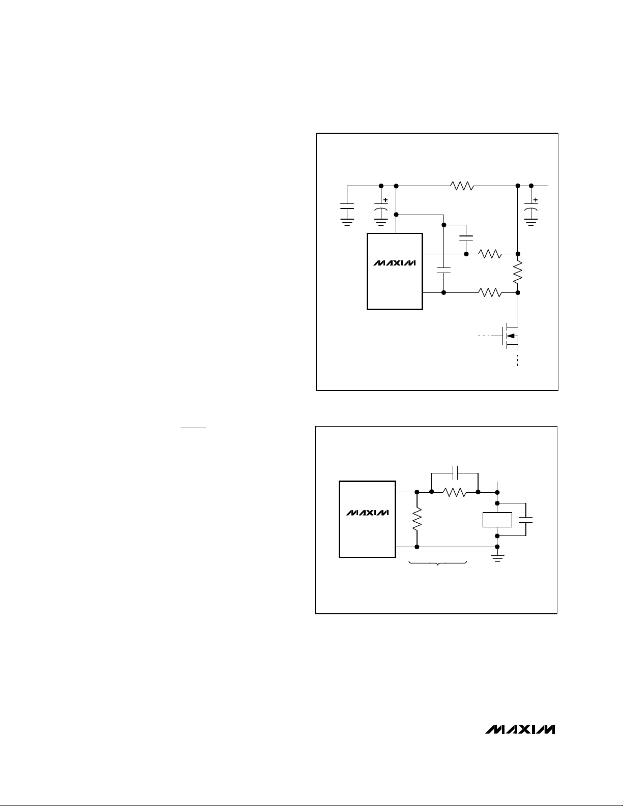
BST High-Side Gate-Driver Supply
and MOSFET Drivers
Gate-drive voltage for the high-side N-channel switch
is generated using a flying-capacitor boost circuit
(Figure 3). The capacitor is alternately charged from
the +5V supply and placed in parallel with the highside MOSFET’s gate and source terminals.
Gate-drive resistors (R3 and R4) can often be useful to
reduce jitter in the switching waveforms by slowing
down the fast-slewing LX node and reducing ground
bounce at the controller IC. However, switching loss
may increase. Low-value resistors from around 1Ω to
5Ω are sufficient for many applications.
Current Sense
and Overload Current Limiting
The current-sense circuit resets the main PWM latch
and turns off the high-side MOSFET switch whenever
the voltage difference between CSH and CSL from current through the sense resistor (R1) exceeds the peak
current limit (100mV typical).
Current-mode control provides cycle-by-cycle currentlimit capability for maximum overload protection.
During normal operation, the peak current limit set by
the current-sense resistor determines the maximum
output current. When the output is shorted, the peak
current may be higher than the set current limit due to
delays in the current-sense comparator. Thus, foldback
current limiting is employed where the set current-limit
point is reduced from 100mV to 38mV as the output
(feedback) voltage falls (Figure 4). When the shortcircuit condition is removed, the feedback voltage will
rise and the current-limit voltage will revert to 100mV.
The foldback current-limit circuit is designed to ensure
startup into a resistive load.
High-Side Current Sensing
The common-mode input range of the current-sense
inputs (CSH and CSL) extends to VCC, so it is possible
to configure the circuit with the current-sense resistor
on the input side rather than on the load side (Figure 5).
This configuration improves efficiency by reducing the
power dissipation in the sense resistor according to the
duty ratio.
In the high-side configuration, if the output is shorted
directly to GND through a low-resistance path, the
current-sense comparator may be unable to enforce a
current limit. Under such conditions, circuit parasitics
such as MOSFET R
DS(ON)
typically limit the shortcircuit current to a value around the peak-currentlimit setting.
Attach a lowpass-filter network between the currentsense pins and resistor to reduce high-frequency
common-mode noise. The filter should be designed
with a time constant of around one-fifth of the on-time
(130ns at 600kHz, for example). Resistors in the 20Ω to
100Ω range are recommended for R9 and R10.
Connect the filter capacitors C9 and C10 from V
CC
to
CSH and CSL, respectively.
Values of 39Ω and 3.3nF are suitable for many
designs. Place the current-sense filter network close to
the IC, within 0.1 in (2.5mm) of the CSH and CSL pins.
C3
C1
L1
D2
V
IN
= 5V
V
DD
N1
R4
DH
LEVEL
TRANSLATOR
CONTROL AND
DRIVE LOGIC
N2
R3
PGND
R3 AND R4
ARE OPTIONAL
LX
DL
BST
MAX1639
Figure 3. Boost Supply for Gate Drivers
0
20
10
50
40
30
60
70
100
90
80
20 30100 40 50 60 70 80 90 100
V
FB
(%)
I
LIM
(%)
Figure 4. Foldback Current Limit
Page 10
Overvoltage Protection
When the output exceeds the set voltage, the synchronous rectifier output (DL) is driven high (and DH is driven low). This causes the inductor to quickly dissipate
any stored energy and force the fault current to flow to
ground. Current is limited by the source impedance
and parasitic resistance of the current path, so a fuse is
required in series with the +5V input to protect against
low-impedance faults, such as a shorted high-side
MOSFET. Otherwise, the low-side MOSFET will eventually fail. DL will go low if the input voltage drops below
the undervoltage lockout point.
Internal Soft-Start
Soft-start allows a gradual increase of the internal current limit at start-up to reduce input surge currents. An
internal DAC raises the current-limit threshold from 0V
to 100mV in four steps (25mV, 50mV, 75mV, and
100mV) over the span of 1536 oscillator cycles.
__________________Design Procedure
Setting the Output Voltage
Set the output voltage by connecting R7 and R8 (Figure 6)
to the FB pin from the output to AGND. R7 is given by the
following equation:
where VFB= 1.1V. Since the input bias current at FB
has a maximum value of ±0.1µA, values up to 10kΩ
can be used for R8 with no significant accuracy loss.
Values under 1kΩ are recommended to improve noise
immunity. Place R7 and R8 very close to the MAX1639,
within 0.2in (5mm) of the FB pin.
Feed-Forward Compensation
An optional compensation capacitor (C8), typically
220pF, may be needed across the upper feedback
resistor to counter the effects of stray capacitance on the
FB pin, and to help ensure stable operation when highvalue feedback resistors are used (Figure 6). Empirically
adjust the feed-forward capacitor as needed.
Specifying the Inductor
Three key inductor parameters must be specified:
inductance value (L), peak current (I
PEAK
), and DC
resistance (RDC). The following equation includes a
constant LIR, which is the ratio of inductor peak-topeak AC current to DC load current. Typically LIR can
be between 0.1 to 0.5. A higher LIR value allows for
smaller inductors and better transient response, but
results in higher losses and output ripple. A good compromise between size and loss is a 30% ripple current
to load current ratio (LIR = 0.30), which corresponds to
a peak inductor current 1.15 times higher than the DC
load current.
R R x
V
V
OUT
FB
7 8 1 = −
MAX1639
High-Speed Step-Down Controller with
Synchronous Rectification for CPU Power
10 ______________________________________________________________________________________
C10
4.7nF
R1
C9
4.7nF
R9
39Ω
R5
10Ω
R10
39Ω
CSH
V
CC
CSL
MAX1639
N1
C5
0.1µFC610µF
C1
V
IN
Figure 5. High-Side Current Sense
R8
PLACE VERY CLOSE
TO MAX1639
R7
FB
AGND
V
OUT
C8 (OPTIONAL)
LOAD
MAX1639
Figure 6. Output Selection
Page 11

MAX1639
High-Speed Step-Down Controller with
Synchronous Rectification for CPU Power
______________________________________________________________________________________ 11
where f is the switching frequency, between 300kHz
and 1MHz; I
OUT
is the maximum DC load current; and
LIR is the ratio of AC to DC inductor current (typically
0.3). The exact inductor value is not critical and can be
adjusted to make trade-offs among size, transient
response, cost, and efficiency. Although lower inductor
values minimize size and cost, they also reduce efficiency due to higher peak currents. In general, higher
inductor values increase efficiency, but at some point
resistive losses due to extra turns of wire exceed the
benefit gained from lower AC current levels. Loadtransient response can be adversely affected by
high inductor values, especially at low (VIN- V
OUT
)
differentials.
The peak inductor current at full load is 1.15 x I
OUT
if
the previous equation is used; otherwise, the peak current can be calculated using the following equation:
The inductor’s DC resistance is a key parameter for efficient performance, and should be less than the currentsense resistor value.
Calculating the Current-Sense
Resistor Value
Calculate the current-sense resistor value according to
the worst-case minimum current-limit threshold voltage
(from the
Electrical Characteristics
) and the peak
inductor current required to service the maximum load.
Use I
PEAK
from the equation in the section
Specifying
the Inductor
.
The high inductance of standard wire-wound resistors
can degrade performance. Low-inductance resistors,
such as surface-mount power metal-strip resistors, are
preferred. The current-sense resistor’s power rating
should be higher than the following:
In high-current applications, connect several resistors
in parallel as necessary to obtain the desired resistance and power rating.
Selecting the Output Filter Capacitor
Output filter capacitor values are generally determined
by effective series resistance (ESR) and voltage-rating
requirements, rather than by the actual capacitance
value required for loop stability. Due to the high switching currents and demanding regulation requirements in
a typical MAX1639 application, use only specialized
low-ESR capacitors intended for switchingregulator applications, such as AVX TPS, Kemet T510,
Sprague 595D, Sanyo OS-CON, or Sanyo GX series. Do
not use standard aluminum-electrolytic capacitors,
which can cause high output ripple and instability due
to high ESR. The output voltage ripple is usually dominated by the filter capacitor’s ESR, and can be approximated as I
RIPPLE
x R
ESR
. To ensure stability, the
capacitor must meet
both
minimum capacitance and
maximum ESR values as given in the following equations:
Compensating the Feedback Loop
The feedback loop needs proper compensation to prevent excessive output ripple and poor efficiency
caused by instability. Compensation cancels unwanted
poles and zeros in the DC-DC converter’s transfer function that are due to the power-switching and filter elements with corresponding zeros and poles in the
feedback network. These compensation zeros and
poles are set by the compensation components CC1,
CC2, and RC1. The objective of compensation is to
ensure stability by ensuring that the DC-DC converter’s
phase shift is less than 180° by a safe margin, at the
frequency where the loop gain falls below unity.
Canceling the Sampling Pole
and Output Filter ESR Zero
Compensate the fast-voltage feedback loop by connecting a resistor and a capacitor in series from the
CC1 pin to AGND. The pole from CC1 can be set to
cancel the zero from the filter-capacitor ESR. Thus the
capacitor at CC1 should be as follows:
C
V
V
V
V x R x f
R R
OUT
REF
OUT
IN MIN
OUT SENSE OSC
ESR SENSE
( )
>
+
<
1
I x R
OUT MAX SENSE( )
2
R
mV
I
SENSE
PEAK
=
85
I I
V V V
f x L x V
PEAK OUT
OUT INMAX OUT
OSC IN MAX
( )
( )
= +
−
( )
2
L
V V V
V x f x I x LIR
OUT INMAX OUT
IN MAX OSC OUT
( )
( )
=
−
( )
Page 12

MAX1639
High-Speed Step-Down Controller with
Synchronous Rectification for CPU Power
12 ______________________________________________________________________________________
Resistor RC1 sets a zero that can be used to compensate for the sampling pole generated by the switching
frequency. Set RC1 to the following:
The CC1 pin’s output resistance is 10kΩ.
Setting the Dominant Pole
and Canceling the Load and Output Filter Pole
Compensate the slow-voltage feedback loop by adding
a ceramic capacitor from the CC2 pin to AGND. This is
an integrator loop used to cancel out the DC loadregulation error. Selection of capacitor CC2 sets the
dominant pole and a compensation zero. The zero is typically used to cancel the unwanted pole generated by the
load and output filter capacitor at the maximum load current. Select CC2 to place the zero close to or slightly
lower than the frequency of the unwanted pole, as follows:
The transconductance of the integrator amplifier at CC2
is 1mmho. The voltage swing at CC2 is internally
clamped around 2.4V to 3V minimum and 4V to V
CC
maximum to improve transient response times. CC2
can source and sink up to 100µA.
Choosing the MOSFET Switches
The two high-current N-channel MOSFETs must be
logic-level types with guaranteed on-resistance specifications at VGS= 4.5V. Lower gate-threshold specs are
better (i.e., 2V max rather than 3V max). Gate charge
should be less than 200nC to minimize switching losses
and reduce power dissipation.
I2R losses are the greatest heat contributor to MOSFET
power dissipation and are distributed between the
high- and low-side MOSFETs according to duty factor,
as follows:
Gate-charge losses are dissipated in the IC, and do not
heat the MOSFETs. Ensure that both MOSFETs are at a
safe junction temperature by calculating the temperature
rise according to package thermal-resistance specifications. The high-side MOSFET’s worst-case dissipation
occurs at the maximum output voltage and minimum
input voltage. For the low-side MOSFET, the worst case
is at the maximum input voltage when the output is shortcircuited (consider the duty factor to be 100%).
Calculating IC Power Dissipation
Power dissipation in the IC is dominated by average
gate-charge current into both MOSFETs. Average current is approximately:
IDD= (QG1+ QG2) x f
OSC
where IDDis the drive current, QGis the total gate
charge for each MOSFET, and f
OSC
is the switching
frequency.
Power dissipation of the IC is:
PD= ICCx VCC+ IDDx V
DD
where ICCis the quiescent supply current of the IC.
Junction temperature for the IC is primarily a function of
the PC board layout, since most of the heat is removed
through the traces connected to the pins and the
ground and power planes. A 16-pin narrow SO on a
typical four-layer board with ground and power planes
show equivalent junction-to-ambient thermal
impedance of (θJA) about 80°C/W. Junction temperature of the die is approximately:
TJ= PDx θJA+ T
A
where TAis the ambient temperature.
Selecting the Rectifier Diode
The rectifier diode D1 is a clamp that catches the negative inductor swing during the 30ns typical dead time
between turning off the high-side MOSFET and turning
on the low-side MOSFET synchronous rectifier. D1 must
be a Schottky diode, to prevent the MOSFET body
diode from conducting. It is acceptable to omit D1 and
let the body diode clamp the negative inductor swing,
but efficiency will drop about 1%. Use a 1N5819 diode
for loads up to 3A, or a 1N5822 for loads up to 10A.
Adding the BST Supply Diode
and Capacitor
A signal diode, such as a 1N4148, works well for D2 in
most applications, although a low-leakage Schottky
diode provides slightly improved efficiency. Do not use
P low side I x R x
V
V
D LOAD DS ON
OUT
IN
( )
( )
= −
2
1
P high side I x R x
V
V
D LOAD DS ON
OUT
IN
( )
( )
=
2
CC
mmho x C
x
V
I
OUT OUT
OUT MAX
2
1
4
( )
=
RC
V
V
f x CC
OUT
IN
OSC
1
1
2 1
=
+
CC
C x R
k
OUT ESR
110
=Ω
Page 13
MAX1639
High-Speed Step-Down Controller with
Synchronous Rectification for CPU Power
______________________________________________________________________________________ 13
large power diodes, such as the 1N4001 or 1N5817.
Exercise caution in the selection of Schottky diodes,
since some types exhibit high reverse leakage at high
operating temperatures. Bypass BST to LX using a
0.1µF capacitor.
Selecting the Input Capacitors
Place a 0.1µF ceramic capacitor and 10µF capacitor
between VCCand AGND, as well as between VDDand
PGND, within 0.2 in. (5mm) of the VCCand VDDpins.
Select low-ESR input filter capacitors with a ripplecurrent rating exceeding the RMS input ripple current,
connecting several capacitors in parallel if necessary.
RMS input ripple current is determined by the input
voltage and load current, with the worst-possible case
occurring at VIN= 2 x V
OUT
:
__________Applications Information
Efficiency Considerations
Refer to the MAX796–MAX799 data sheet for information on calculating losses and improving efficiency.
PC Board Layout Considerations
Good PC board layout and routing are
required
in highcurrent, high-frequency switching power supplies to
achieve good regulation, high efficiency, and stability.
The PC board layout artist must be provided with explicit
instructions concerning the placement of power-switching components and high-current routing. It is strongly
recommended that the evaluation kit PC board layouts
be followed as closely as possible. Contact Maxim’s
Applications Department concerning the availability of
PC board examples for higher-current circuits.
In most applications, the circuit is on a multilayer
board, and full use of the four or more copper layers is
recommended. Use the top layer for high-current
power and ground connections. Leave the extra copper on the board as a pseudo-ground plane. Use the
bottom layer for quiet connections (REF, FB, AGND),
and the inner layers for an uninterrupted ground plane.
A ground plane and pseudo-ground plane are essential
for reducing ground bounce and switching noise.
Place the high-power components (C1, R1, N1, D1, N2,
L1, and C2 in Figure 1) as close together as possible.
Minimize ground-trace lengths in high-current paths.
The surface-mount power components should be
butted up to one another with their ground terminals
almost touching. Connect their ground terminals using
a wide, filled zone of top-layer copper (the pseudoground plane), rather than through the internal ground
plane. At the output terminal, use vias to connect the
top-layer pseudo-ground plane to the normal innerlayer ground plane at the output filter capacitor ground
terminals. This minimizes interference from IR drops
and ground noise, and ensures that the IC’s AGND is
sensing at the supply’s output terminals.
Minimize high-current path trace lengths. Use very
short and wide traces. From C1 to N1: 0.4 in. (10mm)
max length; D1 anode to N2: 0.2 in. (5mm) max length;
LX node (N1 source, N2 drain, D1 cathode, inductor
L1): 0.6 in. (15mm) max length.
I I
V V V
V
I I when V V
RMS LOAD MAX
OUT IN OUT
IN
RMS OUT IN OUT
( )
/
( )
=
−
= =2 2
___________________Pin Configuration
___________________Chip Information
16
15
14
13
12
11
10
9
1
2
3
4
5
6
7
8
BST DH
LX
PGND
DL
V
DD
FREQ
CC2
CC1
TOP VIEW
MAX1639
16 SOIC
PWROK
CSL
REF
CSH
V
CC
AGND
FB
TRANSISTOR COUNT: 3135
SUBSTRATE CONNECTED TO AGND
 Loading...