

Page 1
For free samples & the latest literature: http://www.maxim-ic.com, or phone 1-800-998-8800.
For small orders, phone 408-737-7600 ext. 3468.
General Description
The MAX1637 synchronous, buck, switch-mode powersupply controller generates the CPU supply voltage in
battery-powered systems. The MAX1637 is a strippeddown version of the MAX1636 in a smaller 16-pin QSOP
package. The MAX1637 is intended to be powered separately from the battery by an external bias supply (typically the +5V system supply) in applications where the
battery exceeds 5.5V. The MAX1637 achieves excellent
DC and AC output voltage accuracy. This device can
operate from a low input voltage (3.15V) and delivers the
excellent load-transient response needed by upcoming
generations of dynamic-clock CPUs.
Using synchronous rectification, the MAX1637 achieves
up to 95% efficiency. Efficiency is greater than 80%
over a 1000:1 load-current range, which extends battery life in system-suspend or standby mode. Excellent
dynamic response corrects output load transients
caused by the latest dynamic-clock CPUs within five
300kHz clock cycles. Powerful 1A on-board gate driversensure fast external N-channel MOSFET switching.
The MAX1637 features a logic-controlled and synchronizable, fixed-frequency, pulse-width-modulation
(PWM) operating mode. This reduces noise and RF
interference in sensitive mobile-communications and
pen-entry applications. Asserting the SKIP pin enables
fixed-frequency mode, for lowest noise under all load
conditions. For a stand-alone device that includes a
+5V VL linear regulator and low-dropout capabilities,
refer to the MAX1636 data sheet.
________________________Applications
Notebook Computers Subnotebook Computers
Handy-Terminals, PDAs
____________________________Features
♦ ±2% DC Accuracy
♦ 0.1% (typ) DC Load Regulation
♦ Adjustable Switching Frequency to 350kHz
♦ Idle Mode™ Pulse-Skipping Operation
♦ 1.10V to 5.5V Adjustable Output Voltage
♦ 3.15V Minimum IC Supply Voltage (at V
CC
pin)
♦ Internal Digital Soft-Start
♦ 1.1V ±2% Reference Output
♦ 1µA Total Shutdown Current
♦ Output Overvoltage Crowbar Protection
♦ Output Undervoltage Shutdown (foldback)
♦ Tiny 16-Pin QSOP Package
MAX1637
Miniature, Low-Voltage,
Precision Step-Down Controller
________________________________________________________________
Maxim Integrated Products
1
16
15
14
13
12
11
10
9
1
2
3
4
5
6
7
8
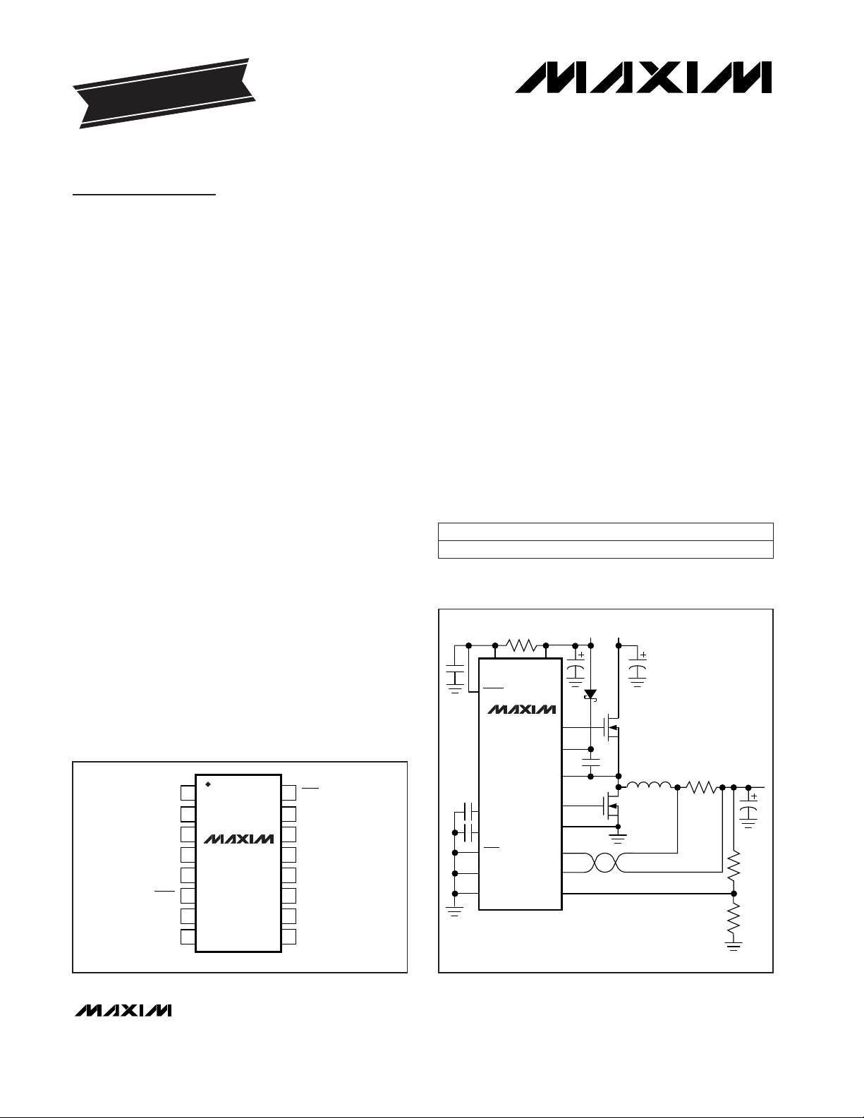
CSH SKIP
LX
DH
BST
PGND
DL
V
GG
V
CC
TOP VIEW
MAX1637
QSOP
CSL
FB
SHDN
CC
REF
SYNC
GND
__________________Pin Configuration
__________Typical Operating Circuit
19-1321; Rev 1; 2/98
PART
MAX1637EEE -40°C to +85°C
TEMP. RANGE PIN-PACKAGE
16 QSOP
EVALUATION KIT
AVAILABLE
______________Ordering Information
Idle Mode is a trademark of Maxim Integrated Products.
MAX1637
SHDN
GND
V
BATT
V
BIAS
DL
PGND
LX
DH
V
CC
V
GG
BST
CSH
CSL
FB
SKIP
SYNC
REF
CC
OUTPUT
Page 2
MAX1637
Miniature, Low-Voltage,
Precision Step-Down Controller
2 _______________________________________________________________________________________
ABSOLUTE MAXIMUM RATINGS
ELECTRICAL CHARACTERISTICS
(Circuit of Figure 1, VCC= VGG= 5V, SYNC = VCC, I
REF
= 0mA, TA= 0°C to +85°C, unless otherwise noted. Typical values are at
T
A
= +25°C.)
Stresses beyond those listed under “Absolute Maximum Ratings” may cause permanent damage to the device. These are stress ratings only, and functional
operation of the device at these or any other conditions beyond those indicated in the operational sections of the specifications is not implied. Exposure to
absolute maximum rating conditions for extended periods may affect device reliability.
GND to PGND .............................................................+2V to -2V
LX, BST to GND......................................................-0.3V to +36V
BST, DH to LX...........................................................-0.3V to +6V
V
CC
, VGG, CSL, CSH, SHDN to GND.......................-0.3V to +6V
DL to GND..................................................-0.3V to (V
GG
+ 0.3V)
REF, SKIP, SYNC, CC to GND ...................-0.3V to (V
CC
+ 0.3V)
REF Output Current.............................................................20mA
REF Short-Circuit to GND..............................................Indefinite
Operating Temperature Range ...........................-40°C to +85°C
Continuous Power Dissipation (T
A
= +70°C)
QSOP (derate 8.3mW/°C above +70°C)......................667mW
Storage Temperature Range.............................-65°C to +160°C
Junction Temperature......................................................+150°C
Lead Temperature (soldering, 10sec).............................+300°C
SYNC = GND
SYNC = V
CC
FB tied to V
OUT
, 0mV < (CSH - CSL) < 80mV,
includes line and load regulation
VCC= 3.15V to 5.5V
REF load = 0µA to 50µA
VCC, V
GG
REF load = 0µA
Rising edge, hysteresis = 15mV
Rising edge, hysteresis = 15mV
SHDN = GND, VCC= V
GG
CSH - CSL = 0mV to CSH - CSL = 100mV
CSH - CSL
VCC= 5V
VCC= 3.3V
SHDN to full current limit, four levels
VFB= V
REF
CONDITIONS
170 200 230
Oscillator Frequency kHz
270 300 330
mV3REF Line Regulation
mV10REF Load Regulation
V1.080 1.100 1.120REF Output Voltage
V2.80 3.05VGGUndervoltage Lockout Threshold
V2.80 3.05VCCUndervoltage Lockout Threshold
%2AC Load Regulation
mV20 30 40Idle-Mode Switchover Threshold
clocks512Soft-Start Ramp Time
nA-50 50FB Input Current
V3.15 5.5Input Voltage Range
µA0.5 3Shutdown Supply Current
V1.080 1.100 1.120Output Voltage
V
REF
5.5
Output Adjustment Range V
V
REF
3.6
UNITSMIN TYP MAXPARAMETER
CSH > CSL
CSH < CSL
80 100 120
Current-Limit Threshold mV
-145 -100 -55
Output not switching
1.5 2.5
Power Consumption mW
1 1.75
SYNC = GND
SYNC = V
CC
ns200SYNC Input Pulse Width High
%
93 96
89 92
Maximum Duty Factor
(Note 1)
kHz240 340SYNC Input Frequency Range
ns200SYNC Input Rise/Fall Time
ns200SYNC Input Pulse Width Low
VCC= VGG= 5V
VCC= VGG= 3.3V
SMPS CONTROLLER
INTERNAL REFERENCE
OSCILLATOR
Page 3
MAX1637
Miniature, Low-Voltage,
Precision Step-Down Controller
_______________________________________________________________________________________ 3
ELECTRICAL CHARACTERISTICS (continued)
(Circuit of Figure 1, VCC= VGG= 5V, SYNC = VCC, I
REF
= 0mA, TA= 0°C to +85°C, unless otherwise noted. Typical values are at
T
A
= +25°C.)
ELECTRICAL CHARACTERISTICS
(Circuit of Figure 1, VCC= VGG= 5V, SYNC = VCC, I
REF
= 0mA, TA= -40°C to +85°C, unless otherwise noted.) (Note 2)
High or low, DH or DL
DH or DL forced to 2V
CSH = CSL = 5V, VCC= VGG= GND,
either CSH or CSL input
FB to DL delay, 22mV overdrive, C
GATE
= 2000pF
FB, with respect to regulation point
From shutdown or power-on-reset state
Pin at GND or V
CC
SHDN, SKIP, SYNC
% of nominal output
SHDN, SKIP, SYNC
CONDITIONS
Ω7Gate Driver On-Resistance
A1Gate Driver Sink/Source Current
µA10Current-Sense Input Leakage Current
µA-1 1Logic Input Bias Current
V0.8Logic Input Voltage Low
V2.4Logic Input Voltage High
µs1.25Overvoltage Fault Propagation Delay
%4 7 10Overvoltage Trip Threshold
clocks6144Output Undervoltage Lockout Delay
%60 70 80Output Undervoltage Lockout Threshold
UNITSMIN TYP MAXPARAMETER
FB tied to V
OUT
, 0mV < (CSH - CSL) < 80mV,
includes line and load regulation
SYNC = GND
VCC, V
GG
SYNC = V
CC
Rising edge, hysteresis = 15mV
Rising edge, hysteresis = 15mV
VCC= 3.3V
VCC= VGG= 3.3V, output not switching
VCC= 5V
VCC= VGG= 5V, output not switching
CSH > CSL
CONDITIONS
kHz240 340SYNC Input Frequency Range
ns200SYNC Input Rise/Fall Time
ns200SYNC Input Pulse Width Low
ns200SYNC Input Pulse Width High
kHz
170 230
Oscillator Frequency
262 338
V2.80 3.05VGGUndervoltage Lockout Threshold
V2.80 3.05VCCUndervoltage Lockout Threshold
mW1.75
Power Consumption
mW2.5
mV70 130Current-Limit Threshold
V1.080 1.120Output Voltage
V3.15 5.5Input Voltage Range
V
REF
3.6
Output Adjustment Range V
V
REF
5.5
UNITSMIN TYP MAXPARAMETER
OVERVOLTAGE PROTECTION
INPUTS AND OUTPUTS
SMPS CONTROLLER
INTERNAL REFERENCE
OSCILLATOR
Page 4
0
10
5
15
20
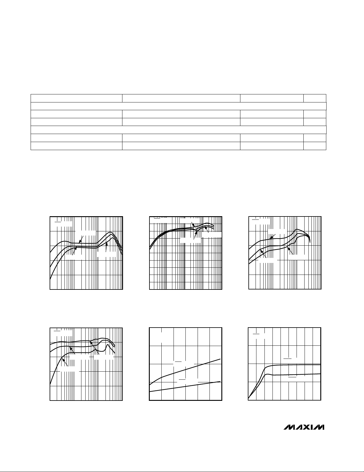
0 3 41 2 5 6 87 9
SUPPLY CURRENT
vs. LOAD CURRENT
MAX1637-07
LOAD CURRENT (A)
V
CC
+ V
GG
SUPPLY CURRENT (mA)
SYNC = HIGH
SYNC = LOW
SKIP = LOW
MAX1637
Miniature, Low-Voltage,
Precision Step-Down Controller
4 _______________________________________________________________________________________
ELECTRICAL CHARACTERISTICS (continued)
(Circuit of Figure 1, VCC= VGG= 5V, SYNC = VCC, I
REF
= 0mA, TA= -40°C to +85°C, unless otherwise noted.) (Note 2)
SHDN, SKIP, SYNC
SHDN, SKIP, SYNC
% of nominal output
FB, with respect to regulation point
CONDITIONS
V0.8Logic Input Voltage Low
V2.4Logic Input Voltage High
%60 80Output Undervoltage Lockout Threshold
%4.0 10Overvoltage Trip Threshold
UNITSMIN TYP MAXPARAMETER
Note 1: Guaranteed by design, not production tested.
Note 2: Specifications from -40°C to 0°C are guaranteed by design and not production tested.
__________________________________________Typical Operating Characteristics
(V
OUT
= 3.3V, TA = +25°C, unless otherwise noted.)
100
50
0.01 1010.1
EFFICIENCY vs. LOAD CURRENT
(1.7V/7A CIRCUIT)
70
60
90
80
MAX1637-01
LOAD CURRENT (A)
EFFICIENCY (%)
SKIP = LOW
V
BATT
= 7V
V
BATT
= 15V
V
BATT
= 22V
100
0
0.001 1010.01 0.1
EFFICIENCY vs. LOAD CURRENT
(2.5V/3A CIRCUIT)
40
30
20
10
80
70
90
60
50
MAX1637-02
LOAD CURRENT (A)
EFFICIENCY (%)
V
BATT
= 15V
SKIP = LOW
V
BATT
= 7V
V
BATT
= 22V
100
50
0.01 1010.1
EFFICIENCY vs. LOAD CURRENT
(2.5V/2A CIRCUIT)
70
60
90
80
MAX1637-03
LOAD CURRENT (A)
EFFICIENCY (%)
V
BATT
= 7V
SKIP = LOW
V
BATT
= 15V
V
BATT
= 22V
100
50
0.01 1010.1
EFFICIENCY vs. LOAD CURRENT
(3.3V/3A CIRCUIT)
70
60
90
80
MAX1637-04
LOAD CURRENT (A)
EFFICIENCY (%)
V
BATT
= 5V
V
BATT
= 30V
V
BATT
= 15V
SKIP = LOW
0
10
5
15
20
3.0 4.03.5 4.5 5.0
5.5
6.0
SUPPLY CURRENT
vs. SUPPLY VOLTAGE
MAX1637-06
SUPPLY VOLTAGE (V)
V
CC
+ V
GG
SUPPLY CURRENT (mA)
I
LOAD
= 1A
V
OUT
= 3.3V
SKIP = HIGH
SKIP = LOW
OVERVOLTAGE PROTECTION
INPUTS AND OUTPUTS
Page 5
MAX1637
Miniature, Low-Voltage,
Precision Step-Down Controller
_______________________________________________________________________________________
5
10
-10
0.01 1010.1
LOAD REGULATION
vs. LOAD CURRENT
-2
-6
-8
6
8
4
0
-4
2
MAX1637-08
LOAD CURRENT (A)
LOAD REGULATION ∆V
OUT
(mV)
0
0.3
0.2
0.1
0.4
0.5
0.6
0 403010 20 50 60 70 80 90 100
REF LOAD-REGULATION ERROR
vs. REF LOAD CURRENT
MAX1637-09
REF LOAD CURRENT (µA)
REF LOAD REGULATION ∆V (mV)
900
0
0.01 1010.1
DROPOUT VOLTAGE
vs. LOAD CURRENT
300
200
100
700
800
600
400
500
MAX1637-10
LOAD CURRENT (A)
DROPOUT VOLTAGE (mV)
V
OUT
FORCED TO 3.27V
SYNC = V
CC
V
OUT
20mV/div
V
LX
INDUCTOR
CURRENT
1A
0V
5V
0A
SWITCHING WAVEFORMS
(PWM MODE)
MAX1637-13
1µs/div
V
OUT
50mV/div
LOAD
CURRENT
0A
2A
4A
LOAD-TRANSIENT RESPONSE
(3.3V/3A, PWM MODE)
MAX1637 TOC11
100µs/div
V
OUT
50mV/div
5A LOAD CURRENT
0A
10A
LOAD-TRANSIENT RESPONSE
(1.8V, PWM MODE)
MAX1637 TOC12
100µs/div
V
OUT
50mV/div
V
LX
INDUCTOR
CURRENT
1A
0V
5V
0A
SWITCHING WAVEFORMS
(PFM MODE)
MAX1637-14
20µs/div
V
OUT
= 1.7V
1µs/div
SWITCHING WAVEFORMS
DROPOUT OPERATION
MAX1637-15
V
OUT
10mV/div
V
LX
2V/div
INDUCTOR
CURRENT
1A
0A
V
OUT
FORCED TO 3.27V
SYNC = V
CC
____________________________________Typical Operating Characteristics (continued)
(V
OUT
= 3.3V, TA = +25°C, unless otherwise noted.)
Page 6
MAX1637
Miniature, Low-Voltage,
Precision Step-Down Controller
6 _______________________________________________________________________________________
____________________________________Typical Operating Characteristics (continued)
(V
OUT
= 3.3V, TA = +25°C, unless otherwise noted.)
500µs/div
TIME EXITING SHUTDOWN
(V
OUT
= 3.3V, I
LOAD
= 7A)
MAX1637-16
V
OUT
1V/div
V
SHDN
5V/div
V
OUT
100mV/div
V
DL
INDUCTOR
CURRENT
-5A
0A
0V
5V
-10A
OVERVOLTAGE-PROTECTION WAVEFORMS
(V
IN
SHORTED TO V
OUT
THROUGH A 0.5Ω RESISTOR)
MAX1637-17
10µs/div
______________________________________________________________Pin Description
PIN
High-Side Current-Sense InputCSH1
FUNCTIONNAME
Low-Side Current-Sense InputCSL2
Compensation Pin. Connect a small capacitor to GND to set the integration time constant.CC4
Feedback Input. Connect to center of resistor divider.FB3
Shutdown Control Input. Turns off entire IC. When low, reduces supply current below 0.5µA (typ). Drive with
logic input or connect to RC network between GND and VCCfor automatic start-up.
SHDN
6
Analog GroundGND8
Oscillator Frequency Select and Synchronization Input. Tie to VCCfor 300kHz operation; tie to GND for
200kHz operation.
SYNC7
1.100V Reference Output. Capable of sourcing 50µA for external loads. Bypass with 0.22µF minimum.REF5
Gate-Drive and Boost-Circuit Power Supply. Can be driven from a supply other than VCC. If the same supply
is used by both VCCand VGG, isolate VCCfrom VGGwith a 20Ω resistor. Bypass to PGND with a 4.7µF
capacitor. VGGcurrent = (QG1+ QG2) x f, where QGis the MOSFET gate charge at VGS= VGG.
V
GG
10
Power GroundPGND12
Low-Side Gate-Driver OutputDL11
High-Side Gate-Driver OutputDH14
Low-Noise Mode Control. Forces fixed-frequency PWM operation when high.
SKIP
16
Inductor ConnectionLX15
Boost Capacitor ConnectionBST13
Main Analog Supply-Voltage Input to the Chip. VCCpowers the PWM controller, logic, and reference. Input
range is 3.15V to 5.5V. Bypass to GND with a 0.1µF capacitor close to the pin.
V
CC
9
Page 7

MAX1637
Miniature, Low-Voltage,
Precision Step-Down Controller
_______________________________________________________________________________________ 7
MAX1637
0.1µF
V
BIAS
+5V
NOMINAL
0.1µF
1µF
470pF
C1
Q1
CMPSH-3
Q2
C2
L1
*
R1
R2
R3
OUTPUT
4.7µF
*SEE
RECTIFIER CLAMP DIODE
SECTION
**OPTIONAL RC NETWORK FOR POWER-ON-RESET
DL
PGND
LX
DH
BST
V
GG
V
CC
V
BATT
CSH
CSL
FB
1M
**
ON/OFF
CC
GND
SHDN
REF
SYNC
20Ω
SKIP
0.01µF**
Figure 1. Standard Application Circuit
______Standard Application Circuit
The basic MAX1637 buck converter (Figure 1) is easily
adapted to meet a wide range of applications where a
5V or lower supply is available. The components listed
in Table 1 represent a good set of trade-offs among
cost, size, and efficiency, while staying within the worstcase specification limits for stress-related parameters
such as capacitor ripple current. Do not change the circuit’s switching frequency without first recalculating
component values (particularly inductance value at
maximum battery voltage).
The power Schottky diode across the synchronous rectifier is optional because the MOSFETs chosen incorporate a high-speed silicon diode. However, installing the
Schottky will generally improve efficiency by about 1%.
If used, the Schottky diode DC current must be rated to
at least one-third of the maximum load current.
_______________Detailed Description
The MAX1637 is a BiCMOS, switch-mode power-supply
(SMPS) controller designed primarily for buck-topology
regulators in battery-powered applications where high
efficiency and low quiescent supply current are critical.
Light-load efficiency is enhanced by automatic idlemode operation—a variable-frequency, pulse-skipping
mode that reduces transition and gate-charge losses.
The step-down, power-switching circuit consists of two
N-channel MOSFETs, a rectifier, and an LC output filter.
Output voltage for this device is the average AC voltage at the switching node, which is regulated by
changing the duty cycle of the MOSFET switches. The
gate-drive signal to the high-side N-channel MOSFET,
which must exceed the battery voltage, is provided by
a flying-capacitor boost circuit that uses a 100nF
capacitor between BST and LX. Figure 2 shows the
major circuit blocks.
Page 8

LOAD CURRENT
MAX1637
Miniature, Low-Voltage,
Precision Step-Down Controller
8 _______________________________________________________________________________________
Table 1. Component Selection for Standard Applications
Table 2. Component Suppliers
2.5VOutput Voltage Range
300kHzFrequency
Chipset SupplyApplication
1/2 Si4902DY or
1/2 MMDF3NO3HD
Q1 High-Side
MOSFET
7V to 22VInput Voltage Range
(619) 661-6835(81) 7-2070-1174Sanyo
Tokin (408) 432-8020
(847) 390-4373
(1) 408-434-0375
(1) 847-390-4428TDK
Sprague
(847) 956-0666(81) 3-3607-5144Sumida
(603) 224-1961
(714) 373-7939
(408) 988-8000
(1) 714-373-7183Panasonic
(1) 603-224-1430
(1) 408-970-3950Siliconix
(602) 303-5454(1) 602-994-6430Motorola
(847) 696-2000
COMPANY
Matsuo (714) 969-2491(1) 714-960-6492
USA PHONE
FACTORY FAX
(COUNTRY CODE)
(1) 847-696-9278
Marcon/United
Chemi-Con
COMPANY
Central
Semiconductor
Fairchild (408) 721-2181(1) 408-721-1635
(512) 992-7900(1) 512-992-3377IRC
Dale
(310) 322-3331(1) 310-322-3332
International
Rectifier (IR)
(605) 668-4131
(847) 639-6400
(561) 241-7876
(1) 847-639-1469Coilcraft
(1) 605-665-1627
(1) 561-241-9339Coiltronics
USA PHONE
(516) 435-1110
(803) 946-0690
FACTORY FAX
(COUNTRY CODE)
(1) 516-435-1824
(1) 803-626-3123AVX
2.5V
300kHz
Chipset Supply
International Rectifier
IRF7403 or
Siliconix Si4412
7V to 22V
3.3V1.7V
300kHz300kHz
General PurposeCPU Core
International Rectifier
IRF7403 or
Siliconix Si4412
Fairchild FDS9412 or
International Rectifier
IRF7403
4.75V to 30V7V to 22V
10µF, 25V ceramic
Tokin C34Y5U1E106Z
or Marcon/United
Chemicon
THCR40E1E106ZT
10µF, 25V ceramic
Tokin C34Y5U1E106Z
or Marcon/United
Chemicon
THCR40E1E106ZT
C1 Input Capacitor
0.020Ω, 1% (2010)
Dale WSL-2010-R020F
0.033Ω, 1% (2010)
Dale WSL-2010-R033F
R1 Resistor
470µF, 6.3V tantalum
Kemet
T510X477(1)006AS or
470µF, 4V tantalum
Sprague
594D477X0004R2T
220µF, 6.3V tantalum
Sprague
595D227X96R3C2
C2 Output Capacitor
10µH
Sumida CDRH125-100
10µH
Coilcraft
DO3316P-103 or
Coiltronics UP2-100
L1 Inductor
International Rectifier
IRF7413 or
Siliconix Si4410DY
1/2 Si4902DY or
1/2 MMDF3NO3HD
Q2 Low-Side MOSFET
10µF, 30V
Sanyo OS-CON
4 x 10µF, 25V ceramic
Tokin C34Y5U1E106Z
or Marcon/United
Chemicon
THCR40E1E106ZT
0.020Ω, 1% (2010)
Dale WSL-2010-R020F
0.010Ω, 1% (2512)
Dale WSL-2512-R010F
470µF, 6.3V tantalum
Kemet
T510X477(1)006AS or
470µF, 4V tantalum
Sprague
594D477X0004R2T
3 x 470µF, 6.3V tantalum
Kemet
T510X477(1)006AS or
470µF, 4V tantalum
Sprague
594D477X0004R2T
10µH Sumida
CDRH125-100
2.2µH
Panasonic P1F2R0HL or
Coiltronics UP4-2R2 or
Coilcraft
DO5022P-222HC
International Rectifier
IRF7413 or
Siliconix Si4410DY
Fairchild FDS6680 or
Siliconix Si4420DY
COMPONENT
3A (EV KIT)2A 3A7A (EV KIT)
LOAD CURRENT
Page 9

MAX1637
Miniature, Low-Voltage,
Precision Step-Down Controller
_______________________________________________________________________________________ 9
The pulse-width-modulation (PWM) controller consists
of a multi-input PWM comparator, high-side and lowside gate drivers, and logic. It uses a 200kHz/300kHz
synchronizable oscillator. The MAX1637 contains faultprotection circuits that monitor the PWM output for
undervoltage and overvoltage. It includes a 1.100V pre-
cision reference. The circuit blocks are powered from
an internal IC power rail that receives power from VCC.
VGGprovides direct power to the synchronous-switch
gate driver, but provides indirect power to the highside-switch gate driver via an external diode-capacitor
boost circuit.
REF
IC
POWER
200kHz
TO
300kHz
OSC
PWM
LOGIC
3.15V TO 5.5V
V
BATT
V
OUT
REF
SHDN
SYNC
V
CC
DL
PGND
LX
DH
BST
V
GG
SKIP
CSH
CSL
FB
CC
REF
GND
V
REF
+7%
V
REF
-30%
+
60kHz
LP FILTER
SHUTDOWN
CONTROL
1.1V
REF.
ERROR
INTEGRATOR
+
-
+
-
+
-
+
-
+
MAX1637
gm
OVERVOLTAGE
FAULT
UNDERVOLTAGE
FAULT
OFF
SLOPE
COMPENSATION
V
BIAS
Figure 2. Functional Diagram
Page 10

MAX1637
Miniature, Low-Voltage,
Precision Step-Down Controller
10 ______________________________________________________________________________________
PWM Controller Block
The heart of the current-mode PWM controller is a
multi-input, open-loop comparator that sums four signals: the output voltage error signal with respect to
the reference voltage, the current-sense signal, the
integrated voltage-feedback signal, and the slope-
compensation ramp (Figure 3). The PWM controller is
a direct-summing type, lacking a traditional error
amplifier and the phase shift associated with it. This
direct-summing configuration approaches ideal
cycle-by-cycle control over the output voltage.
SHOOTTHROUGH
CONTROL
R
Q
30mV
R Q
LEVEL
SHIFT
1X
gm
2X
OSC
LEVEL
SHIFT
REF
CURRENT
LIMIT
SYNCHRONOUS
RECTIFIER CONTROL
SHDN
CK
-100mV
CSH
CSL
CC
REF
FB
BST
DH
LX
V
GG
DL
PGND
S
S
SLOPE
COMPENSATION
SKIP
COUNTER
DAC
SOFT-START
Figure 3. PWM Controller Functional Diagram
Page 11

MAX1637
Miniature, Low-Voltage,
Precision Step-Down Controller
______________________________________________________________________________________ 11
Idle Mode
When SKIP is low, idle-mode circuitry automatically
optimizes efficiency throughout the load-current range.
Idle mode dramatically improves light-load efficiency
by reducing the effective frequency, subsequently
reducing switching losses. It forces the peak inductor
current to ramp to 30% of the full current limit, delivering extra energy to the output and allowing subsequent
cycles to be skipped. Idle mode transitions seamlessly
to fixed-frequency PWM operation as load current
increases (Table 3).
Fixed-Frequency Mode
When SKIP is high, the controller always operates in
fixed-frequency PWM mode for lowest noise. Each pulse
from the oscillator sets the main PWM latch that turns on
the high-side switch for a period determined by the duty
factor (approximately V
OUT
/ VIN). As the high-side switch
turns off, the synchronous rectifier latch is set; 60ns later,
the low-side switch turns on. The low-side switch stays on
until the beginning of the next clock cycle.
In PWM mode, the controller operates as a fixed-frequency, current-mode controller in which the duty factor is set by the input/output voltage ratio. PWM mode
(SKIP = high) forces two changes on the PWM con-
troller. First, it disables the minimum-current comparator, ensuring fixed-frequency operation. Second, it
changes the detection threshold for reverse-current
limit from 0mV to -100mV, allowing the inductor current
to reverse at light loads. This results in fixed-frequency
operation and continuous inductor-current flow. PWM
mode eliminates discontinuous-mode inductor ringing
and improves cross-regulation of transformer-coupled,
multiple-output supplies.
The current-mode feedback system regulates the peak
inductor-current value as a function of the output voltage error signal. In continuous-conduction mode, the
average inductor current is nearly the same as the
peak current, so the circuit acts as a switch-mode
transconductance amplifier. This pushes the second
output LC filter pole, normally found in a duty-factorcontrolled (voltage-mode) PWM, to a higher frequency.
To preserve inner-loop stability and eliminate regenerative inductor-current “staircasing,” a slope-compensation ramp is summed into the main PWM comparator to
make the apparent duty factor less than 50%.
The relative gains of the voltage-sense and currentsense inputs are weighted by the values of the current
sources that bias four differential input stages in the
main PWM comparator (Figure 4). The voltage sense
into the PWM has been conditioned by an integrated
component of the feedback voltage, yielding excellent
DC output voltage accuracy. See the
Output Voltage
Accuracy
section for details.
Constant frequency PWM,
continuous inductor current
HeavyLow
Constant frequency PWM,
continuous inductor current
HeavyHigh
Constant frequency PWM,
continuous inductor current
LightHigh
SKIP
Pulse-skipping, discontinuous inductor current
LightLow
DESCRIPTION
LOAD
CURRENT
Table 3. SKIP PWM Table
PWM
PWM
PWM
Idle
MODE
Figure 4. Main PWM Comparator Functional Diagram
V
CC
CC
I1
REF
CSH
CSL
FB
I2
SLOPE COMPENSATION
R1
I3 I4
R2
UNCOMPENSATED
HIGH-SPEED
LEVEL TRANSLATOR
AND BUFFER
V
BIAS
TO PWM
LOGIC
OUTPUT DRIVER
Page 12

MAX1637
Miniature, Low-Voltage,
Precision Step-Down Controller
12 ______________________________________________________________________________________
REF, VCC, and VGGSupplies
The 1.100V reference (REF) is accurate to ±2% over
temperature, making REF useful as a precision system
reference. Bypass REF to GND with a 0.22µF (min)
capacitor. REF can supply up to 50µA for external
loads. Loading REF reduces the main output voltage
slightly because of the reference load-regulation error.
The MAX1637 has two independent supply pins, V
CC
and VGG. VCCpowers the sensitive analog circuitry of
the SMPS, while VGGpowers the high-current MOSFET
drivers. No protection diodes or sequencing requirements exist between the two supplies. Isolate VGGfrom
VCCwith a 20Ω resistor if they are powered from the
same supply. Bypass VCCto GND with a 0.1µF capacitor located directly adjacent to the pin. Use only smallsignal diodes for the boost circuit (10mA to 100mA
Schottky or 1N4148 diodes are preferred), and bypass
VGGto PGND with a 4.7µF capacitor directly at the
package pins. The VCCand VGGinput range is 3.15V
to 5.5V.
High-Side Boost Gate Drive (BST)
Gate-drive voltage for the high-side N-channel switch is
generated by a flying-capacitor boost circuit (Figure 2).
The capacitor between BST and LX is alternately
charged from the VGGsupply and placed parallel to
the high-side MOSFET’s gate-source terminals.
On start-up, the synchronous rectifier (low-side
MOSFET) forces LX to 0V and charges the boost
capacitor to VGG. On the second half-cycle, the SMPS
turns on the high-side MOSFET by closing an internal
switch between BST and DH. This provides the necessary enhancement voltage to turn on the high-side
switch, an action that boosts the gate-drive signal
above the battery voltage.
Ringing at the high-side MOSFET gate (DH) in discontinuous-conduction mode (light loads) is a natural operating condition. It is caused by residual energy in the
tank circuit, formed by the inductor and stray capacitance at the switching node, LX. The gate-drive negative rail is referred to LX, so any ringing there is directly
coupled to the gate-drive output.
Synchronous-Rectifier Driver (DL)
Synchronous rectification reduces conduction losses in
the rectifier by shunting the normal Schottky catch
diode with a low-resistance MOSFET switch. Also, the
synchronous rectifier ensures proper start-up of the
boost gate-driver circuit. If the synchronous power
MOSFET is omitted for cost or other reasons, replace it
with a small-signal MOSFET, such as a 2N7002.
If the circuit is operating in continuous-conduction
mode, the DL drive waveform is simply the complement
of the DH high-side-drive waveform (with controlled
dead time to prevent cross-conduction or “shootthrough”). In discontinuous (light-load) mode, the synchronous switch is turned off as the inductor current
falls through zero.
Shutdown Mode and Power-On Reset
SHDN is a logic input with a threshold of about 1.5V
that, when held low, places the IC in its 0.5µA shutdown mode. The MAX1637 has no power-on-reset circuitry, and the state of the device is not known on initial
power-up. In applications that use logic to drive SHDN,
it may be necessary to toggle SHDN to initialize the
part once VCCis stable. In applications that require
automatic start-up, drive SHDN through an external RC
network (Figure 5). The network will hold SHDN low
until VCCstabilizes. Typical values for R and C are 1MΩ
and 0.01µF. For slow-rising VCC, use a larger capacitor.
When cycling VCC, VCCmust stay low long enough to
discharge the 0.01µF capacitor, otherwise the circuit
may not start. A diode may be added in parallel with
the resistor to speed up the discharge.
Current-Limiting and Current-
Sense Inputs (CSH and CSL)
The current-limit circuit resets the main PWM latch and
turns off the high-side MOSFET switch whenever the
voltage difference between CSH and CSL exceeds
100mV. This limiting is effective for both current flow
directions, putting the threshold limit at ±100mV. The
tolerance on the positive current limit is ±20%, so the
external low-value sense resistor (R1) must be sized for
80mV / I
PEAK
, where I
PEAK
is the peak inductor current
required to support the full load current. Components
must be designed to withstand continuous current
stresses of 120mV / R1.
MAX1637
SHDN
R = 1MΩ
C = 0.01µF
V
IN
V
GG
C
R
V
CC
Figure 5. Power-On Reset RC Network for Automatic Start-Up
Page 13

MAX1637
Miniature, Low-Voltage,
Precision Step-Down Controller
______________________________________________________________________________________ 13
For prototyping or for very high-current applications, it
may be useful to wire the current-sense inputs with a
twisted pair rather than PC traces (two pieces of
wrapped wire twisted together are sufficient). This
reduces the noise picked up at CSH and CSL, which can
cause unstable switching and reduced output current.
Oscillator Frequency
and Synchronization (SYNC)
The SYNC input controls the oscillator frequency as follows: low selects 200kHz, high selects 300kHz. SYNC
can also be used to synchronize with an external 5V
CMOS or TTL clock generator. It has a guaranteed
240kHz to 340kHz capture range. A high-to-low transition on SYNC initiates a new cycle.
Operation at 300kHz optimizes the application circuit
for component size and cost. Operation at 200kHz
increases efficiency, reduces dropout, and improves
load-transient response at low input-output voltage differences (see the
Low-Voltage Operation
section).
Output Voltage Accuracy (CC)
Output voltage error is guaranteed to be within ±2%
over all conditions of line, load, and temperature. The
MAX1637’s DC load regulation is typically better than
0.1%, due to its integrator amplifier. The device optimizes transient response by providing a feedback signal with a direct path from the output to the main
summing PWM comparator. The integrated feedback
signal from the CC transconductance amplifier is also
summed into the PWM comparator, with the gain
weighted so that the signal has only enough gain to
correct the DC inaccuracies. The integrator’s response
time is determined by the time constant set by the
capacitor placed on the CC pin. The time constant
should neither be so fast that the integrator responds to
the normal V
OUT
ripple, nor too slow to negate the integrator’s effect. A 470pF to 1500pF CC capacitor is sufficient for 200kHz to 300kHz frequencies.
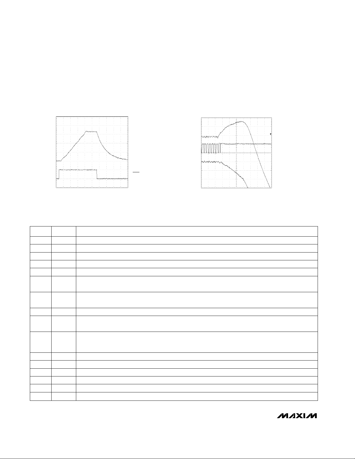
Figure 6 shows the output voltage response to a 0A to
3A load transient with and without the integrator. With
the integrator, the output voltage returns to within 0.1%
of its no-load value with only a small AC excursion.
Without the integrator, load regulation is degraded
(Figure 6b). Asymmetrical clamping at the integrator
output prevents worsening of load transients during
pulse-skipping mode.
Output Undervoltage Lockout
The output undervoltage-lockout circuit protects
against heavy overloads and short-circuits at the main
SMPS output. This scheme employs a timer rather than
a foldback current limit. The SMPS has an undervoltage-protection circuit, which is activated 6144 clock
cycles after the SMPS is enabled. If the SMPS output is
under 70% of the nominal value, it is latched off and
does not restart until SHDN is toggled. Applications
that use the recommended RC power-on-reset circuit
will also clear the fault condition when VCCfalls below
0.5V (typical). Note that undervoltage protection can
0
2
4
-50
50
I
OUT
(A)
V
OUT
(mV)
(100µs/div)
CC = 470pF
V
OUT
= 3.3V
INTEGRATOR
ACTIVE
Figure 6a. Load-Transient Response with Integrator Active
0
2
4
-50
50
I
OUT
(A)
V
OUT
(mV)
(100µs/div)
CC = REF
V
OUT
= 3.3V
INTEGRATOR
DEACTIVATED
Figure 6b. Load-Transient Response with Integrator
Deactivated
Page 14

MAX1637
Miniature, Low-Voltage,
Precision Step-Down Controller
14 ______________________________________________________________________________________
make prototype troubleshooting difficult since only
20ms or 30ms elapse before the SMPS is latched off.
The overvoltage crowbar protection is disabled in output undervoltage mode.
Output Overvoltage Protection
The overvoltage crowbar-protection circuit is intended
to blow a fuse in series with the battery if the main
SMPS output rises significantly higher than its standard
level (Table 4). In normal operation, the output is compared to the internal precision reference voltage. If the
output goes 7% above nominal, the synchronous-rectifier MOSFET turns on 100% (the high-side MOSFET is
simultaneously forced off) in order to draw massive
amounts of battery current to blow the fuse. This safety
feature does not protect the system against a failure of
the controller IC itself, but is intended primarily to guard
against a short across the high-side MOSFET. A crowbar event is latched and can only be reset by a rising
edge on SHDN (or by removal of the VCCsupply voltage). The overvoltage-detection decision is made relative to the regulation point.
Internal Digital Soft-Start Circuit
Soft-start allows a gradual increase of the internal current-limit level at start-up to reduce input surge currents. The SMPS contains an internal digital soft-start
circuit controlled by a counter, a digital-to-analog converter (DAC), and a current-limit comparator. In shutdown, the soft-start counter is reset to zero. When the
SMPS is enabled, its counter starts counting oscillator
pulses, and the DAC begins incrementing the comparison voltage applied to the current-limit comparator. The
DAC output increases from 0mV to 100mV in five equal
steps as the count increases to 512 clocks. As a result,
the main output capacitor charges up relatively slowly.
The exact time of the output rise depends on output
capacitance and load current, but it is typically 1ms
with a 300kHz oscillator.
Setting the Output Voltage
The output voltage is set via a resistor divider connected to FB (Figure 1). Calculate the output voltage with
the following formula:
V
OUT
= V
REF
(1 + R2 / R3)
where V
REF
= 1.1V nominal.
Recommended normal values for R3 range from 5kΩ to
100kΩ. To achieve a 1.1V nominal output, connect FB
directly to CSL. Remote output voltage sensing is possible by using the top of the external resistor divider as
the remote sense point.
__________________Design Procedure
The standard application circuit (Figure 1) contains a
ready-to-use solution for common application needs.
Use the following design procedure to optimize the
basic schematic for different voltage or current requirements. But before beginning a design, firmly establish
the following:
• Maximum input (battery) voltage, V
IN(MAX)
. This
value should include the worst-case conditions, such
as no-load operation when a battery charger or AC
adapter is connected but no battery is installed.
V
IN(MAX)
must not exceed 30V.
• Minimum input (battery) voltage, V
IN(MIN)
. This value
should be taken at full load under the lowest battery
conditions. If the minimum input-output difference is
less than 1.5V, the filter capacitance required to
maintain good AC load regulation increases (see
Low-Voltage Operation
section).
Table 4. Operating Modes
All circuit blocks offLowShutdown
REF = off, DL = lowHigh
Output
Undervoltage
Lockout
REF = off, DL = highHigh
Overvoltage
(Crowbar)
—
V
OUT
below 70% of
nominal after 20ms to
30ms timeout expires
V
OUT
greater than 7%
above regulation point
V
OUT
in regulation
CONDITIONSMODE
All circuit blocks activeHighRun
STATUS
SHDN
Lowest current consumption
Rising edge on SHDN exits
UVLO
Rising edge on SHDN exits
crowbar
Normal operation
NOTES
Page 15

MAX1637
Miniature, Low-Voltage,
Precision Step-Down Controller
______________________________________________________________________________________ 15
Inductor Value
The exact inductor value is not critical and can be
freely adjusted to allow trade-offs among size, cost,
and efficiency. Lower inductor values minimize size
and cost, but reduce efficiency due to higher peakcurrent levels. The smallest inductor value is obtained
by lowering the inductance until the circuit operates at
the border between continuous and discontinuous
mode. Further reducing the inductor value below this
crossover point results in discontinuous-conduction
operation, even at full load. This helps lower output filter
capacitance requirements, but efficiency suffers under
these conditions, due to high I2R losses. On the other
hand, higher inductor values produce greater efficiency, but also result in resistive losses due to extra wire
turns—a consequence that eventually overshadows the
benefits gained from lower peak current levels. High
inductor values can also affect load-transient response
(see the V
SAG
equation in the
Low-Voltage Operation
section). The equations in this section are for continuous-conduction operation.
Three key inductor parameters must be specified:
inductance value (L), peak current (I
PEAK
), and DC
resistance (RDC). The following equation includes a
constant, LIR, which is the ratio of inductor peak-topeak AC current to DC load current. A higher LIR value
allows lower inductance, but results in higher losses
and ripple. A good compromise is a 30% ripple-current
to load-current ratio (LIR = 0.3), which corresponds to a
peak inductor current 1.15 times higher than the DC
load current.
L = V
OUT(VIN(MAX)
- V
OUT
) / (V
IN(MIN)
x ƒ x I
OUT
x
LIR)
where ƒ = switching frequency (normally 200kHz or
300kHz), and I
OUT
= maximum DC load current.
The peak current can be calculated as follows:
I
PEAK
= I
LOAD
+ [V
OUT(VIN(MAX)
- V
OUT
) / (2 x ƒ x L
x V
IN(MAX)
)]
The inductor’s DC resistance should be low enough
that RDCx I
PEAK
< 100mV, as it is a key parameter for
efficiency performance. If a standard, off-the-shelf
inductor is not available, choose a core with an LI2rating greater than L x IPEAK2and wind it with the largest
diameter wire that fits the winding area. For 300kHz
applications, ferrite-core material is strongly preferred;
for 200kHz applications, Kool-Mu®(aluminum alloy) or
even powdered iron is acceptable. If light-load efficiency is unimportant (in desktop PC applications, for
example), then low-permeability iron-powder cores can
be acceptable, even at 300kHz. For high-current applications, shielded-core geometries (such as toroidal or
pot core) help keep noise, EMI, and switchingwaveform jitter low.
Current-Sense Resistor Value
The current-sense resistor value is calculated according to the worst-case, low-current limit threshold voltage (from the
Electrical Characteristics
) and the peak
inductor current:
R
SENSE
= 80mV / I
PEAK
Use I
PEAK
from the second equation in the
Inductor
Value
section. Use the calculated value of R
SENSE
to
size the MOSFET switches and specify inductor saturation-current ratings according to the worst-case highcurrent-limit threshold voltage:
I
PEAK
= 120mV / R
SENSE
Low-inductance resistors, such as surface-mount metal
film, are recommended.
Input Capacitor Value
Connect low-ESR bulk capacitors directly to the drain
on the high-side MOSFET. The bulk input filter capacitor is usually selected according to input ripple current
requirements and voltage rating, rather than capacitor
value. Electrolytic capacitors with low enough equivalent series resistance (ESR) to meet the ripple-current
requirement invariably have sufficient capacitance values. Aluminum electrolytic capacitors, such as Sanyo
OS-CON or Nichicon PL, are superior to tantalum
types, which risk power-up surge-current failure, especially when connecting to robust AC adapters or lowimpedance batteries. RMS input ripple current (I
RMS
) is
determined by the input voltage and load current, with
the worst case occurring at VIN= 2 x V
OUT
. Therefore,
when VINis 2 x V
OUT
:
I
RMS
= I
LOAD
/ 2
VCCand VGGshould be isolated from each other with a
20Ω resistor and bypassed to ground independently.
Place a 0.1µF capacitor between VCCand GND, as
close to the supply pin as possible. A 4.7µF capacitor
is recommended between VGGand PGND.
Output Filter Capacitor Value
The output filter capacitor values are generally determined by the ESR and voltage-rating requirements,
rather than by actual capacitance requirements for loop
stability. In other words, the low-ESR electrolytic capacitor that meets the ESR requirement usually has more
output capacitance than is required for AC stability.
Kool-Mu is a trademark of Magnetics, Inc.
Page 16

MAX1637
Miniature, Low-Voltage,
Precision Step-Down Controller
16 ______________________________________________________________________________________
Use only specialized low-ESR capacitors intended for
switching-regulator applications, such as AVX TPS,
Sprague 595D, Sanyo OS-CON, or Nichicon PL series.
To ensure stability, the capacitor must meet both minimum capacitance and maximum ESR values as given
in the following equations:
COUT > V
REF
(1 + V
OUT
/ V
IN(MIN)
) / V
OUT
x R
SENSE
x ƒ
R
ESR
< R
SENSE
x V
OUT
/ V
REF
where R
ESR
can be multiplied by 1.5, as discussed
below.
These equations are worst case, with 45 degrees of
phase margin to ensure jitter-free, fixed-frequency
operation, and provide a nicely damped output
response for zero to full-load step changes. Some costconscious designers may wish to bend these rules with
less-expensive capacitors, particularly if the load lacks
large step changes. This practice is tolerable if some
bench testing over temperature is done to verify
acceptable noise and transient response.
No well-defined boundary exists between stable and
unstable operation. As phase margin is reduced, the first
symptom is timing jitter, which shows up as blurred edges
in the switching waveforms where the scope does not quite
sync up. Technically speaking, this jitter (usually harmless)
is unstable operation since the duty factor varies slightly.
As capacitors with higher ESRs are used, the jitter
becomes more pronounced, and the load-transient output
voltage waveform starts looking ragged at the edges.
Eventually, the load-transient waveform has enough ringing
on it that the peak noise levels exceed the allowable output
voltage tolerance. Note that even with zero phase margin
and gross instability, the output voltage seldom declines
beyond I
PEAK
x R
ESR
(under constant loads).
Designers of RF communicators or other noise-sensitive analog equipment should be conservative and stay
within the guidelines. Designers of notebook computers
and similar commercial-temperature-range digital systems can multiply the R
ESR
value by a factor of 1.5
without affecting stability or transient response.
The output voltage ripple, which is usually dominated by
the filter capacitor’s ESR, can be approximated as
I
RIPPLE
x R
ESR
. There is also a capacitive term, so the
full equation for ripple in continuous-conduction mode is
V
RIPPLE(p-p)
= I
RIPPLE
x [R
ESR
+ 1 / (2πƒ x C
OUT
)]. In
idle mode, the inductor current becomes discontinuous,
with high peaks and widely spaced pulses, so the noise
can actually be higher at light load (compared to full
load). In idle mode, calculate the output ripple as follows:
V
RIPPLE(p-p)
= (0.02 x R
ESR
/ R
SENSE
) + [0.0003 x L x
(1 / V
OUT
+ 1 / (VIN- V
OUT
)) / R
SENSE
2
x CF]
Selecting Other Components
MOSFET Switches
The high-current N-channel MOSFETs must be logiclevel types with guaranteed on-resistance specifications
at VGS= 4.5V. Lower gate-threshold specifications are
better (i.e., 2V max rather than 3V max). Drain-source
breakdown voltage ratings must at least equal the maximum input voltage, preferably with a 20% margin. The
best MOSFETs have the lowest on-resistance per
nanocoulomb of gate charge. Multiplying R
DS(ON)
by
Qg provides a good figure of merit for comparing various MOSFETs. Newer MOSFET process technologies
with dense cell structures generally perform best. The
internal gate drivers tolerate >100nC total gate charge,
but 70nC is a more practical upper limit to maintain best
switching times.
In high-current applications, MOSFET package power
dissipation often becomes a dominant design factor.
I2R power losses are the greatest heat contributor for
both high-side and low-side MOSFETs. I2R losses are
distributed between Q1 and Q2 according to duty factor, as shown in the following equations. Generally,
switching losses affect only the upper MOSFET since
the Schottky rectifier usually clamps the switching node
before the synchronous rectifier turns on. Gate-charge
losses are dissipated by the driver and do not heat the
MOSFET. Calculate the temperature rise according to
package thermal-resistance specifications to ensure
that both MOSFETs are within their maximum junction
temperature at high ambient temperature. The worstcase dissipation for the high-side MOSFET occurs at
both extremes of input voltage, and the worst-case dissipation for the low-side MOSFET occurs at maximum
input voltage.
Duty = (V
OUT
+ VQ2) / (VIN- VQ1)
P
D (UPPER FET)
= I
LOAD
2
x R
DS(ON)
x duty + VINx
I
LOAD
x ƒ x [(VINx C
RSS
) / I
GATE
+ 20ns]
P
D (LOWER FET)
= I
LOAD
2
x R
DS(ON)
x (1 - duty)
where VQ= the on-state voltage drop (I
LOAD
x
R
DS(ON)
), C
RSS
= the MOSFET reverse transfer capaci-
tance, I
GATE
= the DH driver peak output current capability (1A typ), and the DH driver inherent rise/fall time is
20ns. The MAX1637’s output undervoltage shutdown
function protects the synchronous rectifier under output
short-circuit conditions. To reduce EMI, add a 0.1µF
ceramic capacitor from the high-side switch drain to
the low-side switch source.
Page 17

Rectifier Clamp Diode
The rectifier is a clamp across the low-side MOSFET
that catches the negative inductor swing during the
60ns dead time between turning one MOSFET off and
turning each low-side MOSFET on. The latest generations of MOSFETs incorporate a high-speed silicon
body diode, which serves as an adequate clamp diode
if efficiency is not of primary importance. A Schottky
diode can be placed in parallel with the body diode to
reduce the forward voltage drop, typically improving
efficiency 1% to 2%. Use a diode with a DC current rating equal to one-third of the load current; for example,
use an MBR0530 (500mA-rated) type for loads up to
1.5A, a 1N5819 type for loads up to 3A, or a 1N5822
type for loads up to 10A. The rectifier’s rated reversebreakdown voltage must be at least equal to the maximum input voltage, preferably with a 20% margin.
Boost-Supply Diode D2
A signal diode such as a 1N4148 works well in most
applications. Do not use large power diodes, such as
1N5817 or 1N4001.
Low-Voltage Operation
Low input voltages and low input-output differential voltages each require extra care in their design. Low
VIN-V
OUT
differentials can cause the output voltage to
sag when the load current changes abruptly. The sag’s
amplitude is a function of inductor value and maximum
duty factor (D
MAX
, an
Electrical Characteristics
parameter, 93% guaranteed over temperature at f = 200kHz) as
follows:
V
SAG
= [(I
STEP
)2x L] / [2CFx (V
IN(MIN)
x D
MAX
-
V
OUT
)]
Table 5 is a low-voltage troubleshooting guide. The
cure for low-voltage sag is to increase the output
capacitor’s value. For example, at VIN= 5.5V, V
OUT
=
5V, L = 10µH, ƒ = 200kHz, and I
STEP
= 3A, a total
capacitance of 660µF keeps the sag below 200mV.
Note that only the capacitance requirement increases;
the ESR requirements do not change. Therefore, the
added capacitance can be supplied by a low-cost bulk
capacitor in parallel with the normal low-ESR capacitor.
__________Applications Information
Heavy-Load Efficiency Considerations
The major efficiency-loss mechanisms under loads are
as follows, in the usual order of importance:
• P(I2R) = I2R losses
• P(tran) = transition losses
• P(gate) = gate-charge losses
• P(diode) = diode-conduction losses
• P(cap) = capacitor ESR losses
• P(IC) = losses due to the IC’s operating supply current
Inductor core losses are fairly low at heavy loads
because the inductor’s AC current component is small.
Therefore, these losses are not considered in this
analysis. Ferrite cores are preferred, especially at
300kHz, but powdered cores, such as Kool-Mu, can
also work well.
Efficiency = P
OUT
/ PINx 100%
= P
OUT
/ (P
OUT
+ P
TOTAL
) x 100%
P
TOTAL
= P(I2R) + P(tran) + P(gate) + P(diode) +
P(cap) + P(IC)
P = (I2R) = I
LOAD
2
x (RDC+ R
DS(ON)+RSENSE
)
where RDCis the DC resistance of the coil, R
DS(ON)
is
the MOSFET on-resistance, and R
SENSE
is the current-
sense resistor value. The R
DS(ON)
term assumes identical MOSFETs for the high-side and low-side switches
because they time-share the inductor current. If the
MOSFETs are not identical, their losses can be estimated by averaging the losses according to duty factor.
PD(tran) = transition loss = VINx I
LOAD
x ƒ x
[(VINC
RSS
/ I
GATE
) + 20ns]
where C
RSS
is the reverse transfer capacitance of the
high-side MOSFET (a data sheet parameter), I
GATE
is
the DH gate-driver peak output current (1.5A typ), and
the rise/fall time of the DH driver is typically 20ns.
MAX1637
Miniature, Low-Voltage,
Precision Step-Down Controller
______________________________________________________________________________________ 17
Table 5. Low-Voltage Troubleshooting Guide
Low VIN-V
OUT
differential,
under 1V
Low VIN-V
OUT
differential,
under 1.5V
Dropout voltage is
too high
Sag or droop in V
OUT
under step-load change
SYMPTOM
Maximum duty-cycle limits
exceeded
Limited inductor-current
slew rate per cycle
ROOT CAUSECONDITION
Reduce operation to 200kHz.
Reduce MOSFET on-resistance
and coil DC resistance.
Increase bulk output capacitance
per formula (see
Low-Voltage
Operation
section). Reduce
inductor value.
SOLUTION
Page 18

MAX1637
P(gate) = Qgx ƒ x V
GG
where Qgis the sum of the gate-charge values for lowside and high-side switches. For matched MOSFETs,
Qgis twice the data-sheet value of an individual
MOSFET. Efficiency can usually be optimized by connecting VGGto the most efficient 5V source, such as
the system +5V supply.
P(diode) = diode conduction losses = I
LOAD
x V
FWD
x tDx ƒ
where tDis the diode conduction time (120ns typ), and
V
FWD
is the diode forward voltage. This power is dissipated in the MOSFET body diode if no external
Schottky diode is used.
P(cap) = input capacitor ESR loss = I
RMS
2
x R
ESR
where I
RMS
is the input ripple current as calculated in
the
Input Capacitor Value
section.
Light-Load Efficiency Considerations
Under light loads, the PWM operates in discontinuous
mode. The inductor current discharges to zero at some
point during the charging cycle. This makes the inductor current’s AC component high compared to the load
current, which increases core losses and I2R losses in
the input-output filter capacitors. For best light-load efficiency, use MOSFETs with moderate gate-charge levels and use ferrite MPP or other low-loss core material.
Avoid powdered-iron cores; even Kool-Mu (aluminum
alloy) is not as desirable as ferrite.
Low-Noise Operation
Noise-sensitive applications such as hi-fidelity multimedia-equipped systems, cellular phones, RF communicating computers, and electromagnetic pen-entry
systems should operate the controller in PWM mode
(SKIP = high). This mode forces a constant switching
frequency, reducing interference due to switching
noise by concentrating the radiated EM fields at a
known frequency outside the system audio or IF bands.
Choose an oscillator frequency for which switchingfrequency harmonics do not overlap a sensitive frequency band. If necessary, synchronize the oscillator
to a tight-tolerance external clock generator.
Powering From a Single
Low-Voltage Supply
The circuit of Figure 7 is powered from a single 3.3V to
5.5V source and delivers 4A at 2.5V. At input voltages
of 3.15V, this circuit typically achieves efficiencies of
90% at 3.5A load currents. When using a single supply
to power both V
BATT
and V
BIAS
, be sure that it does not
exceed the 5.5V rating (6V absolute maximum) for V
GG
and VCC. Also, heavy current surges from the input
may cause transient dips on VCC. To prevent this, the
decoupling capacitor on VCCmay need to be
increased to 2µF or greater. This circuit uses lowthreshold (specified at VGS= 2.7V) IRF7401 MOSFETs
which allow a typical startup of 3.15V at above 4A. Low
input voltages demand the use of larger input capacitors. Sanyo OS-CONs are recommended for their high
capacity and low ESR.
PC Board Layout Considerations
Good PC board layout is required to achieve specified
noise, efficiency, and stable performance. The PC
board layout artist must be given explicit instructions,
preferably a pencil sketch showing the placement of
power-switching components and high-current routing.
See the PC board layout in the MAX1637 evaluation kit
manual for examples. A ground plane is essential for
optimum performance. In most applications, the circuit
will be located on a multi-layer board, and full use of
the four or more copper layers is recommended. Use
the top layer for high-current connections, the bottom
layer for quiet connections (REF, CC, GND), and the
inner layers for an uninterrupted ground plane. Use the
following step-by-step guide:
1) Place the high-power components (C1, C2, Q1, Q2,
D1, L1, and R1) first, with their grounds adjacent.
•
Minimize current-sense resistor trace lengths
and
ensure accurate current sensing with Kelvin connections (Figure 8).
•
Minimize ground trace lengths
in the high-current
paths.
•
Minimize other trace lengths
in the high-current
paths.
— Use >5mm-wide traces.
— CIN to high-side MOSFET drain: 10mm
max length
— Rectifier diode cathode to low side
— MOSFET: 5mm max length
— LX node (MOSFETs, rectifier cathode, induc-
tor): 15mm max length
Ideally, surface-mount power components are butted
up to one another with their ground terminals almost
touching. These high-current grounds are then connected to each other with a wide, filled zone of
top-layer copper so they do not go through vias. The
resulting top-layer subground plane is connected to the
normal inner-layer ground plane at the output ground
terminals, which ensures that the IC’s analog ground is
Miniature, Low-Voltage,
Precision Step-Down Controller
18 ______________________________________________________________________________________
Page 19

sensing at the supply’s output terminals without interference from IR drops and ground noise. Other high-current paths should also be minimized, but focusing
primarily on short ground and current-sense connections eliminates about 90% of all PC board layout problems (see the PC board layouts in the MAX1637
evaluation kit manual for examples).
2) Place the IC and signal components. Keep the main
switching nodes (LX nodes) away from sensitive
analog components (current-sense traces and REF
capacitor). Place the IC and analog components on
the opposite side of the board from the powerswitching node. Important: The IC must be no further than 10mm from the current-sense resistors.
Keep the gate-drive traces (DH, DL, and BST) shorter than 20mm and route them away from CSH, CSL,
and REF. Place ceramic bypass capacitors close to
the IC. The bulk capacitors can be placed further
away.
3) Use a single-point star ground where the input
ground trace, power ground (subground plane), and
normal ground plane meet at the supply's output
ground terminal. Connect both IC ground pins and
all IC bypass capacitors to the normal ground plane.
MAX1637
Miniature, Low-Voltage,
Precision Step-Down Controller
______________________________________________________________________________________ 19
MAX1637
SENSE RESISTOR
HIGH-CURRENT PATH
Figure 8. Kelvin Connections for the Current-Sense Resistors
MAX1637
0.1µF
1µF
IRF7401
CMPSH-3
IRF7401
1µF
470pF
MBRS130
470µF
LOW ESR
TANTALUM
4.7µF
TANTALUM
220µF
OS-CON
V
BIAS
10µH
CDHR125-100
20mΩ
1%
130k
1%
100k
1%
OUTPUT = 2.5V AT 4A
V
CC
20Ω
GND CC
DL
LX
DH
BST
V
GG
CSH
CSL
FB
SHDN
ON/OFF
SKIP
SYNC
REF
PGND
3.15V TO 5.5V
Figure 7. 3.15V to 5.5V Single-Supply Application Circuit
Page 20

MAX1637
Miniature, Low-Voltage,
Precision Step-Down Controller
Maxim cannot assume responsibility for use of any circuitry other than circuitry entirely embodied in a Maxim product. No circuit patent licenses are
implied. Maxim reserves the right to change the circuitry and specifications without notice at any time.
20
____________________Maxim Integrated Products, 120 San Gabriel Drive, Sunnyvale, CA 94086 408-737-7600
© 1998 Maxim Integrated Products Printed USA is a registered trademark of Maxim Integrated Products.
___________________Chip Information
________________________________________________________Package Information
TRANSISTOR COUNT: 2164
QSOP.EPS
 Loading...