

Page 1
_______________General Description
The MAX1624/MAX1625 are ultra-high-performance,
step-down DC-DC controllers for CPU power in high-end
computer systems. Designed for demanding applications
in which output voltage precision and good transient
response are critical for proper operation, they deliver
over 35A from 1.1V to 3.5V with ±1% total accuracy from
a +5V ±10% supply. Excellent dynamic response corrects output transients caused by the latest dynamically
clocked CPUs. These controllers achieve over 90% efficiency by using synchronous rectification. Flying-capacitor bootstrap circuitry drives inexpensive, external
N-channel MOSFETs.
The switching frequency is resistor programmable from
100kHz to 1MHz. High switching frequencies allow the
use of a small surface-mount inductor and decrease output filter capacitor requirements, reducing board area
and system cost.
The MAX1624 is available in a 24-pin SSOP and offers
additional features such as a digitally programmable output in 100mV increments; adjustable transient response;
selectable 0.5%, 1%, or 2% AC load regulation; and gate
drive for a current-boost MOSFET. The MAX1625 is resistor adjustable and comes in a 16-pin narrow SO package. Other features in both controllers include internal
digital soft-start, a power-good output, and a 3.5V ±1%
reference output. For a similar controller compatible with
the latest Intel V
RM/VID
specification, see the MAX1638*
data sheet.
________________________Applications
Pentium Pro™, Pentium II™, PowerPC™, Alpha™,
and K6™ Systems
Desktop Computers
LAN Servers
Industrial Computers
GTL Bus Termination
____________________________Features
♦ Better than ±1% Output Accuracy Over
Line and Load
♦ 90% Efficiency
♦ Excellent Transient Response
♦ Resistor-Programmable Fixed Switching
Frequency from 100kHz to 1MHz
♦ Over 35A Output Current
♦ Digitally Programmable Output from 1.1V to 3.5V
in 100mV Increments (MAX1624)
♦ Resistor-Adjustable Output down to 1.1V
(MAX1625)
♦ Remote Sensing
♦ Adjustable AC Loop Gain (MAX1624)
♦ GlitchCatcher™ Circuit for Fast Load-Transient
Response (MAX1624)
♦ Power-Good (PWROK) Output
♦ Current-Mode Feedback
♦ Digital Soft-Start
♦ Strong 2A Gate Drivers
♦ Current-Limited Output
MAX1624/MAX1625
High-Speed Step-Down Controllers with
Synchronous Rectification for CPU Power
________________________________________________________________
Maxim Integrated Products
1
19-1227; Rev 1; 6/97
PART
MAX1624EAG
MAX1625ESE
-40°C to +85°C
-40°C to +85°C
TEMP. RANGE PIN-PACKAGE
24 SSOP
16 Narrow SO
______________Ordering Information
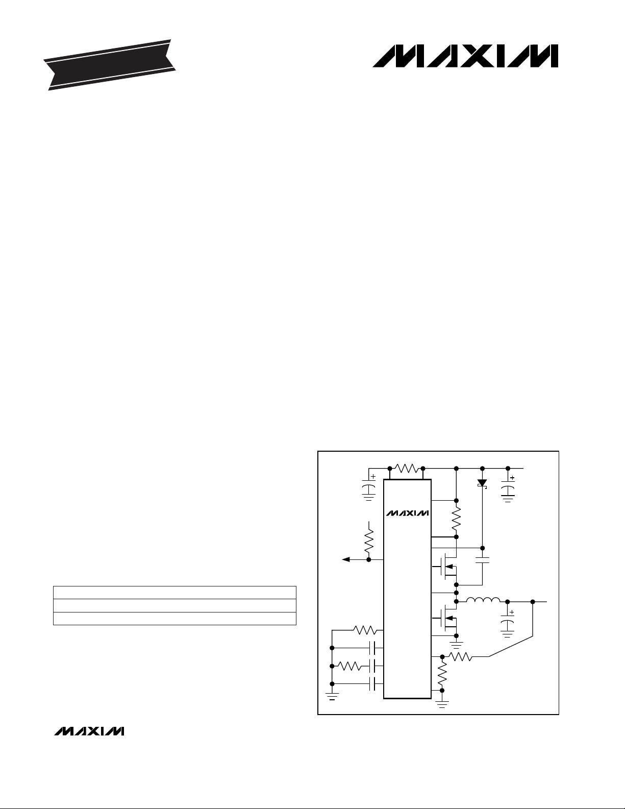
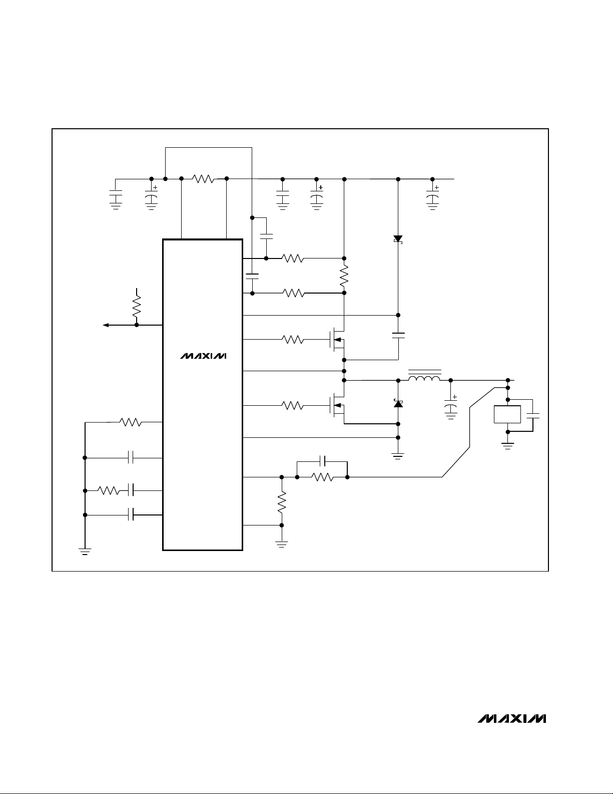
__________Typical Operating Circuit
Pin Configurations appear at end of data sheet.
*
Future product.
Pentium Pro and Pentium II are trademarks of Intel Corp.
PowerPC is a trademark of IBM Corp.
Alpha is a trademark of Digital Equipment Corp.
K6 is a trademark of Advanced Micro Devices.
GlitchCatcher is a trademark of Maxim Integrated Products.
EVALUATION KIT
AVAILABLE
V
CC
FREQ
CC2
CC1
REF
AGND
(SIMPLIFIED)
FB
DL
DH
PWROK
BST
CSL
CSH
LX
TO V
DD
TO AGND
PGND
OUTPUT
1.1V TO 4.5V
INPUT
+5V
V
DD
N
N
MAX1625
For free samples & the latest literature: http://www.maxim-ic.com, or phone 1-800-998-8800.
For small orders, phone 408-737-7600 ext. 3468.
Page 2
kHz
MAX1624/MAX1625
High-Speed Step-Down Controllers with
Synchronous Rectification for CPU Power
2 _______________________________________________________________________________________
ABSOLUTE MAXIMUM RATINGS
ELECTRICAL CHARACTERISTICS
(VDD= V
CC
= D4 = +5V, PGND = AGND = D0–D3 = 0V, R
FREQ
= 33.3kΩ, TA= 0°C to +85°C, unless otherwise noted.)
Stresses beyond those listed under “Absolute Maximum Ratings” may cause permanent damage to the device. These are stress ratings only, and functional
operation of the device at these or any other conditions beyond those indicated in the operational sections of the specifications is not implied. Exposure to
absolute maximum rating conditions for extended periods may affect device reliability.
VDD, VCC, PWROK to AGND......................................-0.3V to 6V
PGND to AGND ..................................................................±0.3V
CSH, CSL to AGND....................................-0.3V to (VCC+ 0.3V)
NDRV, PDRV, DL to PGND.........................-0.3V to (VDD+ 0.3V)
REF, CC1, CC2, LG, D0–D4, FREQ,
FB to AGND................................................-0.3V to (V
CC
+ 0.3V)
BST to PGND............................................................-0.3V to 12V
BST to LX....................................................................-0.3V to 6V
DH to LX.............................................(LX - 0.3V) to (BST + 0.3V)
Continuous Power Dissipation (TA= ±70°C)
24 Pin SSOP (derate 8.00mW/°C above +70°C) ..........640mW
16 Pin Narrow SO (derate 8.70mW/°C above 70°C).....696mW
Operating Temperature Range
MAX162_E_ _.......................................................-40°C to +85°C
Storage Temperature Range.............................-65°C to +125°C
Lead Temperature (soldering, 10sec).............................+300°C
R
FREQ
= 33.3kΩ
R
FREQ
= 20kΩ
PWROK = 5.5V
VCC= VDD= 5.5V,
FB overdrive = 200mV
I
SINK
= 2mA, VCC= 4.5V
Falling FB, 1% hysteresis with respect to V
REF
VCCrising edge, 1% hysteresis
Rising FB, 1% hysteresis with respect to V
REF
VCC= V
DD
MAX1624, over line
and load (Note 1)
V
REF
= 0V
Rising edge, 1% hysteresis
0µA < I
LOAD
< 100µA
VCC= VDD= 5.5V, FB overdrive = 200mV,
operating or standby mode
MAX1625, over line
and load (Note 2)
No load
CONDITIONS
540 600 660
850 1000 1150
Switching Frequency
µA1PWROK Output Current High
V0.4PWROK Output Voltage Low
6.5 8 9.5
%
-7.5 -6 -4.5
PWROK Trip Level
1
2
1
%
0.5
AC Load Regulation
(Note 3)
±1.5
%
±1
FB Set Voltage
±1.5
2.5
VCCSupply Current
V4.0 4.2
V4.5 5.5Input Voltage Range
Input Undervoltage Lockout
%
±1
FB Accuracy
mA0.5 4.0Reference Short-Circuit Current
V2.7 3.0Reference Undervoltage Lockout
mV10Reference Load Regulation
mA
0.3
mA0.1VDDSupply Current
V3.465 3.5 3.535Reference Voltage
UNITSMIN TYP MAXPARAMETER
Operating mode
Standby mode
TA= +25°C to +85°C
TA= 0°C to +85°C
TA= +25°C to +85°C
TA= 0°C to +85°C
CSH - CSL =
0mV to 80mV
R
FREQ
= 200kΩ
kHz
85 100 115
LG = REF
LG = GND
LG = V
CC
MAX1624
MAX1625
LG = REF
CSH - CSL =
0mV to 80mV
LG = GND
LG = V
CC
0.1
MAX1624
MAX1625
0.2
0.1
%
0.05
DC Load Regulation
(Note 3)
Page 3
ELECTRICAL CHARACTERISTICS (continued)
(VDD= V
CC
= D4 = +5V, PGND = AGND = D0–D3 = 0V, R
FREQ
= 33.3kΩ, TA= 0°C to +85°C, unless otherwise noted.)
MAX1624/MAX1625
_______________________________________________________________________________________
3
DH = DL = 2.5V
VDD= 4.5V
BST - LX = 4.5V
LG = GND (low)
100mV overdrive
R
FREQ
= 20kΩ
With respect to V
REF
,
FB going low
Minimum
MAX1625, CSH = CSL = 1.1V
D0–D4 = 0V, 5V
D0–D4; VCC= 4.5V
LG = REF (mid)
MAX1624, CSH = CSL = 1.3V,
D0–D3 = 5V, D4 = 0V
D0–D4; VCC= 5.5V
CONDITIONS
-2.75 -2 -1.25
LG = V
CC
(high)
ns0 30
FB = 1.1V
DH, DL Dead Time
A2DH, DL Source/Sink Current
Ω
0.7 2
Maximum
DH On-Resistance 0.7 2
%
-3 -1
µA100CC2 Source/Sink Current
4 V
CC
V
2.4 3.0
mmho1
kΩ10CC1 Output Resistance
µA±0.1
50
3.3 3.7
0.2
%85 90Maximum Duty Cycle
LG Input Voltage
µA
50
CSH, CSL Input Current
µA4LG Input Current
µA±1D0–D4 Input Current
V2.0Logic Input Voltage High
VCC- 0.2
V
0.8Logic Input Voltage Low
UNITSMIN TYP MAXPARAMETER
FB Input Current
CC2 Clamp Voltage
CC2 Transconductance
PDRV Trip Level
PDRV, NDRV Response Time FB overdrive = 5% ns75
PDRV, NDRV On-Resistance VDD= 4.5V Ω2 5
PDRV, NDRV Source/Sink Current PDRV = NDRV = 2.5V A0.5
PDRV, NDRV Minimum On-Time ns100
Current-Limit Trip Voltage mV85 100 115
Soft-Start Time To full current limit 1 / f
OSC
1536
BST Leakage Current BST = 12V, LX = 7V, REF = GND µA50
V
High-Speed Step-Down Controllers with
Synchronous Rectification for CPU Power
ΩDL On-Resistance
NDRV Trip Level
With respect to V
REF
,
FB going high
1.25 2 2.75
%
1 3
TA= +25°C
TA= 0°C to +85°C
TA= +25°C
TA= 0°C to +85°C
Page 4
mA
MAX1624/MAX1625
High-Speed Step-Down Controllers with
Synchronous Rectification for CPU Power
4 _______________________________________________________________________________________
R
FREQ
= 33.3kΩ
R
FREQ
= 20kΩ
VCC= VDD= 5.5V,
FB overdrive = 200mV
Falling FB, 1% hysteresis with respect to V
REF
VCCrising edge, 1% hysteresis
Rising FB, 1% hysteresis with respect to V
REF
VCC= V
DD
R
FREQ
= 200kΩ
Operating mode
VCC= VDD= 5.5V, FB overdrive = 200mV,
operating or standby mode
MAX1624, over line and load
No load
CONDITIONS
510 600 690
Standby mode
800 1000 1200
Switching Frequency
6 8 10
kHz
80 100 120
%
-8 -6 -4
PWROK Trip Level
±2.5
3
VCCSupply Current
V3.9 4.3
V4.5 5.5Input Voltage Range
Input Undervoltage Lockout
%±2.5FB Accuracy
mA
0.4
mA0.2VDDSupply Current
V3.447 3.5 3.553Reference Voltage
UNITSMIN TYP MAXPARAMETER
MAX1625FB Set Voltage
BST - LX = 4.5V
R
FREQ
= 20kΩ
VDD= 4.5V
Ω0.7 2
%84 90
Ω0.7 2
Maximum Duty Cycle
DL On-Resistance
DH On-Resistance
Current-Limit Trip Voltage mV70 100 130
ELECTRICAL CHARACTERISTICS
(VDD= VCC= D4 = +5V, PGND = AGND = D0–D3= 0V, R
FREQ
= 33.3kΩ, TA= -40°C to +85°C, unless otherwise noted.) (Note 4)
Note 1: FB accuracy is 100% tested at FB = 3.5V (code 10000) with V
CC
= VDD= 4.5V to 5.5V and CSH - CSL = 0mV to 80mV. The
other DAC codes are tested at the major transition points with V
CC
= VDD= 5V and CSH - CSL = 0. FB accuracy at other
DAC codes over line and load is guaranteed by design.
Note 2: FB set voltage is 100% tested with VCC= VDD= 4.5V to 5.5V and CSH - CSL = 0mV to 80mV.
Note 3: AC load regulation sets the AC loop gain, to make tradeoffs between output filter capacitor size and transient response,
and has only a slight effect on DC accuracy or DC load-regulation error.
Note 4: Specifications from 0°C to -40°C are not production tested.
%
Page 5
MAX1624/MAX1625
High-Speed Step-Down Controllers with
Synchronous Rectification for CPU Power
_______________________________________________________________________________________ 5
__________________________________________Typical Operating Characteristics
(TA = +25°C, using the MAX1624 evaluation kit, unless otherwise noted.)
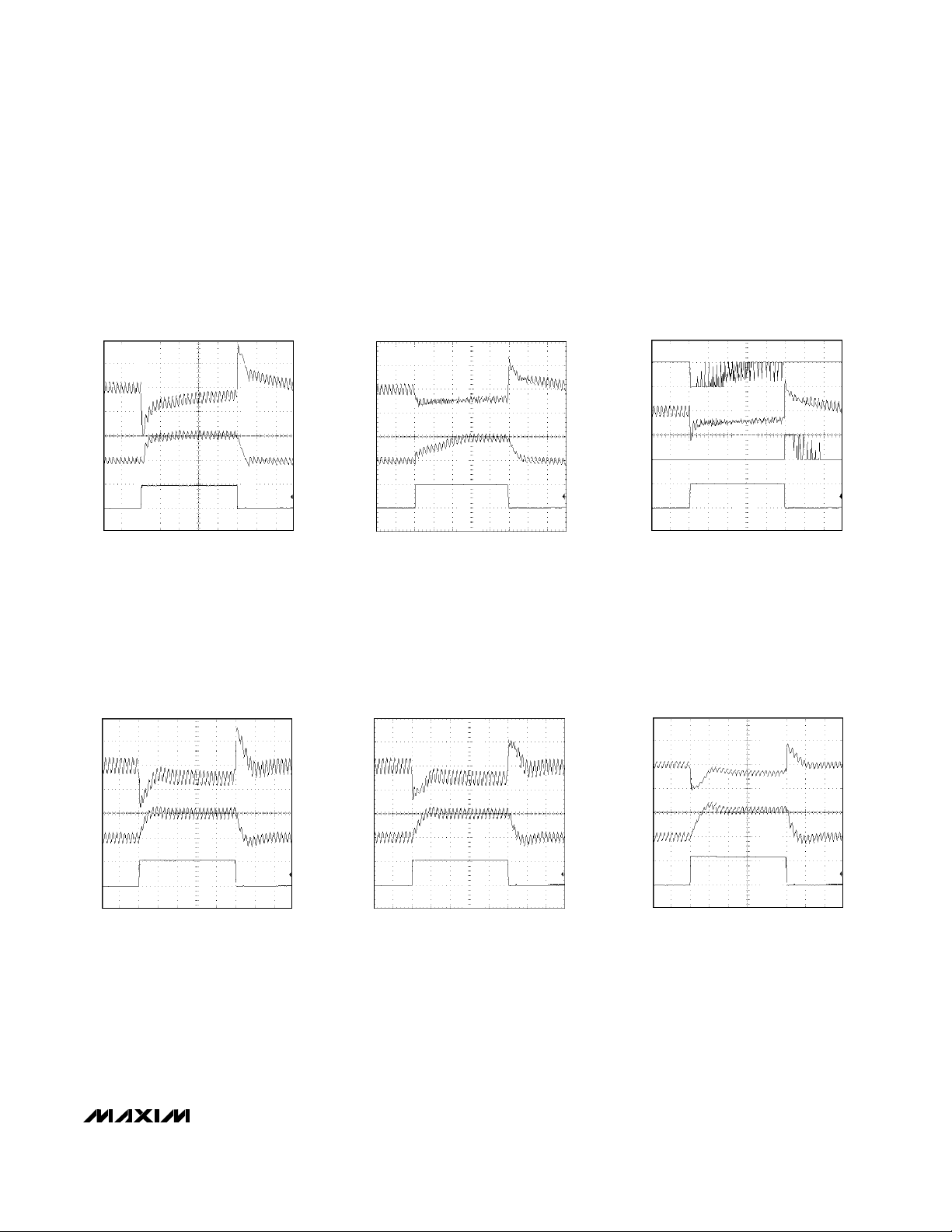
10µs/div
MAX1624
LOAD-TRANSIENT RESPONSE DETAIL
(WITH GLITCHCATCHER)
(1.1V)
C
D
MAX1624/25 TOC01
A: PDRV, 5V/div
B: V
OUT
, 50mV/div, AC COUPLED
C: NDRV, 5V/div
D: LOAD CURRENT, 0A TO 10A, t
RISE
= t
FALL
= 100ns
B
A
LG = REF
10µs/div
MAX1624
LOAD-TRANSIENT RESPONSE
(WITH GLITCHCATCHER)
(1.1V )
C
MAX1624/25 TOC02
A: V
OUT
, 50mV/div, AC COUPLED
B: INDUCTOR CURRENT, 10A/div
C: LOAD CURRENT, 0A TO 10A, t
RISE
= t
FALL
= 100ns
B
A
LG = REF
10µs/div
MAX1624
LOAD-TRANSIENT RESPONSE
(WITHOUT GLITCHCATCHER)
(1.1V)
C
MAX1624/25 TOC03
A: V
OUT
, 50mV/div, AC COUPLED
B: INDUCTOR CURRENT, 10A/div
C: LOAD CURRENT, 0A TO 10A, t
RISE
= t
FALL
= 100ns
B
A
LG = REF
10µs/div
MAX1624
LOAD-TRANSIENT RESPONSE
(WITHOUT GLITCHCATCHER)
(3.5V)
C
MAX1624/25 TOC15
A: V
OUT
, 100mV/div, AC COUPLED
B: INDUCTOR CURRENT, 10A/div
C: LOAD CURRENT, 0A TO 11A, t
RISE
= t
FALL
= 100ns
B
A
LG = REF
10µs/div
MAX1624
LOAD-TRANSIENT RESPONSE
(WITH GLITCHCATCHER)
(2.5V)
C
MAX1624/25 TOC17
A: V
OUT
, 50mV/div, AC COUPLED
B: INDUCTOR CURRENT, 10A/div
C: LOAD CURRENT, 0A TO 10A, t
RISE
= t
FALL
= 100ns
B
A
LG = REF
10µs/div
MAX1624
LOAD-TRANSIENT RESPONSE
(WITHOUT GLITCHCATCHER)
(2.5V)
C
MAX1624/25 TOC18
A: V
OUT
, 50mV/div, AC COUPLED
B: INDUCTOR CURRENT, 10A/div
C: LOAD CURRENT, 0A TO 10A, t
RISE
= t
FALL
= 100ns
B
A
LG = REF
Page 6
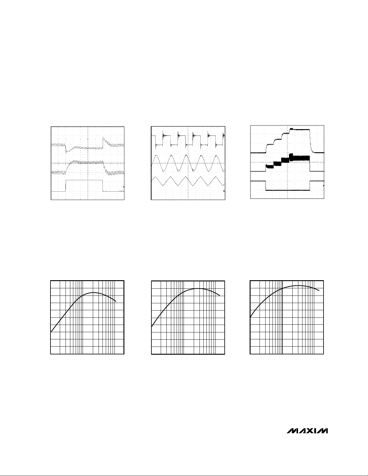
10µs/div
MAX1624
LOAD-TRANSIENT RESPONSE
(WITH GLITCHCATCHER)
(3.5V)
C
MAX1624/25 TOC16
A: V
OUT
, 100mV/div, AC COUPLED
B: INDUCTOR CURRENT, 10A/div
C: LOAD CURRENT, 0A TO 11A, t
RISE
= t
FALL
= 100ns
B
A
LG = REF
1µs/div
MAX1624
SWITCHING WAVEFORMS
C
0
MAX1624/25 TOC10
VIN = 5V, V
OUT
= 2.5V, LOAD = 5A
A: LX, 5V/div
B: V
OUT
, 20mV/div, AC COUPLED
C: INDUCTOR CURRENT, 5A/div
B
A
1ms/div
MAX1624
STARTUP AND STANDBY RESPONSE
C
MAX1624/25 TOC11
VIN = 5V, V
OUT
= 2.5V, LOAD = 13.8A
A: V
OUT
, 1V/div
B: INDUCTOR CURRENT, 10A/div
C: STANDBY, D0–D4
B
A
MAX1624/MAX1625
High-Speed Step-Down Controllers with
Synchronous Rectification for CPU Power
6 _______________________________________________________________________________________
____________________________Typical Operating Characteristics (continued)
(TA = +25°C, using the MAX1624 evaluation kit, unless otherwise noted.)
100
0
0.1 1 10
MAX1624
EFFICIENCY vs. OUTPUT CURRENT
(V
OUT
= 1.1V)
20
10
MAX1624/25 TOC04
OUTPUT CURRENT (A)
EFFICIENCY (%)
40
30
60
70
50
80
90
100
0
0.1 1 10
MAX1624
EFFICIENCY vs. OUTPUT CURRENT
(V
OUT
= 2.5V)
20
10
MAX1624/25 TOC05
OUTPUT CURRENT (A)
EFFICIENCY (%)
40
30
60
70
50
80
90
100
0
0.1 1 10
MAX1624
EFFICIENCY vs. OUTPUT CURRENT
(V
OUT
= 3.5V)
20
10
MAX1624/25 TOC06
OUTPUT CURRENT (A)
EFFICIENCY (%)
40
30
60
70
50
80
90
Page 7
MAX1624/MAX1625
High-Speed Step-Down Controllers with
Synchronous Rectification for CPU Power
_______________________________________________________________________________________ 7
____________________________Typical Operating Characteristics (continued)
(TA = +25°C, using the MAX1624 evaluation kit, unless otherwise noted.)
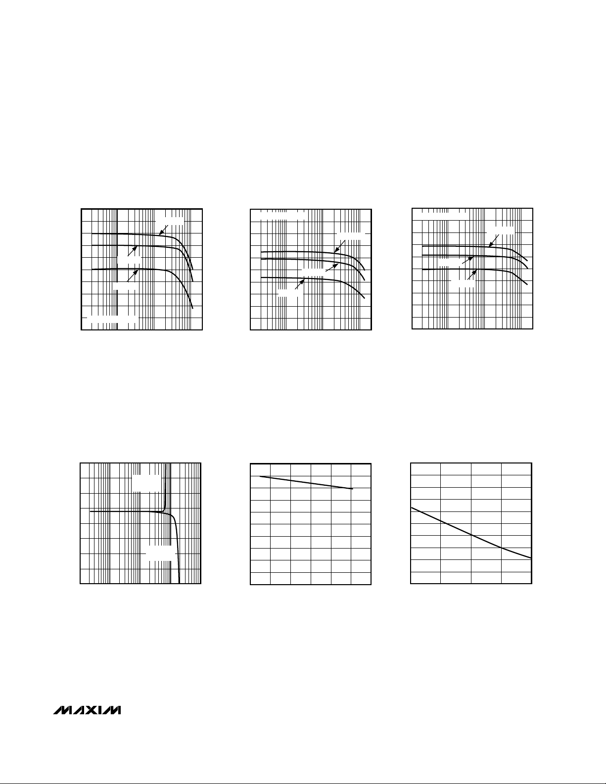
1.1020
1.1000
0.1 10.01 10
MAX1624
OUTPUT VOLTAGE vs. OUTPUT CURRENT
(V
OUT
= 1.1V)
1.1002
1.1006
1.1004
MAX1624/25 TOC07
OUTPUT CURRENT (A)
OUTPUT VOLTAGE (V)
1.1008
1.1010
1.1014
1.1012
1.1016
1.1018
LG = V
CC
LG = REF
LG = AGND
R9 AND R10 = 4.7Ω
2.500
2.490
0.1 10.01 10
MAX1624
OUTPUT VOLTAGE vs. OUTPUT CURRENT
(V
OUT
= 2.5V)
2.491
2.492
MAX1624/25 TOC08
OUTPUT CURRENT (A)
OUTPUT VOLTAGE (V)
2.493
2.494
2.496
2.495
2.497
2.498
2.499
LG = V
CC
LG = REF
LG = AGND
R9 AND R10 = 4.7Ω
3.500
3.480
0.1 10.01 10
MAX1624
OUTPUT VOLTAGE vs. OUTPUT CURRENT
(V
OUT
= 3.5V)
3.482
3.486
3.484
MAX1624/25 TOC09
OUTPUT CURRENT (A)
OUTPUT VOLTAGE (V)
3.488
3.494
3.490
3.492
3.496
3.498
LG = V
CC
LG = REF
LG = AGND
R9 AND R10 = 4.7Ω
5.094
1.094
0.001 0.1 10.01 10
REFERENCE VOLTAGE
vs. OUTPUT CURRENT
1.594
2.094
MAX1624/25 TOC12
OUTPUT CURRENT (mA)
REFERENCE VOLTAGE (V)
2.594
3.594
3.094
4.094
4.594
SOURCING
CURRENT
SINKING
CURRENT
50
55
0
MAXIMUM DUTY CYCLE
vs. SWITCHING FREQUENCY
65
60
70
MAX1624/25 tTOC13
SWITCHING FREQUENCY (kHz)
MAXIMUM DUTY CYCLE (%)
85
95
90
75
80
200 800 1000 1200
100
600400
10
-10
1.7 2.3 2.91.1 3.5
MAX1624
OUTPUT ERROR vs.
DAC OUTPUT VOLTAGE SETTING
-8
-4
-6
MAX1624/25 TOC19
DAC OUTPUT VOLTAGE SETTING (V)
OUTPUT ERROR (mV)
-2
4
0
2
6
8
Page 8
MAX1624/MAX1625
High-Speed Step-Down Controllers with
Synchronous Rectification for CPU Power
8 _______________________________________________________________________________________
MAX1625MAX1624
PIN
High-Side Main MOSFET Switch Gate-Drive Output. DH is a floating driver output that
swings from LX to BST, riding on the LX switching-node voltage. See the section
BST
High-Side Gate-Driver Supply and MOSFET Drivers
.
DH1624
Switching Node. Connect LX to the high-side MOSFET source and inductor.LX1523
Power GroundPGND1422
DL
Low-Side Synchronous Rectifier Gate-Drive Output. DL swings between PGND and VDD.
See the section
BST High-Side Gate-Driver Supply and MOSFET Drivers
.
1321
V
DD
5V Power Input for MOSFET Drivers. Bypass VDDto PGND within 0.2 in. (5mm) of the
VDDpin using a 0.1µF capacitor and 4.7µF capacitor connected in parallel.
1220
PDRV GlitchCatcher P-Channel MOSFET Driver Output. PDRV swings between VDDand PGND. —19
NDRV
GlitchCatcher N-Channel MOSFET Driver Output. NDRV swings between VDDand
PGND.
—18
D4, D3 Digital Inputs for Programming the Output Voltage —16, 17
FREQ
Frequency-Programming Input. Attach a resistor within 0.2 in. (5mm) of FREQ to AGND to
set the switching frequency between 100kHz and 1MHz. The FREQ pin is normally 2V DC.
1115
CC2
Slow-Loop Compensation Capacitor Input. Connect a ceramic capacitor from CC2 to
AGND. See the section
Compensating the Feedback Loop.
1014
BST
Boost-Capacitor Bypass for High-Side MOSFET Gate Drive. Connect a 0.1µF capacitor
and low-leakage Schottky diode as a bootstrapped charge-pump circuit to derive a 5V
gate drive from V
DD
for DH.
11
NAME FUNCTION
______________________________________________________________Pin Description
CC1
Fast-Loop Compensation Capacitor Input. Connect a ceramic capacitor and resistor in
series from CC1 to AGND. See the section
Compensating the Feedback Loop
.
913
FB
Voltage-Feedback Input.
MAX1624: Connect FB to the CPU’s remote voltage-sense point. The voltage at this
input is regulated to a value determined by D0–D4.
MAX1625: Connect a feedback resistor voltage divider close to FB from the output to
AGND. FB is regulated to 1.1V.
812
PWROK
Open-Drain Logic Output. PWROK is high when the voltage on FB is within +8% and -6%
of its setpoint.
22
CSL
Current-Sense Amplifier’s Inverting Input. Place the current-sense resistor very close to
the controller IC, and use a Kelvin connection. Use an RC filter network at CSL (Figure 1).
33
CSH Current-Sense Amplifier’s Noninverting Input. Use an RC filter network at CSH (Figure 1).44
D2, D1,D0Digital Inputs for Programming the Output Voltage. D0–D4 are logic inputs that set the
output to a voltage between 1.1V and 3.5V in 100mV increments.
—5, 6, 7
LG
Loop Gain-Control Input. LG is a three-level input that is used to trade off loop gain vs.
AC load-regulation and load-transient response. Connect LG to VCC, REF, or AGND for
2%, 1%, or 0.5% AC load-regulation errors, respectively.
—8
V
CC
Analog Supply Input, 5V. Use an RC filter network, as shown in Figure 1. 59
REF
Reference Output, 3.5V. Bypass REF to AGND with 0.1µF (min). Sources up to 100µA for
external loads. Force REF below 2V to turn off the controller.
610
AGND Analog Ground711
Page 9

MAX1624/MAX1625
High-Speed Step-Down Controllers with
Synchronous Rectification for CPU Power
_______________________________________________________________________________________ 9
N1
R1
N2
C2
D1
(OPTIONAL)
R9
(OPTIONAL)
R10
(OPTIONAL)
R8
39Ω
C12
4.7nF
C11
4.7nF
V
CC
V
DD
CSH
PWROK
CSL
BST
DH
LX
DL
PGND
FB
PDRV
NDRV
AGND
REF
CC1
CC2
CC2
CC1
RC1
TO
AGND
C6, 1.0µF
CERAMIC
R4, 40.1k
FOR 500kHz
R5
100k
C9
0.1µFC74.7µF
R6
100Ω
TO V
DD
FREQ
D0
D1
D2
D3
D4
LG
REF
C5
0.1µFC84.7µF
D2
CMPSH-3
C4
0.1µF
L1
V
IN
= 5V
C1
R7
39Ω
LOCAL
BYPASSING
MAX1624
P1
R11
V
OUT
= 1.1V
TO 3.5V
N3
LOAD
Figure 1. MAX1624 Standard Application Circuit
Page 10
MAX1624/MAX1625
High-Speed Step-Down Controllers with
Synchronous Rectification for CPU Power
10 ______________________________________________________________________________________
LOCAL
BYPASSING
N1
R1
N2
C2
R3
100kΩ
R2
200kΩ
C10
(OPTIONAL)
D1
(OPTIONAL)
R9
(OPTIONAL)
R10
(OPTIONAL)
C12
4.7nF
C11
4.7nF
V
CC
V
DD
CSH
PWROK
CSL
BST
DH
LX
DL
PGND
FB
AGND
REF
CC1
CC2
CC2
CC1
RC1
TO
AGND
C6, 1.0µF
CERAMIC
R4, 40.1kΩ
FOR 500kHz
R5
100kΩ
C9
0.1µF
C7
4.7µF
R6
100Ω
TO V
DD
FREQ
C5
0.1µF
C8
4.7µF
D2
CMPSH-3
C4
0.1µF
V
IN
= 5V
C1
R7
39Ω
R8
39Ω
LOAD
V
OUT
L1
MAX1625
Figure 2. MAX1625 Standard Application Circuit
Page 11

MAX1624/MAX1625
High-Speed Step-Down Controllers with
Synchronous Rectification for CPU Power
______________________________________________________________________________________ 11
Table 1. Component List for Standard 3.3V Applications by Load Current*
(Output Voltage = 3.3V, Frequency = 500kHz)
*
MAX1624: LG = REF, D4–D0 = 10010.
C10 Capacitor
CC1 Capacitor
D2 Rectifier
L1 Inductor
R2 Resistor
R3 Resistor
Application Equipment
R11 Resistor (MAX1624)
C1 Input Capacitor
100µF, 10V Sanyo
OS-CON 10SL100M
Optional (see text)
680pF ceramic
1.5µH, 8A Coiltronics UP2-1R5
200kΩ, 1% resistor
100kΩ, 1% resistor
Power PC/Pentium/GTL
bus termination
3 x 100µF, 10V Sanyo
OS-CON 10SL100M
1000pF ceramic
0.5µH, 17A Coilcraft
DO5022P-501HC
N/A
N/A
Pentium Pro
500mΩ Dale WSL-2512-R500
C2 Output Capacitor
2 x 220µF, 4V Sanyo
OS-CON 4SP220M
3 x 220µF, 4V Sanyo
OS-CON 4SP220M
0.056µF ceramic 0.056µF ceramic CC2 Capacitor
Optional Schottky,
Nihon
NSQ03A02
Optional Schottky,
Nihon
NSQ03A02
D1 Rectifier
1kΩ, 5% resistor 1kΩ, 5% resistorRC1 Resistor
International Rectifier IRF7413
International Rectifier
IRL3103S, D2PAK
N1 High-Side MOSFET
International Rectifier IRF7413
International Rectifier
IRL3103S, D2PAK
International Rectifier IRF7107N3/P1 (MAX1624)
N2 Low-Side MOSFET
12mΩ Dale WSL-2512-R012-F
2 x 12mΩ in parallel,
Dale WSL-2512-R012-F
R1 Resistor
6A 12A
COMPONENT
3 x 2700µF, 6.3V
aluminum electrolytic,
Sanyo 6MV2700GX
1000pF ceramic
Central Semiconductor
CMPSH-3
0.5µH Coiltronics UP4-R47,
Coilcraft DO5022P-501HC
N/A
N/A
Pentium Pro
N/A
DESCRIPTION BY LOAD CURRENT
4 x 2700µF, 6.3V
aluminum electrolytic,
Sanyo 6MV2700GX
0.056µF ceramic
Optional Schottky,
Nihon
NSQ03A02
11A
(LOW-COST VRM)
1kΩ, 5% resistor
International Rectifier IRF7413
x 2
International Rectifier IRF7413
x 2
2 x 12mΩ in parallel
Dale WSL-2512-R012-F
Central Semiconductor
CMPSH-3
Central Semiconductor
CMPSH-3
Page 12

MAX1624/MAX1625
High-Speed Step-Down Controllers with
Synchronous Rectification for CPU Power
12 ______________________________________________________________________________________
AVX (803) 946-0690 (803) 626-3123
Coilcraft (847) 639-6400 (847) 639-1469
Dale Inductors (605) 668-4131 (605) 665-1627
Coiltronics (561) 241-7876 (561) 241-9339
International
Rectifier
(310) 322-3331 (310) 322-3332
Central
Semiconductor
(516) 435-1110 (516) 435-1824
IRC (512) 992-7900 (512) 992-3377
Matsuo (714) 969-2491 (714) 960-6492
Motorola (602) 303-5454 (602) 994-6430
Murata-Erie (814) 237-1431 (814) 238-0490
Nichicon (847) 843-7500 (847) 843-2798
NIEC (805) 867-2555* [81] 3-3494-7414
Sanyo (619) 661-6835 [81] 7-2070-1174
Siliconix (408) 988-8000 (408) 970-3950
SUPPLIER USA PHONE FACTORY FAX
Sprague (603) 224-1961 (603) 224-1430
Sumida (847) 956-0666 [81] 3-3607-5144
*
Distributor
†
See Table 4 for a complete listing.
D4 D2 D0
1 0 1
1 1 0
1 — —
1 1 1
1 0 0
0 0 0
0 0 1
0 — —
0 1 1
0 0 0
0 — —
0 1 0
0 1 1
D3
0
1
—
1
0
0
0
0
0
1
1
1
1
D1
0
1
—
1
0
0
0
—
1
0
—
1
1
OUTPUT
VOLTAGE
(V)
3.4
2.1
Decreases
in 100mV
increments
No CPU (OFF)
3.5
1.9
1.8
Decreases
in 100mV
increments
1.2
1.1
1.1
1.1
No CPU (OFF)
COMPATIBILITY
Intel-compatible
codes
Non-Intel
compatible codes
Table 2. Component Suppliers
Table 3. MAX1624 Output Voltage
Adjustment Settings (Abbreviated†)
_____Standard Application Circuits
The predesigned MAX1624/MAX1625 circuits shown in
Figures 1 and 2 meet a wide range of applications with
output currents up to 12A and higher. Use Table 1 to
select components appropriate for the desired output
current range, and adapt the evaluation kit PC board
layout as necessary. Table 2 lists suggested vendors.
These circuits represent a good set of trade-offs
between cost, size, and efficiency while staying within
the worst-case specification limits for stress-related
parameters, such as capacitor ripple current.
These MAX1624/MAX1625 circuits were designed for
the specified frequencies. Do not change the switching
frequency without first recalculating component values—particularly the inductance, output filter capacitance, and RC1 resistance values. Recalculate the
voltage-feedback resistor and compensation-capacitor
values (CC1 and CC2) as necessary to reconfigure
them for different output voltages. Table 3 lists voltage
adjustment DAC codes for the MAX1624.
_______________Detailed Description
The MAX1624/MAX1625 are BiCMOS switch-mode,
power-supply controllers designed for buck-topology
regulators. They are optimized for powering the latest
high-performance CPUs—demanding applications
where output voltage precision, good transient
response, and high efficiency are critical for proper
operation. With appropriate external components, the
MAX1624/MAX1625 deliver over 15A between 1.1V and
3.5V with ±1% accuracy. The MAX1625 offers 1% typical transient-load regulation from a +5V supply, while the
MAX1624 offers a selectable transient-load regulation of
0.5%, 1%, or 2%. Remote output sensing ensures voltage precision by eliminating errors caused by PC board
trace impedance. These controllers achieve 90% efficiency by using synchronous rectification.
A typical application circuit consists of two N-channel
MOSFETs, a rectifier, and an LC output filter (Figure 1).
At each of the internal oscillator’s rising edges, the
high-side MOSFET switch (N1) is turned on and allows
current to ramp up through the inductor to the output
filter capacitor and load, storing energy in a magnetic
field. The current is monitored by reading the voltage
Page 13

MAX1624/MAX1625
High-Speed Step-Down Controllers with
Synchronous Rectification for CPU Power
______________________________________________________________________________________ 13
across the current-sense resistor (R1). When the inductor current ramps up to the current-sense threshold, the
MOSFET turns off and interrupts the flow of current from
the supply. This causes the magnetic field in the inductor to collapse, resulting in a voltage surge that forces
the rectifier diode (D1) or MOSFET body diode (N2) on
and keeps the inductor current flowing in the same
amplitude and direction. At this point, the synchronous
rectifier MOSFET turns on until the end of the cycle to
reduce conduction losses across the rectifier diode.
The current through the inductor ramps back down,
transferring the stored energy to the output filter capacitor and load. The output filter capacitor stores energy
when inductor current is high and releases it when
inductor current is low, smoothing the voltage delivered
to the load.
The MAX1624/MAX1625 use a current-mode pulsewidth-modulation (PWM) control scheme (Figures 3
and 4). The output voltage is regulated by switching at
a constant frequency and then modulating the peak
inductor current to change the energy transferred per
pulse and to adjust to changes in the load. The output
+
-
+
-
REF
REF4
AGND
REF3
REF2
REF
FB D0–D4 PWROK PDRV NDRV
CC2
CC1
REF1
5
N
10k
40k
WINDOW
CONTROL AND
DRIVE LOGIC
OSCILLATOR
SLOPE
COMPENSATION
REF
AGND
V
CC
FREQ
REF
REF1 REF2 REF3 REF4
CSL
CSH
LG
BST
DH
LX
V
DD
DL
RESET
Q
Q
SET
PGND
MAX1624
Figure 3. MAX1624 Simplified Block Diagram
Page 14

MAX1624/MAX1625
High-Speed Step-Down Controllers with
Synchronous Rectification for CPU Power
14 ______________________________________________________________________________________
voltage is the average of the AC voltage at the switching
node, which is adjusted and regulated by changing the
duty cycle of the MOSFET switches. Slope compensation is necessary to stabilize current-mode feedback
controllers with a duty cycle greater than 50%. Maximum
duty cycle is greater than 85% (see
Typical Operating
Characteristics
).
PWM Controller Block and Integrator
The heart of the current-mode PWM controller is a
multi-input open-loop comparator that sums three signals: the buffered feedback signal, the current-sense
signal, and the slope-compensation ramp. This directsumming configuration approaches ideal cycle-bycycle control over the output voltage. The output
voltage error signal is generated by an error amplifier
that compares the amplified feedback voltage to an
internal reference.
Each pulse from the oscillator sets the main PWM latch
that turns on the high-side switch for a period determined by the duty factor (approximately V
OUT
/ VIN).
The current-mode feedback system regulates the peak
inductor current as a function of the output voltage
REF
REF2
N
FB
REF
CC2
CC1
PWROK
REF1
10k
40k
WINDOW
CONTROL AND
DRIVE LOGIC
OSCILLATOR
SLOPE
COMPENSATION
REF
AGND
V
CC
FREQ
REF
REF1 REF2
CSL
CSH
BST
DH
LX
V
DD
RESET
Q
Q
SET
DL
PGND
MAX1625
Figure 4. MAX1625 Simplified Block Diagram
Page 15

MAX1624/MAX1625
High-Speed Step-Down Controllers with
Synchronous Rectification for CPU Power
______________________________________________________________________________________ 15
error signal. Since average inductor current is nearly
the same as peak current (assuming the inductor value
is set relatively high to minimize ripple current), the circuit acts as a switch-mode transconductance amplifier.
It pushes the second output LC filter pole, normally
found in a duty-factor-controlled (voltage-mode) PWM,
to a higher frequency. To preserve inner-loop stability
and eliminate regenerative inductor current staircasing,
a slope-compensation ramp is summed into the main
PWM comparator. As the high-side switch turns off, the
synchronous rectifier latch is set. The low-side switch
turns on 30ns later and stays on until the beginning of
the next clock cycle. Under fault conditions where the
inductor current exceeds the maximum current-limit
threshold, the high-side latch resets, and the high-side
switch turns off.
Internal Reference
The internal 3.5V reference (REF) is accurate to ±1%
from 0°C to +85°C, making REF useful as a system reference. Bypass REF to AGND with a 0.1µF (min)
ceramic capacitor. A larger value (such as 1µF) is recommended for high-current applications. Load regulation is 10mV for loads up to 100µA. Loading REF
reduces the main output voltage slightly, according to
the reference-voltage load-regulation error (see
Typical
Operating Characteristics
). Reference undervoltage
lockout is between 2.7V and 3V. Short-circuit current is
less than 4mA.
Synchronous-Rectifier Driver
Synchronous rectification reduces conduction losses in
the rectifier by shunting the normal Schottky diode or
MOSFET body diode with a low-on-resistance MOSFET
switch. The synchronous rectifier also ensures proper
start-up by precharging the boost-charge pump used
for the high-side switch gate-drive circuit. Thus, if you
must omit the synchronous power MOSFET for cost or
other reasons, replace it with a small-signal MOSFET,
such as a 2N7002.
The DL drive waveform is simply the complement of the
DH high-side drive waveform (with typical controlled
dead time of 30ns to prevent cross-conduction or
shoot-through). The DL output’s on-resistance is 0.7Ω
(typ) and 2Ω (max).
BST High-Side Gate-Driver Supply
and MOSFET Drivers
Gate-drive voltage for the high-side N-channel switch is
generated using a flying-capacitor boost circuit (Figure 5). The capacitor is alternately charged from the
+5V supply and placed in parallel with the high-side
MOSFET’s gate and source terminals.
On start-up, the synchronous rectifier (low-side
MOSFET) forces LX to 0V and precharges the BST
capacitor (C4) to 5V through a diode (D2). This provides the necessary enhancement voltage to turn on
the high-side switch. On the next half-cycle, the PWM
control logic turns on the high-side MOSFET by closing
an internal switch between BST and DH. As the MOSFET turns on, the LX node rises to the input voltage, an
action that boosts the 5V gate-drive signal above the
+5V supply. DH on-resistance is 0.7Ω (typical) and 2Ω
(max). Do not bias D2 with voltages greater than 5.5V,
as this will destroy the DH gate driver.
A 0.1µF minimum ceramic capacitor is recommended for
the boost supply. Use a low-power, SOT23 Schottky
diode to minimize reduction of the gate drive from the
diode’s forward voltage. Use a low-leakage Schottky
diode, such as a CMPSH-3 from Central Semiconductor
or a 1N4148, to prevent reverse leakage from discharging the BST capacitor when the ambient temperature is
high. Place the BST capacitor and diode within 0.4 in.
(10mm) of the BST pin.
Gate-drive resistors (R9 and R10) can often be useful
to reduce jitter in the switching waveforms by slowing
down the fast-slewing LX node and reducing ground
bounce at the controller IC. Low-valued resistors from
around 1Ω to 5Ω are sufficient for many applications.
C4
D2
V
IN
= 5V
V
DD
N1
R10
DH
LEVEL
TRANSLATOR
CONTROL AND
DRIVE LOGIC
N2
R9
PGND
R9 AND R10
ARE OPTIONAL
LX
DL
BST
MAX1624
MAX1625
Figure 5. Boost Supply for Gate Drivers
Page 16

MAX1624/MAX1625
High-Speed Step-Down Controllers with
Synchronous Rectification for CPU Power
16 ______________________________________________________________________________________
GlitchCatcher
Current-Boost Driver (MAX1624)
Drivers for an optional current-boost circuit are included in the MAX1624 to improve transient response.
Some dynamically clocked CPUs switch computational
blocks on and off as needed to reduce power consumption, and can generate load steps of several
amperes in a few tens of nanoseconds. The currentboost circuit is intended to improve transient response
to such load steps by bypassing the inductor’s lowpass
filter operation. When the output drops out of regulation
by more than ±1.5% to ±2.5%, the P-channel or
N-channel switches turn on and force the output back
into regulation. The MOSFET drivers’ response time is
typically 75ns, and their minimum on-time is typically
100ns.
Current Sense
and Overload Current Limiting
The current-sense circuit resets the main PWM latch
and turns off the high-side MOSFET switch whenever
the voltage difference between CSH and CSL from current through the sense resistor (R1) exceeds the peak
current limit (100mV typical).
Current-mode control offers a practical level of overload protection in response to many fault conditions.
During normal operation, maximum output current is
enforced by the peak current limit. If the output is shorted directly to GND through a low-resistance path, the
current-sense comparator may be unable to enforce a
current limit. Under such conditions, circuit parasitics
such as MOSFET R
DS(ON)
typically limit the shortcircuit current to a value around the peak-current-limit
setting.
Attach a lowpass-filter network between the currentsense pins and resistor to reduce high-frequency common-mode noise (Figure 6). The filter should be
designed with a time constant of around 200ns.
Resistors in the 20Ω to 100Ω range are recommended
for R7 and R8. Connect the filter capacitors C11 and
C12 from VCCto CSH and CSL, respectively.
Values of 39Ω and 4.7nF are suitable for many designs.
Place the current-sense filter network close to the IC,
within 0.1 in. (2.5mm) of the CSH and CSL pins.
Internal Soft-Start
Soft-start allows a gradual increase of the internal current limit at start-up to reduce input surge currents. In
the MAX1624/MAX1625, an internal DAC raises the current-limit threshold from 0V to 100mV in four steps
(25mV, 50mV, 75mV, and 100mV) over the span of
1536 oscillator cycles.
__________________Design Procedure
Setting the Output Voltage
MAX1624
Select the output voltage using the D0–D4 pins. The
MAX1624 uses an internal 5-bit DAC as a feedbackresistor voltage divider. The output voltage can be digitally set in 100mV increments from 1.1V to 3.5V using
the D0–D4 inputs (Table 4).
D0–D4 are logic inputs and accept both TTL and
CMOS voltage levels. The MAX1624 has both FB and
AGND inputs, allowing a Kelvin connection for remote
voltage and ground sensing to eliminate the effects of
trace resistance on the feedback voltage. (See
PC
Board Layout Considerations
for further details.) FB
input current is 0.1µA (max).
The MAX1624 DAC codes were designed for compati-
bility with Intel specifications for output voltages
between 3.5V and 2.1V. Codes 10000 through 11110
are compatible with Intel specifications, while codes
00000 through 01111 are not. Codes 11111 and 01111
turn off the buck controller, placing the IC in a lowcurrent mode (0.2mA typical). For compatibility with
Intel codes for output voltages below 2.1V, see the
MAX1638/MAX1639 data sheet.
C12
4.7nF
R1
C11
4.7nF
R7
39Ω
R6
100Ω
R8
39Ω
CSH
V
CC
CSL
MAX1624
MAX1625
N1
C9
0.1µF
C7
4.7µF
C1
V
IN
Figure 6. Current-Sense Filter
Page 17

MAX1624/MAX1625
High-Speed Step-Down Controllers with
Synchronous Rectification for CPU Power
______________________________________________________________________________________ 17
MAX1625
Set the output voltage by connecting R2 and R3 (Figure 7) to the FB pin from the output to AGND. R2 is
given by the following equation:
where VFB= 1.1V. Since the input bias current at FB
has a maximum value of ±0.1µA, values up to 100kΩ
can be used for R3 with no significant accuracy loss.
Values under 1kΩ are recommended to improve noise
immunity and minimize parasitic capacitance at the FB
node. Place R2 and R3 very close to the MAX1625,
within 0.2 in. (5mm) of the FB pin.
Selecting the Oscillator Frequency
Set the switching frequency between 100kHz and
1MHz by connecting a resistor from FREQ to AGND.
Select the resistor according to the following equation:
Low-frequency operation reduces controller IC quiescent current and improves efficiency. High-frequency
operation reduces cost and PC board area by allowing
the use of smaller inductors and fewer and smaller output capacitors. Inductor energy-storage requirements
and output capacitor requirements at 1MHz are onethird those at 300kHz.
Choosing the
Error-Amplifier Gain (MAX1624)
Set the error-amplifier gain to match the voltage-precision requirements of the CPU used. The MAX1624’s
loop-gain control input (LG) allows trade-offs in DC/AC
voltage accuracy versus output filter capacitor requirements. AC load regulation can be set to 0.5%, 1%,
or 2% by connecting LG as shown in Table 5. The
MAX1625’s default AC regulation is 1%.
DC load regulation is typically 10 times better than AC
load regulation, and is determined by the gain set by
the LG pin.
Specifying the Inductor
Three key inductor parameters must be specified:
inductance value (L), peak current (I
PEAK
), and DC
resistance (RDC). The following equation includes a
constant LIR, which is the ratio of inductor peak-topeak AC current to DC load current. A higher LIR
value allows for smaller inductors and better transient
response, but results in higher losses and output ripple.
R
x
f
OSC
4
2 10
=
10
R R x
V
V
OUT
FB
2 3 1 = −
AC LOAD-
REGULATION
ERROR
(%)
1
LG
CONNECTED
TO
DC LOAD-
REGULATION
ERROR
(%)
REF 0.1
GND 0.05
V
CC
0.2
0.5
2
TYPICAL
A
E
(V
GAIN
/
I
GAIN
)
8
2
4
Table 4. Output Voltage-Adjustment
Settings
Table 5. LG Pin Adjustment Settings
Non-Intel-
compatible
DAC codes
No CPU (off)11110
1.101110
1.1———10
1.110010
1.100010
1.211100
1.301100
1.410100
1.500100
1.611000
1.701000
1.810000
1.900000
Intel-compatible
DAC codes
No CPU (off)11111
2.101111
2.210111
COMPATIBILITY
2.3
2.4
2.5
2.6
2.7
2.8
2.9
3.0
3.5
3.1
3.3
3.2
3.4
OUTPUT
VOLTAGE (V)
0
1
1
0
0
1
1
0
0
0
1
1
0
D1
1
1
1
1
1
0
0
0
0
0
0
0
011
101
001
101
001
111
011
111
001
011
001
101
101
D0D2D40D3
Page 18

MAX1624/MAX1625
High-Speed Step-Down Controllers with
Synchronous Rectification for CPU Power
18 ______________________________________________________________________________________
A good compromise between size and loss is a 45%
ripple current to load current ratio (LIR = 0.45), which
corresponds to a peak inductor current 1.23 times
higher than the DC load current.
where f is the switching frequency, between 100kHz
and 1MHz; I
OUT
is the maximum DC load current; and
LIR is the ratio of AC to DC inductor current (typically
0.45). The exact inductor value is not critical and can be
adjusted to make trade-offs among size, transient
response, cost, and efficiency. Although lower inductor
values minimize size and cost, they also reduce efficiency due to higher peak currents. In general, higher
inductor values increase efficiency, but at some point
resistive losses due to extra turns of wire exceed the
benefit gained from lower AC current levels. Loadtransient response can be adversely affected by
high inductor values, especially at low (VIN- V
OUT
)
differentials.
The peak inductor current at full load is 1.23 x I
OUT
if
the previous equation is used; otherwise, the peak current can be calculated using the following equation:
The inductor’s DC resistance is a key parameter for efficient performance, and should be less than the currentsense resistor value.
Calculating the Current-Sense
Resistor Value
Calculate the current-sense resistor value according to
the worst-case minimum current-limit threshold voltage
(from the
Electrical Characteristics
) and the peak
inductor current required to service the maximum load.
Use I
PEAK
from the equation in the section
Specifying
the Inductor
.
The high inductance of standard wire-wound resistors
can degrade performance. Low-inductance resistors,
such as surface-mount power metal-strip resistors, are
preferred. The current-sense resistor’s power rating
should be higher than the following:
In high-current applications, connect several resistors
in parallel as necessary, to obtain the desired resistance and power rating.
Selecting the Output Filter Capacitor
Output filter capacitor values are generally determined
by effective series resistance (ESR) and voltage-rating
requirements, rather than by the actual capacitance
value required for loop stability. Due to the high switching currents and demanding regulation requirements in
a typical MAX1624/MAX1625 application, use only specialized low-ESR capacitors intended for switchingregulator applications, such as AVX TPS, Sprague
595D, Sanyo OS-CON, or Nichicon PL series. Do not
use standard aluminum-electrolytic capacitors, which
can cause high output ripple and instability due to high
ESR. The output voltage ripple is usually dominated by
the filter capacitor’s ESR, and can be approximated as
I
RIPPLE
x R
ESR
. To ensure stability, the capacitor must
meet
both
minimum capacitance and maximum ESR
values as given in the following equations:
C
V
V
V
V x R x f
R R
OUT
REF
OUT
IN MIN
OUT SENSE OSC
ESR SENSE
( )
>
+
<
1
R
mV
R
POWER RATING
SENSE
( )
=
115
2
R
mV
I
SENSE
PEAK
=
85
I I
V V V
f x L x V
PEAK OUT
OUT IN MAX OUT
OSC INMAX
( )
( )
= +
−
( )
2
L
V V V
V x f x I x LIR
OUT IN MAX OUT
IN MAX OSC OUT
( )
( )
=
−
( )
R3
PLACE VERY CLOSE
TO MAX1625
R2
FB
AGND
V
OUT
LOAD
MAX1625
Figure 7. MAX1625 Adjustable Output Operation
Page 19

MAX1624/MAX1625
High-Speed Step-Down Controllers with
Synchronous Rectification for CPU Power
______________________________________________________________________________________ 19
Compensating the Feedback Loop
The feedback loop needs proper compensation to prevent excessive output ripple and poor efficiency
caused by instability. Compensation cancels unwanted
poles and zeros in the DC-DC converter’s transfer function that are due to the power-switching and filter elements with corresponding zeros and poles in the
feedback network. These compensation zeros and
poles are set by the compensation components CC1,
CC2, and RC1. The objective of compensation is to
ensure stability by ensuring that the DC-DC converter’s
phase shift is less than 180° by a safe margin, at the
frequency where the loop gain falls below unity.
One simple method for ensuring adequate phase margin is to place pole-zero pairs to approximate a singlepole response with a -20dB/decade slope all the way to
unity-gain crossover (Figure 8). (Other compensation
schemes are possible.) The order of undesired poles
and zeros may differ from that shown in Figure 8,
depending on the characteristics of the load, output
filter capacitor, switching frequency, and inductor.
These procedures are guidelines only, and empirical
experimentation is needed to select the compensation
components’ final values.
Canceling the Sampling Pole
and Output Filter ESR Zero
Compensate the fast-voltage feedback loop by connecting a resistor and a capacitor in series from the
CC1 pin to AGND. The pole from CC1 can be set to
cancel the zero from the filter-capacitor ESR. Thus the
capacitor at CC1 should be as follows:
Resistor RC1 sets a zero that can be used to compensate for the sampling pole generated by the switching
frequency. Set RC1 to the following:
The CC1 pin’s output resistance is 10kΩ. In the sampling pole equation (Figure 8), D
MAX
is the maximum
duty cycle, or V
OUT
/ V
IN(MIN)
.
Setting the Dominant Pole
and Canceling the Load and Output Filter Pole
Compensate the slow-voltage feedback loop by adding
a ceramic capacitor from the CC2 pin to AGND. This is
an integrator loop used to cancel out the DC loadregulation error. Selection of capacitor CC2 sets the
dominant pole and a compensation zero. The zero is
typically used to cancel the unwanted pole generated
by the load and output filter capacitor at the maximum
load current. Select CC2 to place the zero close to or
slightly lower than the frequency of the unwanted pole,
as follows:
The transconductance of the integrator amplifier at CC2
is 1mmho. The voltage swing at CC2 is internally
clamped around 2.4V to 3V minimum and 4V to V
CC
maximum to improve transient response times. CC2
can source and sink up to 100µA.
CC
mmho x C
x
V
I
OUT OUT
OUT MAX
2
1
4
( )
=
RC
V
V
f x CC
OUT
IN
OSC
1
1
2 1
=
+
CC
C x R
k
OUT ESR
110
=Ω
FREQUENCY (LOG)
LOOP
GAIN
DOMINANT POLE
FROM INTEGRATOR
UNWANTED
POLE FROM
R
LOAD COUT
COMPENSATION ZERO
TO CANCEL POLE FROM
R
LOAD COUT
COMPENSATION
POLE TO CANCEL
ZERO FROM
C
OUT RESR
UNWANTED ZERO
FROM C
OUT RESR
UNWANTED
SAMPLING POLE
COMPENSATION
ZERO TO CANCEL
SAMPLING POLE
DESIRED RESPONSE
2π(RC1 x CC1)
2π(10kΩ x CC1)
1
1
(1 + D
MAX
) x π
f
OSC(MIN)
2πR
ESR
x C
OUT
1
2πR
LOAD(MAX)
x C
OUT
1
2π50kΩ x CC2
1
1mmho
2π x 4CC2
GAIN (dB LINEAR)
Figure 8. MAX1624/MAX1625 Bode Plot with Compensation
Poles and Zeros
Page 20

MAX1624/MAX1625
High-Speed Step-Down Controllers with
Synchronous Rectification for CPU Power
20 ______________________________________________________________________________________
Calculating the Loop Gain (Optional)
The loop gain is an important parameter in alternative
compensation schemes:
where A
E
is the error-comparator relative gain, and
AI = 10 is the integrator gain. AEis 4 for the MAX1625,
but it is 2, 4, or 8 for LG pin settings of VCC, REF, or
AGND, respectively, for the MAX1624.
Feed-Forward Compensation (MAX1625)
An optional compensation capacitor, typically 220pF,
may be needed across the upper feedback resistor to
counter the effects of stray capacitance on the FB pin,
and to help ensure stable operation when high-value
feedback resistors are used (Figure 9). Empirically adjust
the feed-forward capacitor as needed.
Choosing the MOSFET Switches
The two high-current N-channel MOSFETs must be
logic-level types with guaranteed on-resistance specifications at V
GS
= 4.5V. Lower gate-threshold specs are
better (i.e., 2V max rather than 3V max). Gate charge
should be less than 100nC to minimize switching losses
and reduce power dissipation.
I2R losses are the greatest heat contributor to MOSFET
power dissipation and are distributed between the highand low-side MOSFETs according to duty factor, as follows:
Switching losses affect the upper MOSFET only, and are
insignificant at 5V input voltages. Gate-charge losses are
dissipated in the IC, and do not heat the MOSFETs.
Ensure that both MOSFETs are at a safe junction temperature by calculating the temperature rise according to
package thermal-resistance specifications. The high-side
MOSFET’s worst-case dissipation occurs at the maximum
output voltage and minimum input voltage. For the lowside MOSFET, the worst case is at the maximum input
voltage when the output is short-circuited (consider the
duty factor to be 100%).
Selecting the Rectifier Diode
The rectifier diode D1 is a clamp that catches the negative inductor swing during the 30ns typical dead time
between turning off the high-side MOSFET and turning on
the low-side MOSFET synchronous rectifier. D1 must be a
Schottky diode, to prevent the MOSFET body diode from
conducting. It is acceptable to omit D1 and let the body
diode clamp the negative inductor swing, but efficiency
will drop 1% or 2% as a result. Use a 1N5819 diode for
loads up to 3A, or a 1N5822 for loads up to 10A.
Adding the BST Supply Diode
and Capacitor
A signal diode, such as a 1N4148, works well for D2 in
most applications, although a low-leakage Schottky diode
provides slightly improved efficiency. Do not use large
power diodes, such as the 1N4001 or 1N5817. Exercise
caution in the selection of Schottky diodes, since some
types exhibit high reverse leakage at high operating temperatures. Bypass BST to LX using a 0.1µF capacitor.
Selecting the Input Capacitors
Place a 0.1µF ceramic capacitor and 4.7µF capacitor
between VCCand AGND, as well as between VDDand
PGND, within 0.2 in. (5mm) of the VCCand VDDpins.
Select low-ESR input filter capacitors with a ripplecurrent rating exceeding the RMS input ripple current,
connecting several capacitors in parallel if necessary.
RMS input ripple current is determined by the input
voltage and load current, with the worst-possible case
occurring at VIN= 2 x V
OUT
:
I I
V V V
V
I I when V V
RMS LOAD MAX
OUT IN OUT
IN
RMS OUT IN OUT
( )
/
( )
=
−
= =2 2
P low side I x R x
V
V
P low side shorted I x R
where I mV R
D LOAD DS ON
OUT
IN
D LIMIT DS ON
LIMIT SENSE
( )
( , )
/ .
( )
( )
= −
=
=
2
1
115
2
P high side I x R x
V
V
D LOAD DS ON
OUT
IN
( )
( )
=
2
Loop Gain dB Log A
V
V
x
R
R
x A
Log A
V
mV
x
E
REF
OUT
LOAD
CS
I
E
REF
( )
=
=
20
20
85
10
R3
R2
OPTIONAL FEED-
FORWARD CAPACITOR
FB
AGND
OUTPUT
MAX1625
Figure 9. MAX1625 Optional Feed-Forward Compensation
Capacitors
Page 21

MAX1624/MAX1625
High-Speed Step-Down Controllers with
Synchronous Rectification for CPU Power
______________________________________________________________________________________ 21
Bypassing the Internal Reference
Bypass the internal 3.5V reference at the REF pin by
connecting a 0.1µF capacitor to AGND. Use a larger
value, such as 1µF, for high-current applications.
Choosing the GlitchCatcher MOSFETs
P-channel and N-channel switches and a series resistor
are required for the current-boost circuit (Figure 10).
Current through the MOSFETs and current-limiting
resistors must be sufficient to supply the load current,
with enough extra for prompt output regulation without
excessive overshoot. Design for boost-current values
1.5 times the maximum load current, and choose
MOSFETs and current-limiting resistors such that:
__________Applications Information
Efficiency Considerations
Refer to the MAX796–MAX799 data sheet for information on calculating losses and improving efficiency.
PC Board Layout Considerations
Good PC board layout and routing are
required
in highcurrent, high-frequency switching power supplies to
achieve good regulation, high efficiency, and stability.
The PC board layout artist must be provided with
explicit instructions concerning the placement of
power-switching components and high-current routing.
It is strongly recommended that the evaluation kit PC
board layouts be followed as closely as possible.
Contact Maxim’s Applications Department concerning
the availability of PC board examples for higher-current
circuits.
In most applications, the circuit is on a multilayer
board, and full use of the four or more copper layers is
recommended. Use the top layer for high-current
power and ground connections. Leave the extra copper on the board as a pseudo-ground plane. Use the
bottom layer for quiet connections (REF, FB, AGND),
and the inner layers for an uninterrupted ground plane.
A ground plane and pseudo-ground plane are essential
for reducing ground bounce and switching noise.
Follow these steps:
1) Place the high-power components (C1, R1, N1,
D1, N2, L1, and C2 in Figure 1) as close together
as possible, following these priorities:
• Minimize ground-trace lengths in high-current
paths. The surface-mount power components
should be butted up to one another with their
ground terminals almost touching. Connect their
ground terminals using a wide, filled zone of toplayer copper (the pseudo-ground plane), rather
than through the internal ground plane. At the output terminal, use vias to connect the top-layer
pseudo-ground plane to the normal inner-layer
ground plane at the output filter capacitor ground
terminals. This minimizes interference from IR
drops and ground noise, and ensures that the IC’s
AGND is sensing at the supply’s output terminals.
R R
V V
I
and
R R
V
I
DSON P MAX LIMIT
IN OUT
OUT MAX
DSON N MAX LIMIT
OUT
OUT MAX
, ( )
( )
, ( )
( )
.
.
+ ≈
−
+ ≈
1 5
1 5
R11
INPUT 5V
C3
C2
C1
OUTPUT
1.1V TO 3.5V
N3
NDRV
PDRV
LOAD
MAX1624
P1
Figure 10. GlitchCatcher Circuit
Page 22

MAX1624/MAX1625
High-Speed Step-Down Controllers with
Synchronous Rectification for CPU Power
22 ______________________________________________________________________________________
• Minimize high-current path trace lengths. Use
very short and wide traces. From C1 to N1: 0.4 in.
(10mm) max length; D1 cathode to N2: 0.2 in.
(5mm) max length; LX node (N1 source, N2 drain,
D1 cathode, inductor L1): 0.6 in. (15mm) max
length.
2) Place the MAX1624/MAX1625 and supporting
components following these rules:
• Minimize trace lengths to the current-sense
resistor. The IC must be no farther than 0.4 in.
(10mm) from the current-sense resistor. Use a
Kelvin connection.
• Minimize ground trace lengths between the
MAX1624/MAX1625 and supporting components. Connect components for the REF, CC1,
CC2, and FREQ pin directly to AGND. Connect
AGND and PGND at the IC.
• Keep noisy nodes and components away from
sensitive analog nodes, such as the currentsense, voltage-feedback, REF, CC1, CC2, and
FREQ pins. Placing the IC and analog components on the opposite side of the board from the
power-switching node is desirable. Noisy nodes
include the main switching node (LX), inductor,
and gate-drive outputs.
• Place components for the FREQ, REF, CC1,
and CC2 pins as close to the IC as possible,
within 0.2 in. (5mm).
• Keep the gate-drive traces (DH, DL, and BST)
shorter than 20mm, and route them away from
CSH, CSL, REF, FB, etc.
• Filter the VCCsupply input to the IC. Bypass the
IC directly from VDDto PGND using a 0.1µF
ceramic capacitor and 4.7µF electrolytic capacitor
placed within 0.2 in. (5mm) of the IC.
• Place the voltage-feedback components close to
the FB pin of the MAX1625, within 0.2 in. (5mm).
Connect the voltage-feedback trace directly to the
CPU’s power input and route it to avoid noisy
traces.
Page 23

MAX1624/MAX1625
High-Speed Step-Down Controllers with
Synchronous Rectification for CPU Power
______________________________________________________________________________________ 23
___________________Chip Information
TRANSISTOR COUNT: 2472
SUBSTRATE CONNECTED TO AGND
24
23
22
21
20
19
18
17
1
2
3
4
5
6
7
8
DH
LX
PGND
DLCSH
CSL
PWROK
BST
TOP VIEW
V
DD
PDRV
NDRV
D3LG
D0
D1
D2
16
15
14
13
9
10
11
12
D4
FREQ
CC2
CC1FB
AGND
REF
V
CC
SSOP
MAX1624
__________________________________________________________Pin Configurations
16
15
14
13
12
11
10
9
1
2
3
4
5
6
7
8
BST DH
LX
PGND
DL
V
DD
FREQ
CC2
CC1
MAX1625
SO
PWROK
CSL
REF
CSH
V
CC
AGND
FB
Page 24

MAX1624/MAX1625
High-Speed Step-Down Controllers with
Synchronous Rectification for CPU Power
24 ______________________________________________________________________________________
________________________________________________________Package Information
SSOP.EPS
 Loading...