

Page 1
MAX1623
3A, Low-Voltage, Step-Down Regulator with
Synchronous Rectification and Internal Switches
________________________________________________________________ Maxim Integrated Products 1
EVALUATION KIT MANUAL
AVAILABLE
General Description
The MAX1623 switch-mode buck regulator with synchronous rectification provides local CPU and bus-termination power in notebook and desktop computers.
An internal 55mΩ (typ), 3A PMOS power switch and
60mΩ (typ), 3A NMOS synchronous-rectifier switch
deliver continuous load currents up to 3A from a 5V
supply with 95% typical efficiency. Output accuracy is
±1%, including line and load regulation.
The MAX1623 features constant-off-time, current-mode
pulse-width-modulation (PWM) control with switching
frequencies as high as 350kHz. An external resistor at
the TOFF pin sets the off-time, allowing optimum design
flexibility in terms of switching frequency, output switching noise, and inductor size. This device is available in
a space-saving 20-pin SSOP package.
________________________Applications
5V to 3.3V Conversion
Notebook Computer CPU I/O Supply
Desktop Computer Bus-Termination Supply
CPU Daughter Card Supply
DSP Supply
____________________________Features
♦ ±1% Output Accuracy, Including Line and Load
Regulation
♦ 94% Efficiency
♦ Internal Switches
55mΩ PMOS Power Switch
60mΩ NMOS Synchronous-Rectifier Switch
♦ Guaranteed 3A Load Capability
♦ Minimal External Components
♦ Pin-Selectable Fixed 3.3V, 2.5V, or
Adjustable (1.1V to 3.8V) Output Voltage
♦ 4.5V to 5.5V Input Voltage Range
♦ 400µA (typ) Supply Current
♦ <1µA Shutdown Supply Current
♦ Constant-Off-Time PWM Operation
♦ Switching Frequencies Up to 350kHz
♦ Idle Mode™ Operation at Light Loads
♦ Thermal Shutdown Protection
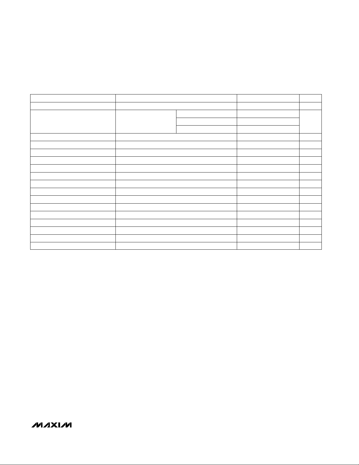
♦ Available in 20-Pin SSOP
20
19
18
17
16
15
14
13
1
2
3
4
5
6
7
8
LX
PGND
LX
PGND
IN
LX
IN
LX
TOP VIEW
LX
PGND
V
CC
COMPFBSEL
IN
LX
12
11
9
10
REF
GNDFB
TOFF
MAX1623
SSOP
SHDN
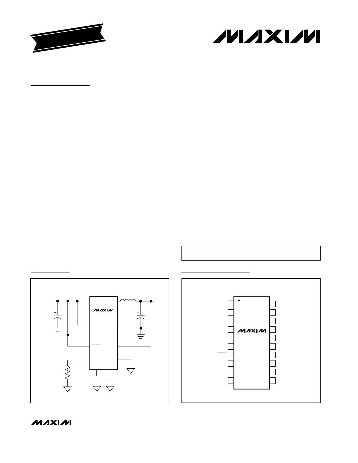
Pin Configuration
5V
INPUT
MAX1623
2.5V
OUTPUT
IN LX
PGND
GND
FB
REFCOMP
FBSEL
V
CC
TOFF
SHDN
Typical Operating Circuit
19-1436; Rev 2; 3/02
PART
MAX1623EAP -40°C to +85°C
TEMP RANGE PIN-PACKAGE
20 SSOP
Ordering Information
Idle Mode is a trademark of Maxim Integrated Products.
For pricing, delivery, and ordering information, please contact Maxim/Dallas Direct! at
1-888-629-4642, or visit Maxim’s website at www.maxim-ic.com.
Page 2

MAX1623
3A, Low-Voltage, Step-Down Regulator with
Synchronous Rectification and Internal Switches
2 _______________________________________________________________________________________
ABSOLUTE MAXIMUM RATINGS
ELECTRICAL CHARACTERISTICS
(VIN= VCC= 5V, FBSEL unconnected, R
TOFF
= 110kΩ, TA= 0°C to +85°C, unless otherwise noted. Typical values are at
T
A
= +25°C.)
Stresses beyond those listed under “Absolute Maximum Ratings” may cause permanent damage to the device. These are stress ratings only, and functional
operation of the device at these or any other conditions beyond those indicated in the operational sections of the specifications is not implied. Exposure to
absolute maximum rating conditions for extended periods may affect device reliability.
IN to PGND .....................................................................0V to 6V
V
CC
to GND ................................................................-0.3V to 6V
PGND to GND.....................................................................±0.5V
IN to V
CC
.............................................................................±0.5V
LX Current (Note 1).............................................................±5.5A
SHDN to GND .............................................................-0.3V to 6V
REF, FBSEL, COMP, FB, TOFF to GND .....-0.3V to (V
CC
+ 0.3V)
REF Short to GND ......................................................Continuous
Continuous Power Dissipation (T
A
= +70°C) (with part mounted
on 1 sq. inch of one ounce copper)
20-Pin SSOP (derate 22mW/°C above +70°C) ................1.3W
Operating Temperature Range ...........................-40°C to +85°C
Storage Temperature Range .............................-65°C to +150°C
Lead Temperature (soldering, 10s) .................................+300°C
SHDN = GND or V
CC
FBSEL = REF
FBSEL = GND
VIN= 4.5V to 5.5V,
I
LOAD
= 0 to 3A
(Note 2)
FBSEL = GND, adjustable output mode, VFB= 1.2V
VCCfalling, 100mV hysteresis
I
LOAD
≥ 1.5A (Note 2)
VIN= 4.5V
SHDN = GND
VIN= 4.5V
FBSEL = GND or REF (Note 2)
I
REF
= 0
Does not include switching losses
I
REF
= -1µA to 10µA
CONDITIONS
V0.8
SHDN Input Low Voltage
µA-1 0.03 1
SHDN Input Current
2
%
1
AC Output Load Regulation
µs0.85 1.00 1.15Off-Time Default Period
µs0.5 4Off-Time Adjustment Range
kHz500Error-Amplifier Gain Bandwidth
nA-25 25FB Input Bias Current
V4.1 4.2 4.3Undervoltage Lockout Threshold
°C145Thermal Shutdown Threshold
µA0.5 10Shutdown Supply Current
µA400 525No-Load Supply Current
A1 1.25 1.5Idle Mode Threshold (Note 3)
2.49 2.525 2.550
V
3.296 3.330 3.366
V4.5 5.5Input Voltage Range
Output Voltage
kHz350Maximum Switching Frequency
mΩ60 100NMOS Switch On-Resistance
mΩ55 100PMOS Switch On-Resistance
A3.65 4.65Current-Limit Threshold
1.089 1.100 1.110
VV
REF
3.80Output Adjustment Range
V1.089 1.100 1.110Reference Output Voltage
mV1Reference Load Regulation
UNITSMIN TYP MAXPARAMETER
FBSEL = unconnected
FBSEL = V
CC
FBSEL = GND or REF
V2
SHDN Input High Voltage
VIN= 5.5V, VLX= 5.5V or 0 µA±20LX Leakage Current
A3.65RMS LX Output Current
Note 1: LX has internal clamp diodes to PGND and IN. Applications that forward bias these diodes should take care not to exceed
the IC’s package power dissipation limits.
Page 3
MAX1623
_______________________________________________________________________________________ 3
3A, Low-Voltage, Step-Down Regulator with
Synchronous Rectification and Internal Switches
ELECTRICAL CHARACTERISTICS
(VIN= VCC= 5V, FBSEL unconnected, R
TOFF
= 110kΩ, TA= -40°C to +85°C, unless otherwise noted.) (Note 4)
Note 2: Guaranteed by design, not production tested.
Note 3: Idle Mode threshold is defined as the transition point in the load-current range between Idle Mode and constant-off-time
operation.
Note 4: Specifications to -40°C are guaranteed by design, not production tested.
SHDN = GND or V
CC
VIN= 4.5V to 5.5V,
I
LOAD
= 0 to 3A
FBSEL = GND, adjustable output mode, VFB= 1.2V
VCCfalling, 100mV hysteresis
VIN= 4.5V
VIN= 5.5V, VLX= 5.5V or 0
SHDN = GND
VIN= 4.5V
V
FBSEL = GND or REF (Note 2)
I
REF
= 0
Does not include switching losses
CONDITIONS
V0.8
FBSEL = unconnected
SHDN Input Low Voltage
µA-1 1
FBSEL = V
CC
SHDN Input Current
FBSEL = GND or REF
2.2
SHDN Input High Voltage
µs0.85 1.25Off-Time Default Period
µs0.55 4Off-Time Adjustment Range
nA-50 50FB Input Bias Current
V4.0 4.3Undervoltage Lockout Threshold
µA-20 20LX Leakage Current
µA10Shutdown Supply Current
µA600No-Load Supply Current
2.450 2.550
V
3.234 3.366
V4.5 5.5Input Voltage Range
Output Voltage
Ω
0.1NMOS Switch On-Resistance
Ω
0.1PMOS Switch On-Resistance
A3.5 4.75Current-Limit Threshold
1.075 1.110
VV
REF
3.8Output Adjustment Range
V1.075 1.110Reference Output Voltage
UNITSMIN TYP MAXPARAMETER
Page 4
MAX1623
3A, Low-Voltage, Step-Down Regulator with
Synchronous Rectification and Internal Switches
4 _______________________________________________________________________________________
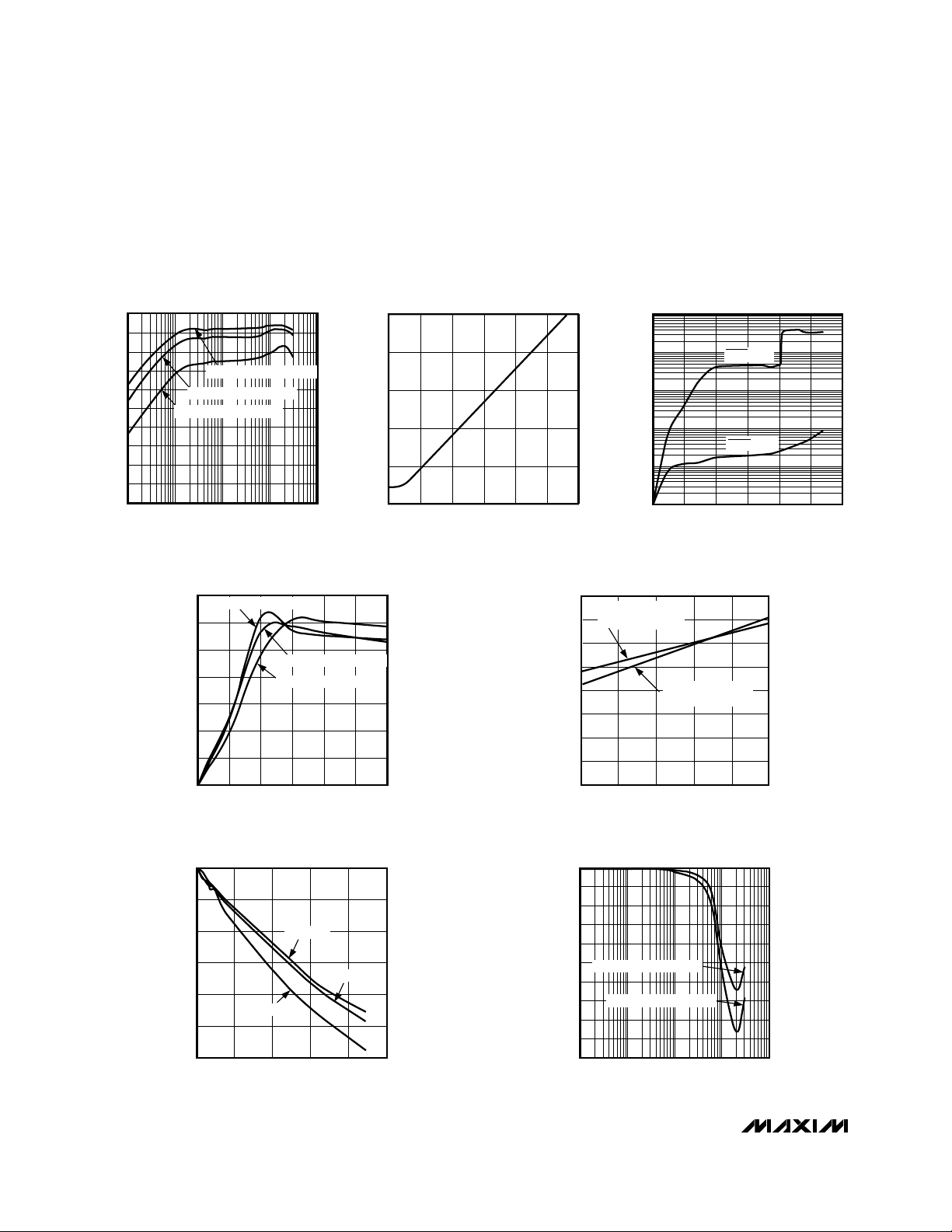
__________________________________________Typical Operating Characteristics
(Circuit of Figure 2, TA = +25°C, unless otherwise noted.)
100
0
0.001 0.1 10.01 10
EFFICIENCY
vs. OUTPUT CURRENT
20
MAX1623 TOC01
OUTPUT CURRENT (A)
EFFICIENCY (%)
40
60
80
90
10
30
50
70
V
OUT
= 3.3V, R
TOFF
= 110kΩ
V
OUT
= 1.1V, R
TOFF
= 280kΩ
V
OUT
= 2.5V, R
TOFF
= 180kΩ
0
1
3
2
4
5
0 200100 300 400 500 600
SWITCH OFF-TIME
vs. OFF-TIME RESISTANCE
MAX1623 TOC02
R
TOFF
(kΩ)
t
OFF
(µs)
1000
100
10
1
0.1
0.01
0123
4
56
SUPPLY CURRENT
vs. INPUT VOLTAGE
MAX1623 TOC03
INPUT VOLTAGE (V)
SUPPLY CURRENT (µA)
SHDN = IN
SHDN = GND
0
150
50
100
250
200
350
300
0 1000 1500500 2000 2500 3000
SWITCHING FREQUENCY
vs. LOAD CURRENT
MAX1623 TOC04
LOAD CURRENT (mA)
SWITCHING FREQUENCY (kHz)
V
OUT
= 2.5V, R
TOFF
= 180kΩ
V
OUT
= 3.3V, R
TOFF
= 110kΩ
V
OUT
= 1.1V, R
TOFF
= 280kΩ
0
200
150
100
50
300
250
350
400
4.5 4.94.7 5.1 5.3 5.5
SWITCHING FREQUENCY
vs. INPUT VOLTAGE
MAX1623 TOC05
INPUT VOLTAGE (V)
SWITCHING FREQUENCY (kHz)
VIN = 5V, V
OUT
= 3.3V,
R
TOFF
= 110kΩ
VIN = 5V, V
OUT
= 2.5V,
R
TOFF
= 180kΩ
0
-0.50
0.10.01 10.001 10
LOAD REGULATION ERROR
vs. LOAD CURRENT
-0.40
MAX1623 TOC07
LOAD CURRENT (A)
LOAD REGULATION ERROR (%)
-0.30
-0.20
-0.10
-0.35
-0.45
-0.25
-0.15
-0.05
V
OUT
= 2.5V, R
TOFF
= 180kΩ
V
OUT
= 3.3V, R
TOFF
= 110kΩ
-0.01
-0.02
-0.03
-0.04
-0.05
-0.06
0
0 5 10 15 20 25
REFERENCE LOAD REGULATION ERROR
vs. REFERENCE LOAD CURRENT
MAX1623 TOC06
REFERENCE LOAD CURRENT (µA)
REFERENCE LOAD REGULATION ERROR (%)
TA = +25°C
T
A
= -40°C
T
A
= +85°C
Page 5

MAX1623
_______________________________________________________________________________________ 5
3A, Low-Voltage, Step-Down Regulator with
Synchronous Rectification and Internal Switches
B
C
A
1ms/div
START-UP AND SHUTDOWN TRANSIENT
MAX1623 TOC08
VIN = 5V, V
OUT
= 3.3V, I
LOAD
= 3A,
WAVEFORM AVERAGED
A: V
OUT
, 2V/div
B: I
IN
, 1A/div
C: V
SHDN
, 5V/div
LOAD-TRANSIENT RESPONSE
(FBSEL = REF)
MAX1623 TOC10
I
LOAD
0 to 3A
V
OUT
50mV
AC-COUPLED
f = 300kHz
20µs/div
LINE-TRANSIENT RESPONSE
MAX1623 TOC12
VIN = 4.5V
to 5.5V
AC-COUPLED
(1V/div)
V
OUT
= 3.3V
AC-COUPLED
I
OUT
= 1.5A
(20mV/div)
20µs/div
LOAD-TRANSIENT RESPONSE
(FBSEL = REF)
MAX1623 TOC11
I
LOAD
0 to 2A
V
OUT
50mV
AC-COUPLED
f = 300kHz
20µs/div
____________________________ Typical Operating Characteristics (continued)
(Circuit of Figure 2, TA = +25°C, unless otherwise noted.)
LINE-TRANSIENT RESPONSE
MAX1623 TOC13
VIN = 4.5V
to 5.5V
AC-COUPLED
(1V/div)
V
OUT
= 3.3V
AC-COUPLED
I
OUT
= 100mA
(20mV/div)
20µs/div
B
C
A
1ms/div
START-UP AND SHUTDOWN TRANSIENT
MAX1623 TOC09
VIN = 5V, V
OUT
= 3.3V, I
LOAD
= 2A,
WAVEFORM AVERAGED
A: V
OUT
, 2V/div
B: I
IN
, 1A/div
C: V
SHDN
, 5V/div
Page 6
MAX1623
3A, Low-Voltage, Step-Down Regulator with
Synchronous Rectification and Internal Switches
6 _______________________________________________________________________________________
General Description
The MAX1623 current-mode, PWM, DC-DC regulator is
designed for 5V-input step-down applications. It features a 55mΩ (typ) PMOS switch and a 60mΩ (typ)
NMOS synchronous-rectifier switch. Simple constant-offtime control allows switching frequencies up to 350kHz.
Adjust the off-time with an external resistor R
TOFF
to
optimize performance trade-offs among efficiency, component size, output switching noise, and cost. Idle Mode
operation enhances light-load efficiency by switching to
a pulse-skipping mode that reduces transition and gatecharge losses. The power-switching circuit consists of
the IC and an LC output filter. The output voltage is the
average of the AC voltage at the switching node (LX).
The MAX1623 regulates the output voltage by changing
the PMOS switch on-time relative to the constant offtime, thereby adjusting the duty cycle.
The MAX1623 contains six major circuit blocks (Figure 1):
a PWM comparator, a current-sense circuit, a PWM
logic block, an internal feedback mux, an off-time control block, and a 1.1V precision reference. The input
supply directly powers the internal blocks.
Modes of Operation
The load current determines the mode of operation:
Idle Mode (load currents less than 0.625A) or PWM
mode for inductor currents of 1.25A (which corresponds to load currents greater than 0.625A). The
PWM current limit is continuously adjusted by the PWM
comparator and can vary from 0A to the maximum current limit (4A). If the inductor current falls below the Idle
Mode threshold (1.25A), skip mode takes over.
Whenever the P-channel switch turns on, it stays on
until the sensed current reaches the active current limit.
The PWM current limit automatically adjusts with the
PMOS switch duty cycle required to generate the
desired output voltage. When the active current limit is
met, the PMOS switch turns off for the programmed
minimum off-time, and the N-channel synchronous rectifier turns on. The synchronous rectifier stays on until
the P-channel switch turns back on or until the inductor
current reaches zero. At the end of the off-time, the Pchannel switch turns on again if the output voltage indicates that energy is required at the output.
Pin Description
NAME FUNCTION
1, 3, 5,
16,18, 20
LX Connection to the internal power switches.
2, 4, 6 IN Power Input. Internally connected to the PMOS switch source. Connect to 5V.
PIN
7
SHDN
Active-Low Shutdown Input. Connect to VCCfor normal operation.
8 FBSEL Feedback Select Input. See Table 1.
12 REF Reference Output. Bypass with a minimum 0.1µF capacitor to GND. See the Internal Reference section.
11 GND Analog Ground
10 FB
Feedback input for both fixed-output and adjustable operating modes. Connect to the output directly
for fixed-voltage operation or to a resistor-divider for adjustable operating modes.
9 TOFF
Off-Time Select Input. Connect a resistor from TOFF to GND to adjust the switch off-time, and therefore the frequency: t
OFF
= . See the Typical Operating Characteristics.
15, 17, 19 PGND Power Ground. Internally connected to the NMOS synchronous rectifier source.
14 V
CC
Analog Supply-Voltage Input. Supplies internal analog circuitry. Connect to 5V. Bypass VCCwith 10Ω
and 4.7µF (Figure 2).
13 COMP
Integrator Capacitor Connection. Connect a 470pF (470pF to 2000pF range) capacitor to GND to set
the typical integration time-constant. See the Integrator Amplifier section.
R
110k
s)
TOFF
Ω
(µ
Page 7

MAX1623
_______________________________________________________________________________________ 7
3A, Low-Voltage, Step-Down Regulator with
Synchronous Rectification and Internal Switches
Figure 1. Functional Diagram
Idle Mode
At light loads, the device goes into skip mode
(because the load current is below the skip threshold),
and Idle Mode operation (1.25A current limit) begins.
This allows both switches to remain off at the end of the
off-time, skipping cycles to reduce switching losses. At
lighter loads, the inductor current is discontinuous
because the inductor current reaches zero. In Idle
Mode, the operating frequency varies with output load
current. There is no major shift in circuit behavior as the
PWM limit falls below the skip limit. The effective offtime simply increases, resulting in a seamless transition
between PWM mode and Idle Mode.
PWM Mode
PWM operation occurs whenever the load current is
greater than the skip threshold. In this mode, the PWM
comparator adjusts the current limit to the desired output current, so that the P-channel turns on at the end of
each off-time.
Three signals are resistively summed at the input of the
PWM comparator (Figure 1): an output voltage error
signal relative to the reference voltage, an integrated
output voltage error correction signal, and the sensed
PMOS switch current. The integrated error signal is
provided by a transconductance amplifier with an
external capacitor at the COMP pin. This integrator provides high DC accuracy without the need for a highgain error amplifier. Connecting a capacitor at COMP
modifies the overall loop response (see the Integrator
Comparator section).
Setting the Output Voltage
There are two preset output voltages (2.525V and
3.33V), or the output voltage can be adjusted from the
reference voltage (nominally 1.1V) up to 3.8V. For a
preset output voltage (Figure 2), connect FB to the output voltage, and connect FBSEL to VCC(2.525V output) or leave it unconnected (3.33V output). For an
adjustable output, connect FBSEL to GND or REF, and
connect FB to the midpoint of a resistor divider
between the output voltage and ground (Figure 3).
Regulation is maintained when V
FB
equals V
REF
. Select
R1 in the 10kΩ to 500kΩ range. R2 is given by:
where V
REF
is typically 1.1V.
V
IN
4.5V TO
5.5V
FBSEL
FEEDBACK
SELECTION
IN
FB
COMP
V
IN
NOTE: HEAVY LINES DENOTE HIGH SWITCHING CURRENT PATHS.
V
SHDN
REF
CC
REF
G
m
REF
MAX1623
REF
GND
CURRENT
SENSE
SKIP
PWM LOGIC
AND
DRIVERS
LX
TIMER
TOFF
CURRENT
SENSE
PGND
R2 (R1)(V / V 1)
=−
OUT REF
Page 8

MAX1623
3A, Low-Voltage, Step-Down Regulator with
Synchronous Rectification and Internal Switches
8 _______________________________________________________________________________________
Setting the AC Loop Gain
The internal integrator amplifier effectively eliminates any
long-term error within the time constant set by the Gmof
the transconductance amplifier and the capacitor connected to COMP. However, there remains a short-term
load-regulation error in response to load current
changes. Proper FBSEL connection selects the relative
level of current feedback to voltage feedback, which
results in an AC load-regulation error of either 1% or 2%
of the output voltage (Table 1). The 2% setting is automatically selected in preset output voltage mode (FBSEL
connected to VCCor unconnected). This gain setting
minimizes the size and cost of the output filter capacitor
required. For extremely tight specifications that cannot
tolerate 2% short-term errors, connect FBSEL to ground
(adjustable mode) for 1% AC load regulation (see the
Input and Output Filter Capacitors (C1, C2) section).
Synchronous Rectification
Synchronous rectification improves efficiency by 3% to
5% at heavy loads when compared to a conventional
Schottky rectifier. To prevent cross-conduction or “shootthrough,” the synchronous rectifier turns on following a
short delay (dead time) after the P-channel power MOSFET turns off. In discontinuous (light-load) mode, the synchronous rectifier switch turns off as the inductor current
approaches zero. The synchronous rectifier works under
all operating conditions, including Idle Mode.
Integrator Amplifier (COMP)
An internal transconductance amplifier fine tunes the
output DC accuracy. The transconductance amplifier is
compensated at COMP. A capacitor from COMP to
ground determines the gain-bandwidth product and the
overall loop response. This integrator effectively eliminates any long-term error within the time constant set
by the G
m
of the transconductance amplifier and the
capacitor connected to COMP.
For stability, choose COMP as follows:
where G
m
= 9.1µS.
AC LOAD
REGULATION (%)
OUTPUT
VOLTAGE (V)
IN 2 2.525
Unconnected 2 3.33
FBSEL PIN
GND 1 Adjustable
V
REF
2 Adjustable
Figure 2. Standard 3.3V/3A Application Circuit
Table 1. Output Voltage Selection
INPUT
4.5V TO 5.5V
IN
10µF
4.7µH
220µF
3.3V OUTPUT
C1
C2
330µF
LX
MAX1623
PGND
10Ω
NOTE: HEAVY LINES
DENOTE HIGH SWITCHING
CURRENT PATHS.
4.7µF
SHDN
FBSEL
V
CC
FB
TOFF
COMP
REF
GND
0.1µF
110k
470pF
C
COMP
G R C
××
m LOAD OUT
≥
4
Page 9

A high capacitor value maintains a constant average
output voltage but slows the loop response to changes
in output voltage. A low capacitor value speeds up the
loop response to changes in output voltage. Choose
the capacitor value that results in optimal performance.
Current Limiting
The current-sense circuit enables when the PMOS
power switch is on. This circuit’s corresponding output
voltage feeds three separate comparators: the skip current comparator (1.25A), the maximum current comparator (4.15A), and the PWM current comparator (see
the Modes of Operation section).
Oscillator Frequency and
Programming the Off-Time
The MAX1623 features a programmable off-time that is
set by R
TOFF
connected from TOFF to GND. Connecting
a 110kΩ resistor from TOFF to GND achieves a 1µs
(nominal) off-time. The off-time is inversely proportional
to R
TOFF
according to the formula:
t
OFF
= R
TOFF
/ 110k (µs)
t
OFF
is adjustable between 0.5µs to 4µs (see the
Typical Operating Characteristics). To set the switching
frequency when the inductor operates in continuousconduction mode, the off-time has to be set to:
where:
t
OFF
= the programmed off-time
VI= input voltage
VO= output voltage
f = desired switching frequency during continuous
inductor current
V
PCH
= the voltage drop across the internal P-channel
switch
V
NCH
= the voltage drop across the internal N-channel
synchronous rectifier
Switching frequency decreases as load current is
decreased below the 625mA Idle Mode trip point.
Internal Reference
The 1.10V internal reference (available at REF) is accurate to ±1.5% over the -40°C to +85°C operating range,
making it useful as a precision system reference. Bypass
the reference to ground with a minimum 0.1µF ceramic
capacitor. For low noise and jitter performance, use a
0.47µF ceramic capacitor. The reference can supply up
to 10µA for external loads. However, if tight accuracy
specifications for either reference or the main output are
essential, avoid reference loads in excess of 5µA.
Loading the reference reduces the main output voltage
slightly, according to the reference-voltage load-regulation error.
Start-Up
To prevent the MAX1623 from false output regulation,
the internal PMOS and NMOS switches will not switch
on until all of the following conditions are true: the supply voltage is above the undervoltage lockout threshold, SHDN is pulled high, the internal reference voltage
is at 75% of its nominal (1.1V) value, and the die temperature is below +145°C. When the above conditions
are satisfied, the MAX1623 will regulate the output voltage to the selected level. The MAX1623 typically starts
up in 1ms for full output load.
Thermal Shutdown and
Overload Conditions
Thermal overload protection limits the MAX1623’s total
power dissipation. When the junction temperature
reaches T
j
= +145°C, the device turns off, allowing it to
cool down. Switching resumes after the IC’s junction
temperature decreases by 20°C. If the thermal overload
condition persists, the output pulses on and off.
Thermal overload protection is designed to protect the
MAX1623 during fault conditions, such as an output
short circuit.
Thermal Resistance
Junction to ambient thermal resistance (θJA) strongly
depends on the amount of copper area immediately
surrounding the IC’s leads. The MAX1623 evaluation kit
has 0.8in2of copper area. θJAon this board was measured to have 45°C/W of thermal resistance with no air
MAX1623
_______________________________________________________________________________________ 9
3A, Low-Voltage, Step-Down Regulator with
Synchronous Rectification and Internal Switches
Figure 3. Adjustable Output Voltage
LX
MAX1623
PGND
GND
FB
R1 = 10kΩ to 500kΩ
R2 = R1(V
OUT
= 1.1V
V
REF
/ V
- 1)
REF
V
OUT
R2
R1
t
=
OFF
−−
VV V
I O PCH
−
fV V V
( )
I PCH NCH
+
Page 10
MAX1623
3A, Low-Voltage, Step-Down Regulator with
Synchronous Rectification and Internal Switches
10 _______________________________________________________________________________________
flow. A copper area of 0.4in2showed thermal resistance of 60°C/W.
Airflow over the IC can significantly reduce θJA.
Power Dissipation
The MAX1623’s power dissipation consists mostly of conduction losses in the two internal power switches. Power
dissipation due to supply current in the control section
and average current used to charge and discharge the
gate capacitance of the two power switches is less than
30mW at 300kHz. This number is reduced when switching frequency is reduced as the part enters Idle Mode.
Combined conduction loss in the two power switches is
calculated by:
PD= I
LOAD
2
(RON)
where RON= 100mΩ (max).
The θJArequired to deliver this amount of power is cal-
culated by:
θJA= (T
J(MAX)
– T
A(MAX)
) / P
D
where:
T
J(MAX)
= maximum allowed junction temperature
T
A(MAX)
= maximum ambient temperature expected
Applications Information
Inductor L1
The inductor value can be adjusted to optimize the
design for size, cost, and efficiency. Three key inductor
parameters must be specified: inductance value (L),
peak current (I
PEAK
), and DC resistance (RDC). The following equation includes a constant, denoted as LIR,
which is the ratio of inductor peak-to-peak AC current
to DC load current. A higher value of LIR allows smaller
inductance, but results in higher losses and ripple. A
good compromise between size and losses is found at
a 30% ripple current to load current ratio (LIR = 0.3),
which corresponds to a peak inductor current 1.15
times the DC load current:
where:
f = switching frequency
I
OUT
= maximum DC load current
LIR = ratio of AC to DC inductor current, typically
0.3
The peak inductor current at full load is 1.15 x I
OUT
if
the above equation is used; otherwise, the peak current
can be calculated by:
The inductor’s DC resistance is a key parameter for efficiency and must be minimized, preferably to less than
25mΩ at I
OUT
= 3A. To reduce EMI, use a shielded
inductor.
Input and Output Filter
Capacitors (C1, C2)
Use a low-ESR input capacitor according to the input
ripple-current requirements and voltage rating.
In addition to C1, place a 10µF ceramic bypass capacitor
from the power input (pin 2, 4, 6) to power ground (pin
15, 17, 19) within 5mm of the IC.
The output filter capacitor determines the output voltage ripple and output load-transient response, as well
as the loop’s stability.
The output ripple in continuous-conduction mode is:
where f is the switching frequency.
Table 2. Suggested Values (VIN= 5V,
IO= 3A, f = 300kHz)
T
OFF
(µs)
L
(µH)
3.3 1.10 4.7
2.5 1.67 4.7
V
OUT
(V)
1.8 2.16 4.7
1.5 2.38 3.9
1.1 2.68 3.3
R
TOFF
(kΩ)
120
180
240
260
280
L
V(V V)
OUT IN(MAX) OUT
=
V f (I ) (LIR)
IN(MAX) OUT
××
−
V(V V)
II
=+
PEAK OUT
OUT IN(MAX) OUT
2 f L V
II
RIPPLE LOAD
=
V I LIR ESR
OUT(RPL) OUT(MAX) C2
=× +
−
×× ×
IN(MAX)
××
π
1
VVV
−
()
OUT IN OUT
V
IN
2 f C2
Page 11

Loop Stability
Stable operation requires the right output filter capacitor. When choosing the output capacitor, ensure the following conditions are met:
and
10mΩ≤R
ESR
Circuit Layout and Grounding
Good layout is necessary to achieve the intended output power level, high efficiency, and low noise. Good
layout includes the use of a ground plane, appropriate
component placement, and correct routing of traces
using appropriate trace widths. For heatsinking purposes, copper area connected at the IC should be evenly
distributed among the high-current pins.
1) Minimize high-current ground loops. Connect the
input capacitor’s ground, output capacitor’s
ground, and IC PGND together.
2) A ground plane is essential for optimum performance. In most applications, the circuit will be
located on a multilayer board, and full use of the
four or more copper layers is recommended. Use
the top and bottom layers for interconnections and
the inner layers for an uninterrupted ground plane.
3) Place the LX node components as close together
as possible. This reduces resistive and switching
losses and confines noise due to ground inductance.
4) Connect the input filter capacitor less than 10mm
away from IN. The connecting copper trace carries
large currents and must be at least 2mm wide,
preferably 5mm.
5) Connect GND directly to PGND at only one point
near the IC.
MAX1623
______________________________________________________________________________________ 11
3A, Low-Voltage, Step-Down Regulator with
Synchronous Rectification and Internal Switches
___________________Chip Information
TRANSISTOR COUNT: 1220
C80t
≥× ×
2 OFF
V
V
OUT
REF
Page 12
MAX1623
3A, Low-Voltage, Step-Down Regulator with
Synchronous Rectification and Internal Switches
Maxim cannot assume responsibility for use of any circuitry other than circuitry entirely embodied in a Maxim product. No circuit patent licenses are
implied. Maxim reserves the right to change the circuitry and specifications without notice at any time.
12 ____________________Maxim Integrated Products, 120 San Gabriel Drive, Sunnyvale, CA 94086 408-737-7600
© 2002 Maxim Integrated Products Printed USA is a registered trademark of Maxim Integrated Products.
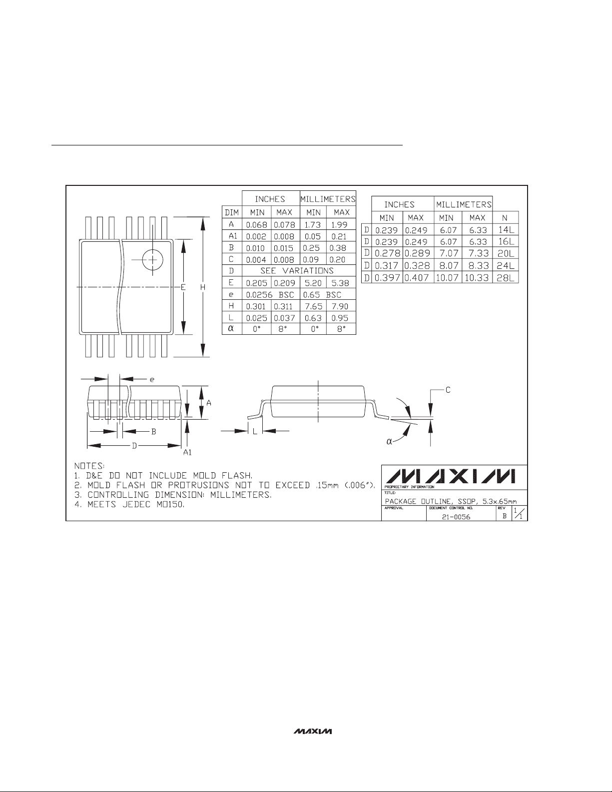
Package Information
(The package drawing(s) in this data sheet may not reflect the most current specifications. For the latest package outline information,
go to www.maxim-ic.com/packages.)
SSOP.EPS
 Loading...