

Page 1
General Description
The MAX1620/MAX1621 convert a 1.8V to 20V battery
voltage to a positive or negative LCD backplane bias
voltage. Backplane bias voltage can be automatically
disabled when the display logic voltage is removed,
protecting the display. These devices use very little PC
board area, come in ultra-small QSOP packages, and
require only small, low-profile external components.
Output voltage can be set to a desired positive or negative voltage range with external resistors, and adjusted
over that range with the on-board digital-to-analog converter (DAC) or with a potentiometer. The MAX1620/
MAX1621 include a 5-bit DAC, allowing digital software
control of the bias voltage. The MAX1620 uses up/down
digital signaling to adjust the DAC, and the MAX1621
uses the System Management Bus (SMBus™) 2-wire
serial interface.
These devices use a low-cost, external, N-channel MOSFET
power switch or NPN transistor, and can be configured
for positive or negative output voltages. Operating current is a low 150µA, typically provided from a display’s
logic supply of 3.0V to 5.5V. The MAX1620/MAX1621 are
available in a 16-pin QSOP package.
Applications
Notebook Computers
Palmtop Computers
Personal Digital Assistants
Portable Data-Collection Terminals
Features
♦ 1.8V to 20V Battery Input Voltage
♦ Automatic Disable when Display Logic
is Shut Down
♦ Extremely Small QSOP Package
♦ 32-Level Internal DAC
♦ SMBus Serial Interface (MAX1621)
♦ Positive or Negative Output Voltage
MAX1620/MAX1621
Digitally Adjustable LCD Bias Supplies
________________________________________________________________
Maxim Integrated Products
1
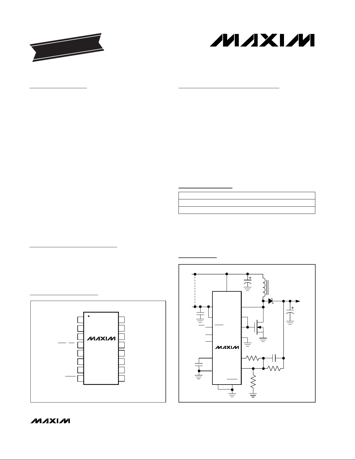
PART
MAX1620EEE
MAX1621EEE
-40°C to +85°C
-40°C to +85°C
TEMP. RANGE PIN-PACKAGE
16 QSOP
16 QSOP
EVALUATION KIT MANUAL
FOLLOWS DATA SHEET
Ordering Information
19-1214; Rev 1; 1/98
LX
DHI
DLO
PGND
DOUT
FB
V
DD
POL
SHDN
DN
UP
REF
AGND
MAX1620
12.5V
TO
23.5V OUT
2V TO
12V
3V TO
5.5V
ON
/
OFF
DOWN
UP
LCDONPOK
BATT
Typical Operating Circuit
SMBus is a trademark of Intel Corp.
Pin Configuration
16
15
14
13
12
11
10
9
1
2
3
4
5
6
7
DHI
DLO
LX
PGND
AGND
V
DD
DOUT
FB
DN (SDA)
UP (SCL)
BATT
SHDN (SUS)
POK
REF
POL
LCDON
TOP VIEW
MAX1620
MAX1621
QSOP
( ) ARE FOR MAX1621 ONLY.
8
For free samples & the latest literature: http://www.maxim-ic.com, or phone 1-800-998-8800.
For small orders, phone 1-800-835-8769.
Page 2
MAX1620/MAX1621
Digitally Adjustable LCD Bias Supplies
2 _______________________________________________________________________________________
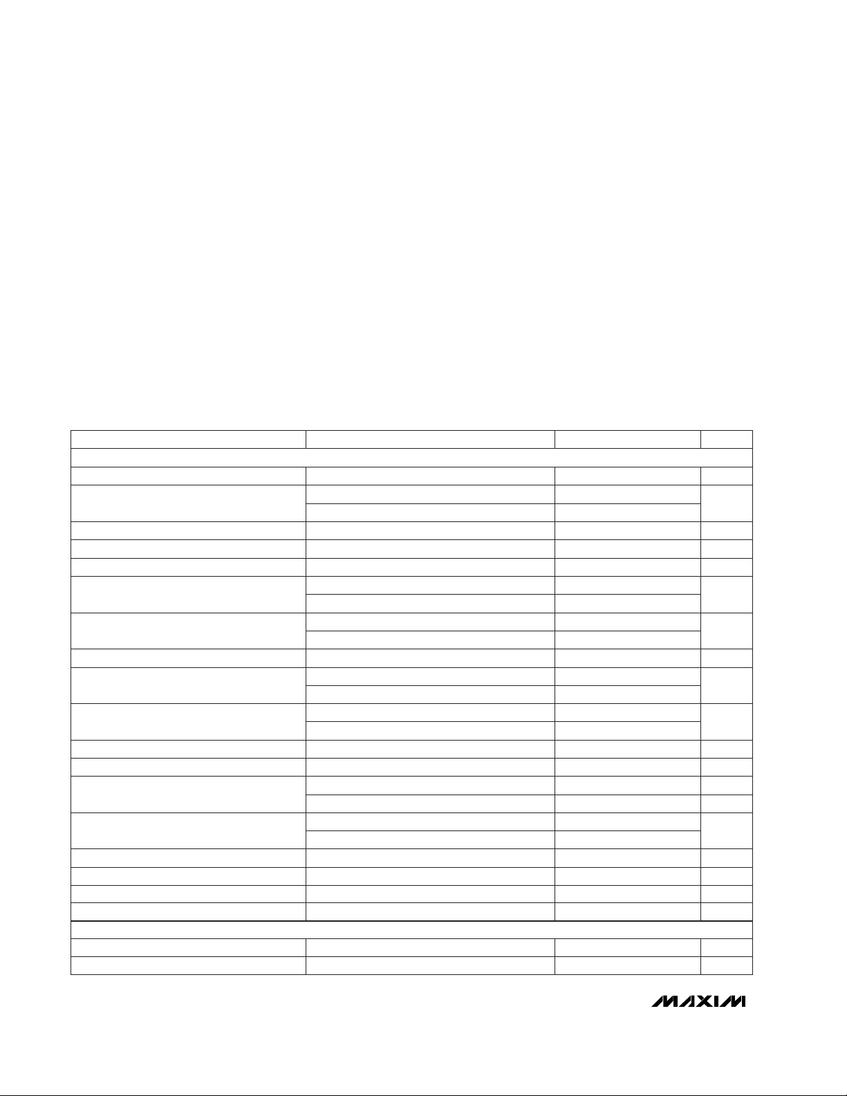
ABSOLUTE MAXIMUM RATINGS
ELECTRICAL CHARACTERISTICS
(VDD= 3.3V, V
BATT
= 10V, TA= 0°C to +85°C, unless otherwise noted.)
Stresses beyond those listed under “Absolute Maximum Ratings” may cause permanent damage to the device. These are stress ratings only, and functional
operation of the device at these or any other conditions beyond those indicated in the operational sections of the specifications is not implied. Exposure to
absolute maximum rating conditions for extended periods may affect device reliability.
VDDto AGND..............................................................-0.3V to 6V
PGND to AGND ..................................................................±0.3V
BATT, LX,
LCDON to AGND....................................-0.3V to 30V
DHI, DLO to PGND.....................................-0.3V to (V
DD
+ 0.3V)
DOUT, FB, POL, POK, REF to AGND.........-0.3V to (V
DD
+ 0.3V)
UP, DN, SHDN to AGND.............................................-0.3V to 6V
SCL, SDA, SUS to AGND............................................-0.3V to 6V
I
DHI
......................................................................................60mA
I
DLO
....................................................................................-30mA
I
LCDON
...............................................................................-10mA
Continuous Power Dissipation (T
A
= +70°C)
QSOP (derate 8.3mW/°C above +70°C) ......................667mW
Operating Temperature Range
MAX1620EEE/MAX1621EEE ............................-40°C to +85°C
Storage Temperature Range.............................-65°C to +150°C
Lead Temperature (soldering, 10sec).............................+300°C
V
LCDON
= 28V, POK = 0.967V
V
LCDON
= 0.4V, POK = 1.017V
FB = -50mV
FB = REF + 100mV
POL = AGND, 3.0V ≤ V
DD
≤ 5.5V
Shutdown mode, V
SHDN
= VDD,VDD= 5.5V
POL = VDD, 3.0V ≤ V
DD
≤ 5.5V
Operating mode, output in regulation, VDD= 5.5V
VDD= 5V
VDD= 5V
VDD= 3.0V
LX = 12V, shutdown mode
VDD= 4.5V
LX = 12V, operating mode
BATT = 12V, shutdown mode
4V ≤ BATT ≤ 12V, TA= 0°C to +85°C
BATT = 12V, operating mode
1.8V ≤ BATT ≤ 20V, TA= +25°C
µA1
LCDON High, Leakage Current
mA-2 -6
LCDON Low, Sinking Current
nA
-10 85
-20 10
FB Input Current (Note 3)
mV-8 0 8
V1.46 1.5 1.53
FB Regulation Voltage
mA-25DLO Output Current (Note 3)
mA50DHI Output Current (Note 3)
Ω
14
7
On-Resistance (DLO, DHI)
16.5 23.5
µs-V
20
Microsecond-Volt Time Constant (k-factor)
V27Positive Output Voltage
920
µA
150 250
VDDSupply Current
1.8 20BATT Operating Range (Note 2)
1
µA
13 20
LX Input Current
µA
1
BATT Input Current
-27Negative Output Voltage
V1.5 2.8Undervoltage Lockout Threshold (Note 1)
13 20
V3.0 5.5VDDOperating Range
Voltage on POK rising V0.967 0.992 1.017POK Threshold Voltage
V
mV12POK Hysteresis
CONDITIONS UNITS
MIN TYP MAX
PARAMETER
V
No load V1.47 1.5 1.53REF Voltage
0µA ≤ I
REF
≤ 25mA mV310REF Load Regulation
SWITCHING REGULATOR
REFERENCE AND DAC OUTPUT
Page 3

MAX1620/MAX1621
Digitally Adjustable LCD Bias Supplies
_______________________________________________________________________________________
3
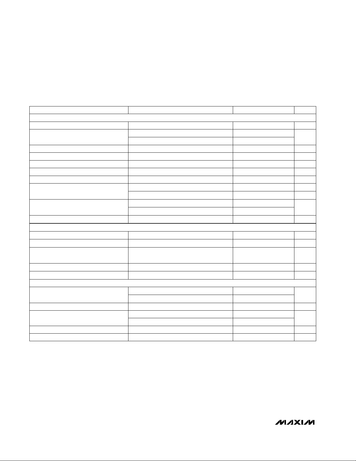
ELECTRICAL CHARACTERISTICS (continued)
(VDD= 3.3V, V
BATT
= 10V, TA= 0°C to +85°C, unless otherwise noted.)
TIMING CHARACTERISTICS
(TA= 0°C to +85°C, unless otherwise noted.)
-20µA ≤ I
DOUT
≤ 0µA
I
SDA
= -6mA
VIN= 0V or VIN= V
DD
VDD= 5.5V
VDD= 5.5V
3.0V ≤ VDD≤ 3.6V
3.0V ≤ VDD≤ 3.6V
48.39mV step size
VIN= 0V or VIN= V
DD
Guaranteed monotonic
0µA ≤ I
DOUT
≤ 40µA
V0.4
µA±1
SCL, SDA, SUS Input Leakage Current
V0.6
SCL, SDA, SUS Input Low Voltage
V
2.3
1.4
SCL, SDA, SUS Input High Voltage
±1
V
0.6
V0 0.007DOUT Minimum Output Voltage (Note 3)
2.3
V
1.4
UP, DN, SHDN, POL Input High Voltage
LSBDOUT Differential Nonlinearity
Bits5DOUT Resolution
±1
REF - REF +
0.02 0.02
DOUT Maximum Output Voltage (Note 3) V
UP, DN, SHDN, POL Input Leakage Current
µA
UP, DN, SHDN, POL Input Low Voltage
SDA Output Low Voltage
CONDITIONS UNITSMIN TYP MAXPARAMETER
DIGITAL INPUTS AND OUTPUTS
(Note 4)
(Note 4)
(Note 4)
CONDITIONS
1
SCL Falling Edge to SDA Valid
Master Clocking in Data
µst
DV
µs4t
HD:STA
Start Condition SDA to SCL
Hold Time
µs4.7t
SU:STA
Start Condition SCL to SDA
Setup Time
µs4t
HIGH
SCL High Time
µs4.7t
LOW
SCL Low Time
ns300t
F
SCL/SDA Fall Time
µs1t
1
Pulse Width High (UP, DN)
µs1t
R
SCL/SDA Rise Time
ns0t
HD:DAT
SCL to SDA Data-Hold Time
ns500tSU:
DAT
SDA to SCL Data-Setup Time
µs1t
2
Pulse Width Low (UP, DN)
µs1t
3
Pulse Separation (UP, DN)
µs1t
4
Counter Reset Time
UNITSMIN TYP MAXSYMBOLPARAMETER
µs4t
SU:STO
Stop Condition SCL_ to SDA_
Setup Time
MAX1620 (Figure 1)
MAX1621 (Figures 2 and 3)
Page 4
MAX1620/MAX1621
Digitally Adjustable LCD Bias Supplies
4 _______________________________________________________________________________________
Operating mode, output in regulation
µA
150 250
0µA ≤ I
REF
≤ 25µA
No load
REF Load Regulation
Voltage on POK rising
V
POL = VDD, 3.0V ≤ V
DD
≤ 5.5V
FB = 0V - 50mV
3.0 5.5
4V ≤ BATT ≤ 12V
VDDOperating Range
FB = REF + 100mV
POL = AGND, 3.0V ≤ V
DD
≤ 5.5V
mV510
V1.44 1.5 1.56REF Voltage
V27Positive Output Voltage
0.957 0.992 1.027
Shutdown mode, V
SHDN
= V
DD
20
-10 120
FB Input Current (Note 3)
VDDSupply Current
V
-30 10
mV-10 0 10
V1.5 2.8Undervoltage Lockout Threshold (Note 1)
nA
1.44 1.5 1.56
µs-VMicrosecond-Volt Time Constant (k-factor) 16 24
V1.8 20BATT Operating Range (Note 2)
-27Negative Output Voltage
FB Regulation Voltage
V
POK Threshold Voltage
DOUT Maximum Output Voltage (Note 3) V
REF - REF +
0.02 0.02
0µA ≤ I
DOUT
≤ 40µA
-20µA ≤ I
DOUT
≤ 0µADOUT Minimum Output Voltage (Note 3) V0 0.01
Guaranteed monotonicDOUT Differential Nonlinearity LSB±1
UP, DN, SHDN, POL Input High Voltage
3.0V ≤ VDD≤ 3.6V 1.4
VDD= 5.5V 2.3
V
UP, DN, SHDN, POL Input Low Voltage
0.6 V
3.0V ≤ VDD≤ 3.6V 1.4
VDD= 5.5V 2.3
SCL, SDA, SUS Input Low Voltage
0.6 V
SDA Output Low Voltage I
SDA
= -6mA 0.4 V
CONDITIONS UNITS
MIN TYP MAX
PARAMETER
ELECTRICAL CHARACTERISTICS
(VDD= 3.3V, V
BATT
= 10V, TA= -40°C to +85°C. Typical values are at TA= +25°C, unless otherwise noted. Limits over this
temperature range are guaranteed by design.)
V
SCL, SDA, SUS Input High Voltage
V
SWITCHING REGULATOR
REFERENCE AND OUTPUT
DIGITAL INPUTS AND OUTPUTS
Page 5
MAX1620/MAX1621
Digitally Adjustable LCD Bias Supplies
_______________________________________________________________________________________ 5
TIMING CHARACTERISTICS
(VDD= 3.3V, V
BATT
= 10V, TA= -40°C to +85°C. Typical values are at TA= +25°C, unless otherwise noted. Limits over this
temperature range are guaranteed by design.)
CONDITIONS
4
Stop Condition SCL_ to SDA_
Setup Time
µst
SU:STO
µs4t
HD:STA
Start Condition SDA_ to SCL_
Hold Time
µs4.7t
SU:STA
Start Condition SCL_ to SDA_
Setup Time
µs4t
HIGH
SCL High Time
µs4.7t
LOW
SCL Low Time
ns300t
F
SCL/SDA Fall Time
µs1t
1
Pulse Width High (UP, DN)
µs1t
R
SCL/SDA Rise Time
ns0t
HD:DAT
SCL_ to SDA_ Data-Hold Time
ns500tSU:
DAT
SDA_ to SCL_ Data-Setup Time
µs1t
2
Pulse Width Low (UP, DN)
µs1t
3
Pulse Separation (UP, DN)
µs1t
4
Counter Reset Time
UNITSMIN TYP MAXSYMBOLPARAMETER
Note 1: The setting in the DAC is guaranteed to remain valid as long as VDDis greater than the UVLO threshold.
Note 2: BATT Operating Range is guaranteed by the Microsecond-Volt Time Constant specification.
Note 3: Current sourced from a pin is denoted as positive current. Current sunk into a pin is denoted as negative current.
Note 4: Guaranteed by design.
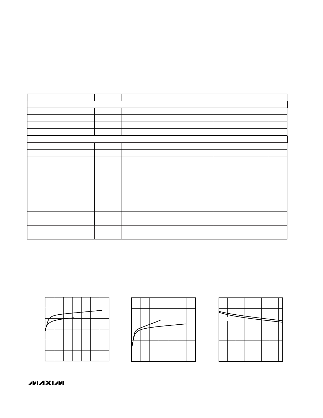
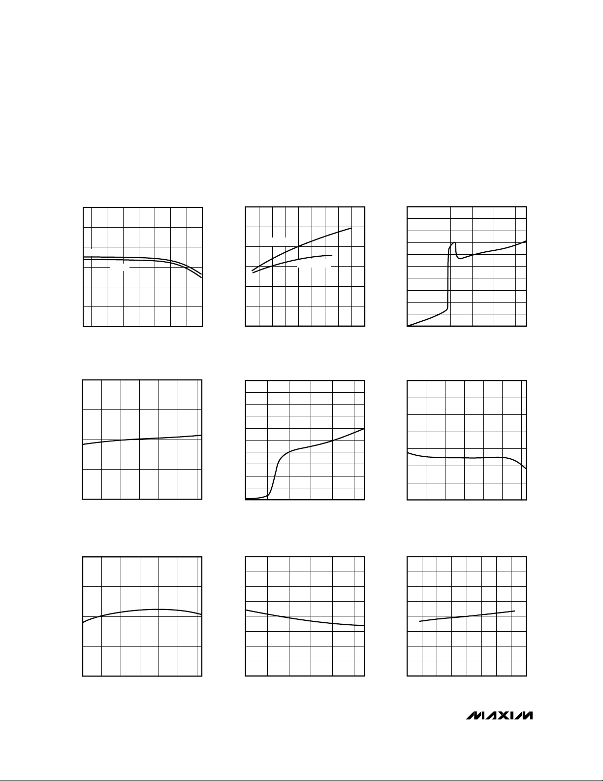
__________________________________________Typical Operating Characteristics
(VDD= 5V, V
BATT
= 10V, L1 = 100µH, TA= +25°C, unless otherwise noted.)
0.70
0.75
0.80
0.85
0.90
0.95
1.00
010203040506070
EFFICIENCY vs. OUTPUT CURRENT
MAX1620/21-01
OUTPUT CURRENT (mA)
EFFICIENCY (%)
+25V
+15V
0.70
0.75
0.80
0.85
0.90
0.95
1.00
010203040506070
EFFICIENCY vs. OUTPUT CURRENT
MAX1620/21-02
OUTPUT CURRENT (mA)
EFFICIENCY (%)
-25V
-15V
0.70
0.75
0.80
0.85
0.90
0.95
1.00
12 14 16 18 20 22 24 26
EFFICIENCY vs. OUTPUT VOLTAGE
MAX1620/21-03
OUTPUT VOLTAGE (V)
EFFICIENCY (%)
+10mA
+20mA
1
SCL Falling Time to SDA Valid
Master Clocking in Data
µst
DV
MAX1620 (Figure 1)
MAX1621 (Figures 2 and 3)
Page 6
MAX1620/MAX1621
Digitally Adjustable LCD Bias Supplies
6 _______________________________________________________________________________________
_____________________________Typical Operating Characteristics (continued)
(V
DD
=
5V, V
BATT
= 10V, L1 = 100µH, TA= +25°C, unless otherwise noted.)
0.70
0.75
0.80
0.85
0.90
0.95
1.00
-26 -24 -22 -20 -18 -16 -14 -12
EFFICIENCY vs. OUTPUT VOLTAGE
MAX1620/21-04
OUTPUT VOLTAGE (V)
EFFICIENCY (%)
-10mA
-20mA
0.70
0.75
0.80
0.85
0.90
0.95
1.00
2 4 6 8 10 12 14 16 18 20
EFFICIENCY vs. V
BATT
MAX1620/21-05
V
BATT
(V)
EFFICIENCY (%)
+20V, +10mA
-20V, -10mA
0
20
40
60
80
100
120
140
160
180
200
012345
SUPPLY CURRENT
vs. SUPPLY VOLTAGE
MAX1620/21-06
SUPPLY VOLTAGE (V)
SUPPLY CURRENT (µA)
100
125
150
175
200
-40 -20 0 20 40 60 80
SUPPLY CURRENT vs. TEMPERATURE
MAX1620/21-07
TEMPERATURE (°C)
SUPPLY CURRENT (µA)
1.49
1.50
1.51
-40 -20 0 20 40 60 80
REFERENCE VOLTAGE
vs. TEMPERATURE
MAX1620/21-10
TEMPERATURE (°C)
REFERENCE VOLTAGE (V)
0
2
4
6
8
10
12
14
16
18
20
012345
SHUTDOWN SUPPLY CURRENT
vs. SUPPLY VOLTAGE
MAX1620/21-08
SUPPLY VOLTAGE (V)
SUPPLY CURRENT (µA)
6
8
10
12
14
16
18
20
-40 -20 0 20 40 60 80
SHUTDOWN SUPPLY CURRENT
vs. TEMPERATURE
MAX1620/21-09
TEMPERATURE (°C)
SUPPLY CURRENT (µA)
18.0
18.5
19.0
19.5
20.0
20.5
21.0
21.5
22.0
2.5 3.0 3.5 4.0 4.5 5.0
k-FACTOR vs. SUPPLY VOLTAGE
MAX1620/21-11
SUPPLY VOLTAGE (V)
k-FACTOR (µs-V)
18.0
18.5
19.0
19.5
20.0
20.5
21.0
21.5
22.0
-60 -40 -20 0 20 40 60 80 100
k-FACTOR vs. TEMPERATURE
MAX1620/21-12
TEMPERATURE (°C)
k-FACTOR (µs-V)
Page 7

MAX1620/MAX1621
Digitally Adjustable LCD Bias Supplies
_______________________________________________________________________________________ 7
15
16
17
18
19
20
21
22
23
24
25
0 5 10 15 20
k-FACTOR vs. V
BATT
MAX1620/21-13
V
BATT
(V)
k-FACTOR (µs-V)
LINE-TRANSIENT RESPONSE
V
OUT
(AC COUPLED, 5mV/div)
V
DD
(AC COUPLED, 1V/div)
I
LOAD
= 20mA
2ms/div
5.3V
3.3V
MAX1620/21-14
LOAD-TRANSIENT RESPONSE
V
OUT
(AC COUPLED, 20mV/div)
I
OUT
(10mA/div)
20mA
0
I
LOAD
= 0mA TO 20mA
2ms/div
MAX1620/21-15
_____________________________Typical Operating Characteristics (continued)
(V
DD
=
5V, V
BATT
= 10V L1 = 100µH, V
OUT
= 22.3V, TA= +25°C, unless otherwise noted.)
Page 8
MAX1620/MAX1621
Digitally Adjustable LCD Bias Supplies
8 _______________________________________________________________________________________
External Transistor Drive, HighDHI1616
External Transistor Drive, LowDLO1515
Switching-Voltage Sense InputLX1414
Power GroundPGND1313
Analog GroundAGND1212
IC Input Supply, 3.0V to 5.5VV
DD
1111
DAC Output Voltage
Logic-Level Shutdown Input (active-low)
System Management Bus Suspend-Mode Input (active-low)
Power OK Voltage-Sense Input, 1V threshold
Reference Voltage Output. Bypass REF with 0.1µF to AGND.
Logic-Level Input. POL selects output voltage polarity: high = positive boost,
low = negative boost.
Logic-Level Input. A rising edge on UP increases V
OUT
.UP = DN = high resets
the counter to mid-scale.
DOUT
System Management Bus Serial-Clock Input
Battery Voltage-Sense Input
System Management Bus Serial-Data Input and Open-Drain Output
10
Logic-Level Input. A rising edge on DN decreases V
OUT
.UP = DN = high resets
the counter to mid-scale.
10
FUNCTION
SHDN
—4
SUS
4—
POK55
REF66
POL77
UP—2
Feedback Voltage InputFB9
SCL2—
BATT33
SDA1—
9
Open-Drain Output. LCDON controls LCD with external PNP.LCDON
8
DN—1
8
MAX1621MAX1620
NAME
PIN
______________________________________________________________Pin Description
Page 9

MAX1620/MAX1621
Digitally Adjustable LCD Bias Supplies
_______________________________________________________________________________________ 9
t
3
t
1
UP
DN
t
2
t
4
Figure 1. MAX1620 UP and DN Signal Timing
Figure 2. MAX1621 SMB Serial-Interface Timing—Address
Figure 3. MAX1621 SMB Serial-Interface Timing—Acknowledge
MOST SIGNIFICANT
CLOCKED INTO SLAVE
SCL
START
CONDITION
ADDRESS BIT (A6)
A5 CLOCKED
INTO SLAVE
A4 CLOCKED
INTO SLAVE
A3 CLOCKED
INTO SLAVE
t
HD:STA
SDA
t
SU:STA
t
SU:DAT
RW BIT
CLOCKED
INTO SLAVE
SCL
• • •
SDA
• • •
t
HD:DAT
t
LOW
ACKNOWLEDGED
BIT CLOCK
INTO MASTER
SLAVE PULLING
t
DV
SDA LOW
t
SU:DAT
MOST SIGNIFICANT
BIT CLOCKED
t
DV
t
HD:DAT
t
HIGH
t
SU:STO
Page 10

MAX1620/MAX1621
Digitally Adjustable LCD Bias Supplies
10 ______________________________________________________________________________________
R1
360k
2V
TO
12V
BATT
POK
D1
MBRS0540
N1
MMFT3055VL
Q1
MMBT2907
V
DD
POL
SHDN (SUS)
DN (SDA)
UP (SCL)
REF
AGND
3
5
OPTIONAL
11
7
4
1
2
6
12
( ) ARE FOR MAX1621.
NOTE: CONNECTIONS TO DIGITAL INPUTS NOT SHOWN.
14
16
15
13
R3
300k
R4
300k
R5
2.2M
C6
100pF
10
9
8
LX
DHI
DLO
PGND
DOUT
FB
LCDON
3V
TO
5.5V
C1
0.1µF
C2
0.1µF
R2
100k
R8
10k
TO REF
D3 1N6263 (ANY SCHOTTKY)
C3
22µF
C5
22µF
12.5V
TO
23.5V OUT
VOUTSW
OPTIONAL
R6
56k
R7
56k
L1
100µH
MAX1620
MAX1621
U1
_______________Detailed Description
The MAX1620/MAX1621 are step-up power controllers
that drive an external N-channel FET or NPN transistor
to convert power from a 1.8V to 20V battery to a higher
positive or negative voltage. They are configured as
negative-output, inverting power controllers with one
additional diode and one additional capacitor. Either
configuration’s output voltage can be adjusted with
external resistors, or digitally adjusted with an internal
digital-to-analog converter (DAC). The MAX1620 uses
pin-defined controls for the DAC, while the MAX1621
communicates with the DAC via the SMBus™ interface.
Operating Principle
The MAX1620/MAX1621 operate in discontinuousconduction mode (where the inductor current ramps to
zero by the end of each switching cycle) and with a
constant peak current, without requiring a currentsense resistor. Switch on-time is inversely proportional
to the input voltage V
BATT
by a microsecond-volt con-
stant, or k-factor, of 20µs-V (e.g., for V
BATT
= 10V,
on-time = 2µs).
For an ideal boost converter operating in discontinu-
ous-conduction mode (no power losses), output current
is proportional to input voltage and peak inductor current:
IPKis proportional to on-time (tON), which, for these
parts, is determined by the k-factor:
IPK= k-factor / L
Discontinuous conduction is detected by monitoring the
LX node voltage. When the inductor’s energy is completely delivered, the LX node voltage snaps back to
the BATT voltage. When this crossing is sensed, another pulse is issued if the output is still out of regulation.
Positive Output Voltage
To select a positive output voltage, tie the polarity pin
(POL) to VDDand use the typical boost topology shown
in Figure 4. FB regulation voltage is 1.5V. For optimum
stability, V
OUT
should be greater than 1.1 (V
BATT
).
Negative Output Voltage
To select a negative output voltage, tie POL to GND
(Figure 5). In this configuration, the internal error amplifier’s output is inverted to provide the correct feedback
polarity. FB regulation voltage is 0V. D1, D2, C4, and C5
form an inverting charge pump to generate the negative
voltage. This allows application of the positive boost
switching topology to negative output voltages.
The negative output circuit has two possible connections. In the standard connection, D1’s cathode is connected to BATT. This connection features the best
output ripple performance, but V
OUT
must be limited
to no more than 27V - 1.1(V
BATT
). If a larger negative
voltage is needed, an alternative connection allows a
maximum negative output of -27V, but with the additional constraint that V
OUT
> 1.1V
BATT
. To use the alternative circuit, connect D1’s cathode to ground rather
than BATT (Figure 6). Increase C4 to 2.2µF to improve
output ripple performance.
The negative charge pump limits the output current to
the charge transferred each cycle multiplied by the
I
1
2
I V / V
OUT PK BATT OUT
=××
Figure 4. Typical Operating Circuit—Positive Output
Page 11

MAX1620/MAX1621
Digitally Adjustable LCD Bias Supplies
______________________________________________________________________________________ 11
maximum switching frequency. The following equation
represents the output current for the ideal case (no
power losses) of Figure 5:
This means that a higher peak current is required to
achieve the same output current in the negative output
circuit as in the positive output circuit.
The output current for Figure 6 uses the same current
equation as the positive boost.
Output Voltage Control
The output voltage is set with a voltage divider to the
feedback pin (FB). For a positive output, the divider is
referred to GND; for a negative output, the divider is
referred to REF.
Output voltage can be adjusted with an internal DAC
summing current into FB through an external resistor.
The 5-bit DAC is controlled with a user-programmable
up/down counter. On power-up or after a reset, the
counter sets the DAC output to 10000 binary, or halfscale.
I x (k-factor / L) x V / (V V )
OUT BATT BATT OUT
=+
1
2
2V
TO
15V
BATT
POK
N1
MMFT3055VL
V
DD
POL
SHDN (SUS)
DN (SDA)
UP (SCL)
REF
AGND
3
5
11
7
4
1
2
6
12
( ) ARE FOR MAX1621.
NOTE: CONNECTIONS TO DIGITAL INPUTS NOT SHOWN.
14
16
15
13
R3
300k
R4
300k
R5
1.2M
C6
100pF
10
9
8
LX
DHI
DLO
PGND
DOUT
FB
LCDON
3V
TO
5.5V
C1
0.1µF
C2
0.1µF
C3
22µF
C5
22µF
-6V
TO
-12V OUT
L1
100µH
D1
MBRS0540
D2
MBRS0540
C4
1µF
MAX1620
MAX1621
U1
R8
10k
TO REF
D3 1N6263 (ANY SCHOTTKY)
Figure 5. Typical Operating Circuit—Negative Output
Figure 6. Alternative Negative Output—Maximum Voltage
2V
TO
5.5V
12V
3V
TO
C1
0.1µF
C2
0.1µF
NOTE: CONNECTIONS TO DIGITAL INPUTS NOT SHOWN.
R8
10k
D3 1N6263 (ANY SCHOTTKY)
TO REF
3
BATT
5
POK
11
V
DD
7
POL
4
SHDN (SUS)
1
DN (SDA)
2
UP (SCL)
6
REF
12
AGND
( ) ARE FOR MAX1621.
U1
MAX1620
MAX1621
LCDON
DHI
DLO
PGND
DOUT
C3
22µF
14
LX
16
15
13
10
9
FB
8
R3
300k
L1
100µH
2.2µF
N1
MMFT3055VL
R4
300k
D2
MBRS0540
C4
D1
MBRS0540
R5
2.7M
C6
100pF
C5
22µF
-13.5V
TO
-27V OUT
Page 12

MAX1620/MAX1621
Digitally Adjustable LCD Bias Supplies
12 ______________________________________________________________________________________
The MAX1620 controls the DAC counter with the UP
and DN pins. A rising edge on UP increases V
OUT
by
decrementing the counter and decreasing the DAC
output voltage one step; a rising edge on DN decreases V
OUT
by incrementing the counter and
increasing the DAC output voltage one step. Holding
both UP and DN high resets the counter to half-scale.
The counter will not roll over at either the FS or ZERO
code. The control direction of UP and DN reverses for a
negative output, to maintain the same control direction
of the output voltage in absolute magnitude.
The MAX1621 controls the counter to the DAC through
the SMBus interface. The counter is treated as a 5-bit
register and resets on power-up. The setting in the DAC
is guaranteed to remain valid as long as VDDis greater
than the UVLO threshold (see Note 1 in the
Electrical
Characteristics
).
The MAX1620/MAX1621’s open-drain DMOSFET
(LCDON) can be used to disconnect the LCD panel
from the positive bias voltage with an external transistor.
The FET turns off (LCDON = float) if power-OK voltage
(POK) falls below 1V. In the MAX1621, LCDON can also
be controlled by the SMB command. LCDON cannot
switch negative output voltages.
To prevent uncontrolled boosting when the output is
disconnected, the feedback resistors must sense the
boosted voltage rather than the output of the LCDON
switch (Figure 4).
Shutdown Mode
The MAX1620 shuts down when the SHDN pin is low.
The internal reference and biasing circuitry turn off,
and the supply current drops to 9µA. In shutdown,
DOUT = 0V and LCDON floats. UP/DN are ignored to
preserve the DAC state for the MAX1620. Tie unused
logic inputs to AGND for lowest operating current.
The MAX1621 can be shut down using the SMBus
interface (Table 2).
Reset Modes
If the MAX1620 is not in shutdown mode, the DAC can
be reset to mid-scale by holding UP and DN high. Midscale is 16 steps from the minimum DAC output and 15
steps from the maximum.
The MAX1620/MAX1621 reset the DAC counter to midscale at power-up or when V
DD
is below the undervolt-
age lockout threshold of 2.2V (typ).
MAX1621 Digital Interface
A single byte of data written over the Intel SMBus controls the MAX1621. Figures 7 and 8 show example
single-byte writes. The MAX1621 contains two 2-bit registers for storing configuration data, and one register for
the 5-bit DAC data. Tables 1 and 2 describe the data
format for the configuration registers. The MAX1621
responds only to its own address (0101100 binary).
The REGSEL bit addresses the configuration registers.
REGSEL = 0 for the SUS register; REGSEL = 1 for the
OPR register. Each configuration register consists of a
SHDN bit and an LCDON bit. One of the two configuration registers is always active. The state of the SUS pin
determines the active register. The OPR register is active
with SUS = high. The SUS register is active with SUS =
low.
Each byte written to the MAX1621 updates the DAC register. DAC data is preserved in shutdown and when toggling between configuration registers. Since there is only
one DAC register, SUS cannot be used to toggle
between two DAC codes.
Status information can be read from the MAX1621 using
the SMBus read-byte protocol. Figure 9 shows an example status read and Table 3 describes the statusinformation format.
During shutdown (SUS = 1 and OPR-SHDN = 0, or
SUS = 0 and SUS-SHDN = 0), the MAX1621 serial interface remains fully functional and can be used to set
either the OPR-SHDN or SUS-SHDN bits to return the
MAX1621 to its normal operational state.
Separate/Same Power for L1 and V
DD
Separate voltage sources can supply the inductor (L1)
and the IC (VDD). This allows operation from low-voltage
batteries as well as high-voltage sources because chip
bias (150µA) is provided by a logic supply (3V to 5.5V)
while output power is sourced directly from the battery
to L1. Conversely, L1 and VDDcan also be supplied
from one supply if it remains with VDD’s operating limits
(3V to 5.5V). If L1 and VDDare fed from the same voltage, D3 and R8 (Figures 4, 5, 6, and 10) can be omitted, and BATT may be connected directly to VDD.
Page 13

MAX1620/MAX1621
Digitally Adjustable LCD Bias Supplies
______________________________________________________________________________________ 13
Reserved for future use.
DAC Register Data
Reserved for future use.
If the voltage applied to POK is
greater than 0.992V and the
MAX1621 is not shut down, this bit
returns 1; otherwise, it returns 0.
DESCRIPTION
—5
D4 (MSB)
D3
D2
D1
D0
4
3
2
1
0
—6
POK7
NAMEBIT
With SUS = high,
1 = LCD on, and
0 = LCD off.
DAC Input Data
With SUS = high,
1 = operating, and
0 = shutdown.
Register Select. A one in
this bit writes the next two
bits into the OPR register
and the remaining five bits
into the DAC register
(Figure 7).
DESCRIPTION
1OPR-LCDON5
1
0
0
0
0
D4 (MSB)
D3
D2
D1
D0
4
3
2
1
0
1
OPR-SHDN
6
—REGSEL7
NAME
POR
STATE*
BIT
Table 2. MAX1621 Configuration Byte
with REGSEL = 1 (write to OPR register)
*
Initial register state after power-up.
Table 3. MAX1621 Status Bits
With SUS = low,
1 = LCD on, and
0 = LCD off.
DAC Input Data
With SUS = low,
1 = operating, and
0 = shutdown.
Register Select. A zero in
this bit writes the next two
bits into the SUS register
and the remaining five bits
into the DAC register
(Figure 7).
DESCRIPTION
0
SUS-LCDON
5
1
0
0
0
0
D4 (MSB)
D3
D2
D1
D0
4
3
2
1
0
0
SUS-SHDN
6
—REGSEL7
POR
STATE*
BIT NAME
*
Initial register state after power-up.
Table 1. MAX1621 Configuration Byte
with REGSEL = 0 (write to SUS register)
Page 14

START
CONDITION
MOST
SIGNIFICANT
ADDRESS BIT
LEAST
SIGNIFICANT
ADDRESS BIT
SLAVE
PULLS
SDA LOW
SLAVE
PULLS
SDA LOW
REGSEL
D4
OPR-LCDON
OPR-SHDN
D3 D2 D1 D0
SLAVE
ACKNOWLEDGE
SLAVE
ACKNOWLEDGE
MOST
SIGNIFICANT
DATA BIT
LEAST
SIGNIFICANT
DATA BIT
SCL
SDA
R/W BIT
DAC DATA
Figure 8. MAX1621 Serial-Interface Single-Byte Write Example (REGSEL = 1)
MAX1620/MAX1621
Digitally Adjustable LCD Bias Supplies
14 ______________________________________________________________________________________
START
CONDITION
MOST
SIGNIFICANT
ADDRESS BIT
LEAST
SIGNIFICANT
ADDRESS BIT
SLAVE PULLS
SDA LOW
SLAVE PULLS
SDA LOW
REGSEL
D4
SUS-SHDN DAC DATA
D3 D2 D1 D0
SLAVE
ACKNOWLEDGE
SLAVE
ACKNOWLEDGE
MOST
SIGNIFICANT
DATA BIT
LEAST
SIGNIFICANT
DATA BIT
SCL
SDA
R/W BIT
SUS-LCDON
Figure 7. MAX1621 Serial-Interface Single-Byte Write Example (REGSEL = 0)
Page 15

MAX1620/MAX1621
Digitally Adjustable LCD Bias Supplies
______________________________________________________________________________________ 15
START
CONDITION
MOST
SIGNIFICANT
ADDRESS BIT
LEAST
SIGNIFICANT
ADDRESS BIT
SLAVE PULLS
SDA LOW
MAX1621 DRIVES SDA
D4POK D3 D2 D1 D0
SLAVE
ACKNOWLEDGE
MOST
SIGNIFICANT
DATA BIT
SCL
SDA
R/W BIT
Figure 9. MAX1621 Serial-Interface Read Example
Design Procedure
__________and Component Selection
The MAX1620/MAX1621 output voltage can be adjusted
manually or via a digital interface. In addition, positive
bias voltage can be switched with LCDON using an
external PFET or PNP transistor.
Output Adjustment
Setting the Minimum Output Voltage
The minimum output voltage is set with a resistor-divider
(R4-R5, Figure 4) from V
OUT
to AGND. The FB threshold
voltage is 1.5V. Choose R4 to be 300kΩ so that the current in the divider is about 5µA. Determine R5 as follows:
R5 = R4 x (V
OUT,MIN
- VFB) / V
FB
For example, if V
OUT,MIN
= 12.5V:
R5 = 300kΩ x (12.5 - 1.5) / (1.5) = 2.2MΩ
Mount R4 and R5 close to the FB pin to minimize parasitic capacitance.
For a negative output voltage, the FB threshold voltage
is 0V, and R4 is placed between FB and REF (Figures 5
and 6). Again, choose R4 to be 300kΩ so that the current in the divider is about 5µA. Then determine R5 as
follows:
R5 = R4 x V
OUT,MIN
/ V
REF
For example, if V
OUT,MIN
= -12.5V:
R5 = 300kΩ x (12.5) / (1.5) = 2.5MΩ
Page 16

MAX1620/MAX1621
Digitally Adjustable LCD Bias Supplies
16 ______________________________________________________________________________________
Setting the Maximum Output Voltage
(DAC Adjustment)
The DAC is adjustable from 0V to 1.5V in 32 steps, and
1LSB = 1.5V / 31. DAC adjustment of V
OUT
is provided
by adding R3 to the divider circuit (Figure 4). Be sure
that V
OUT,MAX
does not exceed the LCD panel rating.
For V
OUT,MAX
= 25V and V
OUT,MIN
= 12.5V, R3 is deter-
mined as follows:
R3 = R5 x (VFB) / (V
OUT,MAX
- V
OUT,MIN
)
= 2.2MΩ x (1.5) / (25 - 12.5) = 264kΩ
The general form for V
OUT
as a function of the DAC out-
put (V
DOUT
) is:
V
OUT
= V
OUT,MIN
+ (VFB- V
DOUT
) x R5 / R3
At power-up the DAC resets to mid-scale (10000), which
corresponds to V
DOUT
= 0.774V; therefore, the output
voltage after reset is as follows:
V
OUT,RESET
= V
OUT,MIN
+ (1.5 - 0.774) x R5 / R3
Note that for a positive output voltage, V
OUT
increases
as V
DOUT
decreases. V
OUT,MAX
corresponds to V
DOUT
= 0V, and V
OUT,MIN
corresponds to V
DOUT
= 1.5V.
For a negative output voltage, V
OUT
= V
OUT,MIN
+
(V
FB
- V
DOUT
) x R5 / R3. Assume V
OUT,MAX
= -25V and
V
OUT,MIN
= -12.5V; then determine R3 and V
OUT,RESET
as follows:
R3 = R5 x (VFB- V
DOUT,MAX
) / (V
OUT,MAX
- V
OUT,MIN
)
= 2.5MΩ x (0 - 1.5) / (-25 - -12.5) = 300kΩ
V
OUT,RESET
= -12.5 + (0 - 0.774) x (2.5M) /
(300k) = -18.95V
Note that for a negative output voltage, V
OUT
increases
as V
DOUT
increases. V
OUT,MAX
corresponds to V
DOUT
= 1.5V, and V
OUT,MIN
corresponds to V
DOUT
= 0V.
Potentiometer Adjustment
The output can be adjusted with a potentiometer instead
of the DAC. Choose R
POT
= 100kΩ, and connect it
between REF and GND. Connect R3 to the potentiometer’s wiper, instead of to DOUT. The same design equations as above apply.
Controlling the LCD Using
POK and
LCDON
When voltage at POK is greater than 1V, the open-drain
LCDON output pulls low. LCDON withstands 27V; there-
fore, it can drive a PFET or PNP transistor to switch on
the MAX1620/MAX1621’s positive output. The following
represent three cases for using this feature:
1) As an off switch, to ensure that a positive boosted
output goes to 0V during shutdown. In this case,
connect POK to SHDN. Without this switch, the positive output falls to one diode-drop below the input
voltage (V
BATT
) in shutdown. LCDON is not needed
for negative outputs, which will fall to 0V in shutdown anyway.
2) As an output sensing cutoff for positive outputs.
Connect POK to the feedback voltage divider to
sense the output voltage. The output is switched on
only when it reaches a set percentage of the set
voltage.
3) As an input sensing output cutoff for positive outputs. Connect POK to a voltage divider to sense the
input voltage. The output is switched on only when
the input reaches the set level (Figure 4).
To control the open-drain output LCDON by sensing
the input voltage, connect a resistor-divider (R1-R2,
Figure 4) from V
BATT
to POK. Choose R2 = 100k. For
example, if the minimum battery voltage is 5.3V, determine R1 as follows:
R1 = R2 x [(V
BATT
/ V
POK
) - 1]
= 100k x [(5.3 / 0.992) - 1] = 434kΩ
LCDON can also be controlled via software (MAX1621,
Table 4).
Table 4. MAX1621 LCDON Output
Truth Table
POK Pin
LCDON Output
LCDON Bit
<1V 0 Floating
<1V 1 Floating
>1V 1 ON, pulls low
>1V 0 Floating
Page 17

MAX1620/MAX1621
Digitally Adjustable LCD Bias Supplies
______________________________________________________________________________________ 17
COMPANY PART
Coilcraft
(847) 639-6400
DO1608
COMMENTSSIZE IN mm (H x W x L)µH RANGE
CD43 Up to 68µH 3.2 x 4 diameter
Up to 1mH 3.18 x 4.45 x 6.6
CD54 Up to 220µH 4.5 x 5.2 diameter
Sumida
USA (847) 956-0666
Japan 81-3-3607-5111
CDRH62B Up to 330µH
TDK
(847) 390-4373
DT1608 Up to 400µH 3.18 x 4.45 x 6.6 Shielded
3 x 6.2 x 6.2 Shielded
NLC565050 Up to 1mH 5 x 5 x 5.6
TPF0410 Up to 1mH 4 diameter x 10 L Leaded coil
Table 6. Inductor List
LCDON typically drives an external PNP transistor,
switching a positive V
OUT
to the LCD. R7 limits the base
current in the PNP; R6 turns off the PNP when LCDON is
floating. R6 and R7 can be the same value. Choose R7
such that the minimum base current is greater than 1/50
of the collector current. For example, assume V
OUT,MIN
= 12.5V and I
LCD
= 10mA, then determine R7 as follows:
R7 ≤ 50 x (12.5 - 0.7) / 10mA = 59kΩ
Remember that LCD voltage is the regulated output voltage minus the drop across the PNP switch. The drop
across the external transistor (typically 300mV) must be
accounted for.
If a PFET is preferred for the LCDON switch, R6 and R7
in Figure 4 may both be raised to 1MΩ or more to reduce
operating current. Be sure to choose a P
FET
with adequate breakdown voltage. Since load current is typically
on the order of 10mA, an on-resistance of 10Ω or less is
usually adequate.
Choosing an Inductor
Practical inductor values range from 33µH to 1mH;
however, 100µH is a good choice for a wide range of
applications. Inductors with a ferrite core or equivalent
are recommended. The inductor’s current rating should
exceed the peak current as set by the k-factor and the
coil inductance; however, for most inductor types, the
coil’s specified current can be exceeded by 20% with
no impact on efficiency.
The peak current is set by the coil inductance as follows:
I
PK
= k-factor / L
and
If we assume that V
BATT,MIN
= 5.3V, V
OUT,MAX
=
25V, I
OUT,MIN
= 15mA, and a minimum k-factor of
16µs-V, then the required IPKis:
IPK= 2 x 15mA x 25 / 5.3 = 142mA
and
L ≤ = 16µs-V / 142mA = 113µH
The next-lowest practical inductor value is 100µH. Its
current rating must be:
24µs-V (maximum k-factor) / 100µH = 240mA
Table 5 summarizes the minimum inductance value
needed to provide various output currents at several
minimum input voltages. Table 6 lists some suitable coil
types and manufacturers, but is not intended to be a
complete list.
I
1
2
I V / V
OUT,MIN PK BATT,MIN OUT,MAX
=××
1.8V 2.7V 3.6V 5.4V 7.2V 12V
IOUT
5mA
100µH 150µH 220µH 330µH 390µH 680µH
10mA
56µH 82µH 100µH 150µH 220µH 330µH
20mA
27µH 39µH 56µH 82µH 100µH 180µH
30mA
18µH 27µH 33µH 56µH 68µH 120µH
V
BATT,MIN
Table 5. Maximum Inductance vs. I
OUT
and V
BATT,MIN
(20V output)
Page 18

MAX1620/MAX1621
Digitally Adjustable LCD Bias Supplies
18 ______________________________________________________________________________________
Diode Selection
The high maximum switching frequency of 300kHz
requires a high-speed rectifier. Schottky diodes, such as
the MBRS0540, are recommended. To maintain high efficiency, the average current rating of the Schottky diode
must be greater than the peak switching current. Choose
a reverse breakdown voltage greater than the positive
output voltage or greater than the negative output voltage plus V
BATT
.
External Switching Transistor
Again, the high maximum switching frequency requires
a high-speed switching transistor to maintain efficiency.
Logic-level N-channel MOSFETs, such as the
MMFT3055VL, are recommended (N1). Choose a V
DS
rating greater than the positive output voltage or
greater than the negative output voltage plus V
BATT
.
To save cost in certain applications, a bipolar transistor
may be substituted for the MOSFET with a decrease in
efficiency. The conditions favoring substitution are limited input voltage range (VDD), low maximum battery
voltage (V
BATT
), and low output current. For example,
VDD= 3.0V to 3.6V, V
BATT,MAX
= 12V, and I
OUT
= 5mA
favors a bipolar transistor substitution to reduce cost.
To modify the Typical Operating Circuit (Figures 4 and
5) for a bipolar switching transistor, connect the collector to the inductor, the base to DLO, and the emitter to
PGND (Figure 10). Connect the base to DHI through a
series resistor to limit the base current. Choose the
resistor such that the minimum base current is greater
than 1/20 of the peak inductor current. For example,
assume V
DD,MIN
= 3V and IPK= 100mA; then RS≤ 20 x
(3 - 0.7) / 100mA = 460Ω.
Output Filter Capacitor
A 22µF, 35V, low-ESR, surface-mount tantalum output
capacitor is sufficient for most applications. Output ripple voltage is dominated by the peak switch current
multiplied by the output capacitor’s effective series
resistance (ESR). 100mVp-p output ripple is a good target for the trade-off between cost and performance.
Capacitors smaller than 22µF may be used for light
loads and lower peak current. Surface-mount capacitors are generally preferred because they lack the
inductance and resistance of their through-hole equivalents. The AVX TPS series and the Sprague 593D and
595D series are good choices for low-ESR surfacemount tantalum capacitors.
Moderate-performance aluminum-electrolytic or tantalum capacitors can be successfully substituted in costsensitive applications with low output current. Matsuo
and Nichicon provide suitable choices.
Input Bypass Capacitor
Two inputs, VDDand V
BATT
, require bypass capacitors.
Bypass VDDwith a 0.1µF ceramic capacitor as close to
the IC as possible. The battery supplies high currents
to the inductor and requires local bulk bypassing close
to the inductor. A 22µF low-ESR surface-mount capacitor is sufficient for most applications. Smaller capacitors are acceptable if peak inductor current is low or
the battery’s internal impedance is low and the battery
is close to the inductor.
Charge-Pump Capacitor (Negative Output)
Possible negative output topologies are shown in
Figures 5 and 6. Overall efficiency for the negative output configuration is less than for the positive output
circuit because of the extra components in the powertransfer path. For efficient charge transfer, C4 must
have low ESR and should be smaller than the output
capacitor (C5). C4 sees the same voltage as C5, and
should have the same voltage rating. A 1µF ceramic
capacitor is a practical choice for cost and performance
considerations. 2.2µF is suggested for Figure 6’s circuit.
Feedback-Compensation Capacitor
The high value of the feedback resistors (R3, R4, R5,
Figure 4) makes the feedback loop susceptible to
phase lag because of the parasitic capacitance at the
FB pin. To compensate for this, connect a capacitor
(C6, Figure 4) in parallel with R5. The value of C6
depends on the parallel combination of R3, R4, R5, and
the individual circuit layout. Typical values range from
33pF to 220pF.
Reference-Compensation Capacitor
The internal reference uses an external capacitor for
frequency compensation. Connect a ceramic capacitor
with a 0.1µF minimum value between REF and ground.
PC Board Layout and Grounding
Due to high current levels and fast switching waveforms, proper PC board layout is essential. In particular, keep all traces short, especially those connected to
the FB pin and those connecting N1, L1, D1, D2, C4,
and C5. Place R3, R4, and R5 as close to the feedback
pin as possible.
Use a star ground configuration: connect the grounds
of the input bypass capacitor, the output capacitor, and
the switching transistor together, close to the IC’s
PGND pin. Tie AGND and PGND together at the chip.
Page 19

MAX1620/MAX1621
Digitally Adjustable LCD Bias Supplies
______________________________________________________________________________________ 19
___________________Chip Information
TRANSISTOR COUNT: 341
SUBSTRATE CONNECTED TO AGND
R1
360k
2V
TO
12V
BATT
POK
D1
MBRS0540+
Q1
MMBT4401LT1
Q1
MMBT2907
V
DD
POL
SHDN (SUS)
DN (SDA)
UP (SCL)
REF
AGND
3
5
11
7
4
1
2
6
12
( ) ARE FOR MAX1621.
NOTE: CONNECTIONS TO DIGITAL INPUTS NOT SHOWN.
14
16
15
13
R3
300k
RS
470Ω
R4
300k
R5
2.2M
C6
100pF
10
9
8
LX
DHI
DLO
PGND
DOUT
FB
LCDON
3V
TO
5.5V
C1
0.1µF
C2
0.1µF
R2
100k
C3
10µF
C5
10µF
12.5V
TO
23.5V OUT
VOUTSW
OPTIONAL
R6
150k
R7
150k
L1
220µH
MAX1620
MAX1621
U1
R8
10k
TO REF
D3 1N6263 (ANY SCHOTTKY)
Figure 10. Positive Output with Bipolar Switching Transistor
___________________________________________________Simplified Block Diagram
BIAS
SHDN
V
DD
AGND
DN (SDA)
UP (SCL)
SHDN (SUS)
POL
REF
FB
BATT
POK
( ) ARE FOR MAX1621 ONLY.
DOUT
LX
DHI
DLO
PGND
LCDON
DIGITAL
INTERFACE
BANDGAP
REFERENCE
5-BIT
DAC
1.0V
1.5V
ON-TIME
CONTROL
MAX1620
MAX1621
Page 20

MAX1620/MAX1621
Digitally Adjustable LCD Bias Supplies
20 ______________________________________________________________________________________
________________________________________________________Package Information
QSOP.EPS
 Loading...