

Page 1
________________General Description
The MAX1619 is a precise digital thermometer that reports
the temperature of both a remote sensor and its own
package. The remote sensor is a diode-connected transistor—typically a low-cost, easily mounted 2N3904 NPN
type—that replaces conventional thermistors or thermocouples. Remote accuracy is ±3°C for multiple transistor
manufacturers, with no calibration needed. The remote
channel can also measure the die temperature of other
ICs, such as microprocessors, that contain an on-chip,
diode-connected transistor.
The 2-wire serial interface accepts standard System
Management Bus (SMBus®) Write Byte, Read Byte, Send
Byte, and Receive Byte commands to program the alarm
thresholds and to read temperature data. The data format
is 7 bits plus sign, with each bit corresponding to 1°C, in
two’s complement format. Measurements can be done
automatically and autonomously, with the conversion rate
programmed by the user or programmed to operate in a
single-shot mode. The adjustable rate allows the user to
control the supply-current drain.
The MAX1619 is nearly identical to the popular MAX1617A,
with the additional feature of an overtemperature alarm output (OVERT) that responds to the remote temperature; this
is optimal for fan control.
________________________Applications
Desktop and Notebook Central Office
Computers Telecom Equipment
Smart Battery Packs Test and Measurement
LAN Servers Multichip Modules
Industrial Controls
____________________________Features
♦ Two Channels Measure Both Remote and Local
Temperatures
♦ No Calibration Required
♦ SMBus 2-Wire Serial Interface
♦ Programmable Under/Overtemperature Alarms
♦ OVERT Output for Fan Control
♦ Supports SMBus Alert Response
♦ Supports Manufacturer and Device ID Codes
♦ Accuracy
±2°C (+60°C to +100°C, local)
±3°C (-40°C to +125°C, local)
±3°C (+60°C to +100°C, remote)
♦ 3µA (typ) Standby Supply Current
♦ 70µA (max) Supply Current in Auto-Convert Mode
♦ +3V to +5.5V Supply Range
♦ Write-Once Protection
♦ Small 16-Pin QSOP Package
MAX1619
Remote/Local Temperature Sensor with Dual-
Alarm Outputs and SMBus Serial Interface
________________________________________________________________
Maxim Integrated Products
1
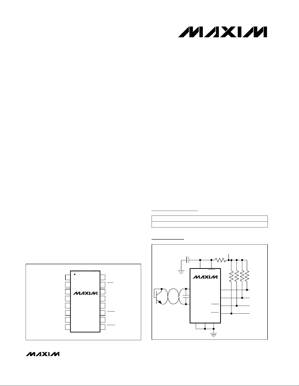
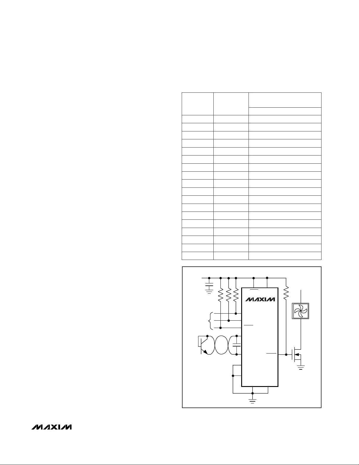
MAX1619
SMBCLK
ADD0 ADD1
V
CC
STBY
GND
ALERT
SMBDATA
DXP
DXN
INTERRUPT
TO µC
FAN
CONTROL
+3V TO +5.5V
200Ω
0.1µF
CLOCK
10k EACH
DATA
2N3904
2200pF
OVERT
___________________Pin Configuration
16
15
14
13
12
11
10
9
1
2
3
4
5
6
7
8
V
CC
N.C.
STBY
SMBCLK
N.C.
SMBDATA
ALERT
ADD0
OVERT
TOP VIEW
MAX1619
QSOP
GND
DXP
ADD1
DXN
N.C.
GND
GND
Typical Operating Circuit
19-1483; Rev 0; 4/99
PART
MAX1619MEE -55°C to +125°C
TEMP. RANGE PIN-PACKAGE
16 QSOP
Ordering Information
SMBus is a registered trademark of Intel Corp.
For free samples & the latest literature: http://www.maxim-ic.com, or phone 1-800-998-8800.
For small orders, phone 1-800-835-8769.
Page 2

MAX1619
Remote/Local Temperature Sensor with DualAlarm Outputs and SMBus Serial Interface
2 _______________________________________________________________________________________
ABSOLUTE MAXIMUM RATINGS
ELECTRICAL CHARACTERISTICS
(VCC= +3.3V, TA= 0°C to +85°C, configuration byte = XCh, unless otherwise noted.)
Stresses beyond those listed under “Absolute Maximum Ratings” may cause permanent damage to the device. These are stress ratings only, and functional
operation of the device at these or any other conditions beyond those indicated in the operational sections of the specifications is not implied. Exposure to
absolute maximum rating conditions for extended periods may affect device reliability.
VCCto GND..............................................................-0.3V to +6V
DXP, ADD_ to GND....................................-0.3V to (V
CC
+ 0.3V)
DXN to GND..........................................................-0.3V to +0.8V
SMBCLK, SMBDATA, ALERT, OVERT,
STBY to GND............................................................-0.3V to +6V
SMBDATA, ALERT, OVERT Current....................-1mA to +50mA
DXN Current .......................................................................±1mA
ESD Protection (all pins, Human Body Model) ..................2000V
Continuous Power Dissipation (T
A
= +70°C)
QSOP (derate 8.30mW/°C above +70°C).....................667mW
Operating Temperature Range .........................-55°C to +125°C
Junction Temperature......................................................+150°C
Storage Temperature Range.............................-65°C to +150°C
Lead Temperature (soldering, 10sec).............................+300°C
T
A
= +60°C to +100°C
Monotonicity guaranteed
ADD0, ADD1; momentary upon power-on reset
DXP forced to 1.5V
Logic inputs
forced to V
CC
or GND
Auto-convert mode
From stop bit to conversion complete (both channels)
VCC, falling edge
TA = 0°C to +85°C
VCCinput, disables A/D conversion, rising edge
Autoconvert mode, average
measured over 4sec. Logic
inputs forced to V
CC
or GND.
CONDITIONS
µA160Address Pin Bias Current
V0.7DXN Source Voltage
µA
81012
80 100 120
Remote-Diode Source Current
%-25 25Conversion Rate Timing Error
ms94 125 156Conversion Time
µA
120 180
35 70
Average Operating Supply Current
-2 2
Bits8Temperature Resolution (Note 1)
µA
5
Standby Supply Current
310
mV50POR Threshold Hysteresis
V1.0 1.7 2.5Power-On Reset Threshold
°C
-3 3
Initial Temperature Error,
Local Diode (Note 2)
V3.0 5.5Supply Voltage Range
V2.60 2.80 2.95Undervoltage Lockout Threshold
mV50Undervoltage Lockout Hysteresis
UNITSMIN TYP MAXPARAMETER
TR = +60°C to +100°C
TR = -55°C to +125°C (Note 4)
-3 3
°C
-5 5
Temperature Error, Remote Diode
(Notes 2, 3)
Including long-term drift
-2.5 2.5
°C
-3.5 3.5
Temperature Error, Local Diode
(Notes 1, 2)
0.25 conv/sec
2.0 conv/sec
TA = +60°C to +100°C
TA = 0°C to +85°C
High level
Low level
ADC AND POWER SUPPLY
SMBus static
Hardware or software standby,
SMBCLK at 10kHz
Page 3
MAX1619
Remote/Local Temperature Sensor with Dual-
Alarm Outputs and SMBus Serial Interface
_______________________________________________________________________________________ 3
ELECTRICAL CHARACTERISTICS (continued)
(VCC= +3.3V, TA= 0°C to +85°C, configuration byte = XCh, unless otherwise noted.)
STBY, SMBCLK, SMBDATA; V
CC
= 3V to 5.5V
t
HIGH
, 90% to 90% points
t
LOW
, 10% to 10% points
(Note 5)
SMBCLK, SMBDATA
Logic inputs forced to VCCor GND
ALERT, OVERT, forced to 5.5V
STBY, SMBCLK, SMBDATA; VCC= 3V to 5.5V
ALERT, OVERT, SMBDATA forced to 0.4V
CONDITIONS
µs4SMBCLK Clock High Time
µs4.7SMBCLK Clock Low Time
kHzDC 100SMBus Clock Frequency
pF5SMBus Input Capacitance
µA-1 1Logic Input Current
µA1
ALERT, OVERT Output High
Leakage Current
V2.2Logic Input High Voltage
V0.8Logic Input Low Voltage
mA6Logic Output Low Sink Current
UNITSMIN TYP MAXPARAMETER
t
SU:DAT
, 10% or 90% of SMBDATA to 10% of SMBCLK
t
SU:STO
, 90% of SMBCLK to 10% of SMBDATA
t
HD:STA
, 10% of SMBDATA to 90% of SMBCLK
t
SU:STA
, 90% to 90% points
ns250
SMBus Data Valid to SMBCLK
Rising-Edge Time
µs4SMBus Stop-Condition Setup Time
µs4SMBus Start-Condition Hold Time
ns500
SMBus Repeated Start-Condition
Setup Time
µs4.7SMBus Start-Condition Setup Time
t
HD:DAT
(Note 6) µs0SMBus Data-Hold Time
Master clocking in data µs1
SMBCLK Falling Edge to SMBus
Data-Valid Time
SMBus INTERFACE
ELECTRICAL CHARACTERISTICS
(VCC= +3.3V, TA= -55°C to +125°C, configuration byte = XCh, unless otherwise noted.) (Note 4)
CONDITIONS
Monotonicity guaranteed
TA= +60°C to +100°C
Bits8Temperature Resolution (Note 1)
-2 2
TR= +60°C to +100°C
TA= -55°C to +125°C
°C
-3 3
Initial Temperature Error,
Local Diode (Note 2)
V3.0 5.5Supply Voltage Range
From stop bit to conversion complete (both channels)
Autoconvert mode
ms94 125 156Conversion Time
%-25 25Conversion Rate Timing Error
-3 3
TR= -55°C to +125°C
°C
UNITSMIN TYP MAX
-5 5
PARAMETER
Temperature Error, Remote Diode
(Notes 2, 3)
ADC AND POWER SUPPLY
Page 4
0
6
3
9
12
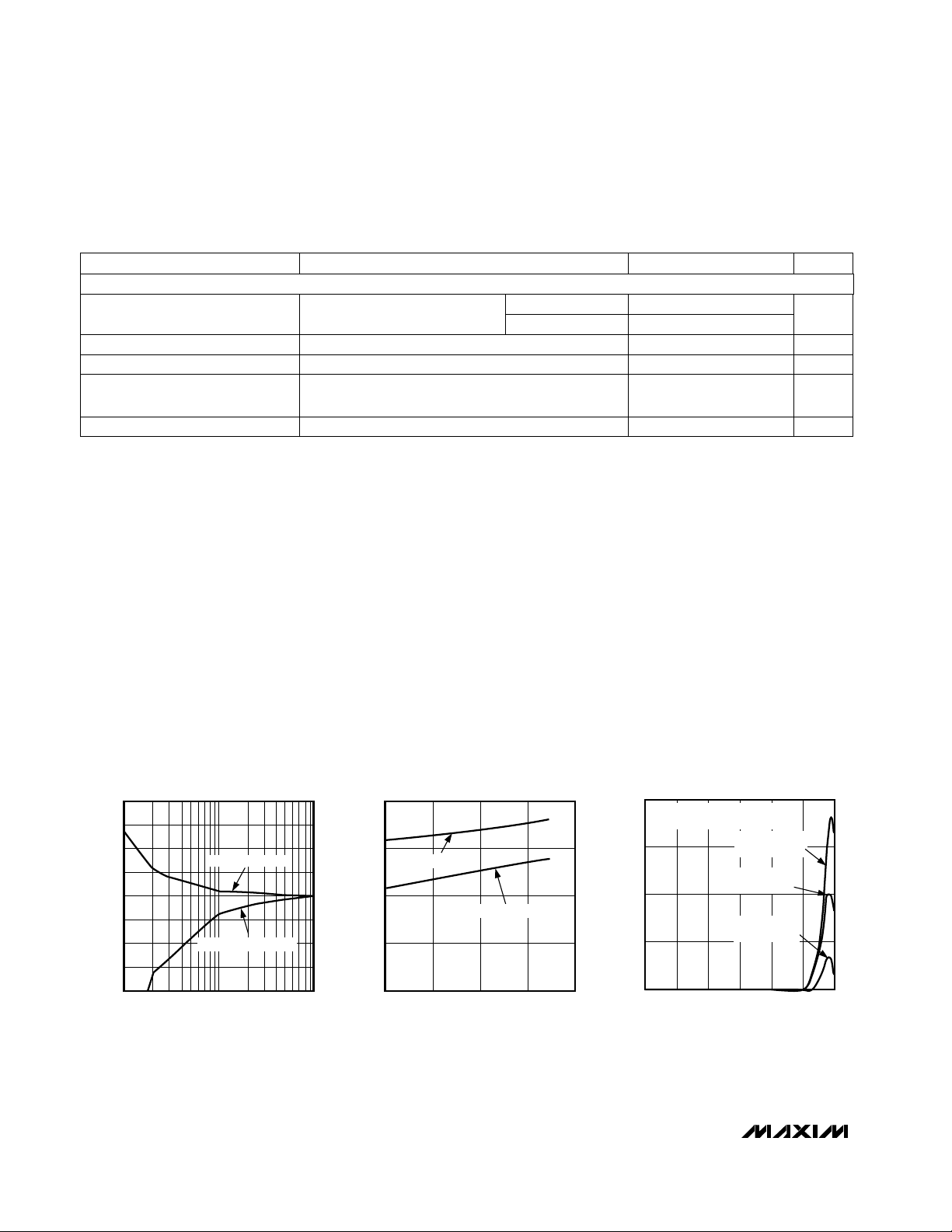
50 5k 500k50k 5M500 50M
TEMPERATURE ERROR vs.
POWER-SUPPLY NOISE FREQUENCY
MAX1619-03
FREQUENCY (Hz)
TEMPERATURE ERROR (°C)
VIN = SQUARE WAVE APPLIED TO
V
CC
WITH NO 0.1µF VCC CAPACITOR
VIN = 250mVp-p
REMOTE DIODE
VIN = 100mVp-p
LOCAL DIODE
VIN = 100mVp-p
REMOTE DIODE
-20
-10
-15
0
-5
10
5
20
15
TEMPERATURE ERROR
vs. PC BOARD RESISTANCE
MAX1619-01
LEAKAGE RESISTANCE (MΩ)
TEMPERATURE ERROR (°C)
1 10 100
PATH = DXP TO GND
PATH = DXP TO VCC (5V)
-2
-1
0
1
2
-50 50 1000 150
TEMPERATURE ERROR
vs. REMOTE-DIODE TEMPERATURE
MAX1619-02
TEMPERATURE (°C)
TEMPERATURE ERROR (°C)
MOTOROLA MMBT3904
ZETEX FMMT3904
RANDOM
SAMPLES
__________________________________________Typical Operating Characteristics
(TA = +25°C, unless otherwise noted.)
MAX1619
Remote/Local Temperature Sensor with DualAlarm Outputs and SMBus Serial Interface
4 _______________________________________________________________________________________
ELECTRICAL CHARACTERISTICS (continued)
(VCC= +3.3V, TA= -55°C to +125°C, configuration byte = XCh, unless otherwise noted.) (Note 4)
Note 1: Guaranteed but not 100% tested.
Note 2: Quantization error is not included in specifications for temperature accuracy. For example, if the MAX1619 device tempera-
ture is exactly +66.7°C, the ADC may report +66°C, +67°C, or +68°C (due to the quantization error plus the +1/2°C offset
used for rounding up) and still be within the guaranteed ±1°C error limits for the +60°C to +100°C temperature range
(Table 2).
Note 3: A remote diode is any diode-connected transistor from Table 1. T
R
is the junction temperature of the remote diode. See
Remote Diode Selection
for remote diode forward voltage requirements.
Note 4: Specifications from -55°C to +125°C are guaranteed by design, not production tested.
Note 5: The SMBus logic block is a static design that works with clock frequencies down to DC. While slow operation is possible, it
violates the 10kHz minimum clock frequency and SMBus specifications, and may monopolize the bus.
Note 6: Note that a transition must internally provide at least a hold time in order to bridge the undefined region (300ns max) of
SMBCLK’s falling edge.
CONDITIONS UNITSMIN TYP MAXPARAMETER
STBY, SMBCLK, SMBDATA
2.2
Logic Input High Voltage V
2.4
STBY, SMBCLK, SMBDATA; VCC= 3V to 5.5V
V0.8Logic Input Low Voltage
ALERT, OVERT forced to 5.5V
µA1
ALERT, OVERT Output High
Leakage Current
Logic inputs forced to VCCor GND µA-2 2Logic Input Current
VCC= 3V
VCC= 5.5V
ALERT, OVERT, SMBDATA forced to 0.4V
mA6Logic Output Low Sink Current
SMBus INTERFACE
Page 5
MAX1619
Remote/Local Temperature Sensor with Dual-
Alarm Outputs and SMBus Serial Interface
_______________________________________________________________________________________
5
0
2
4
8
6
10
TEMPERATURE ERROR vs.
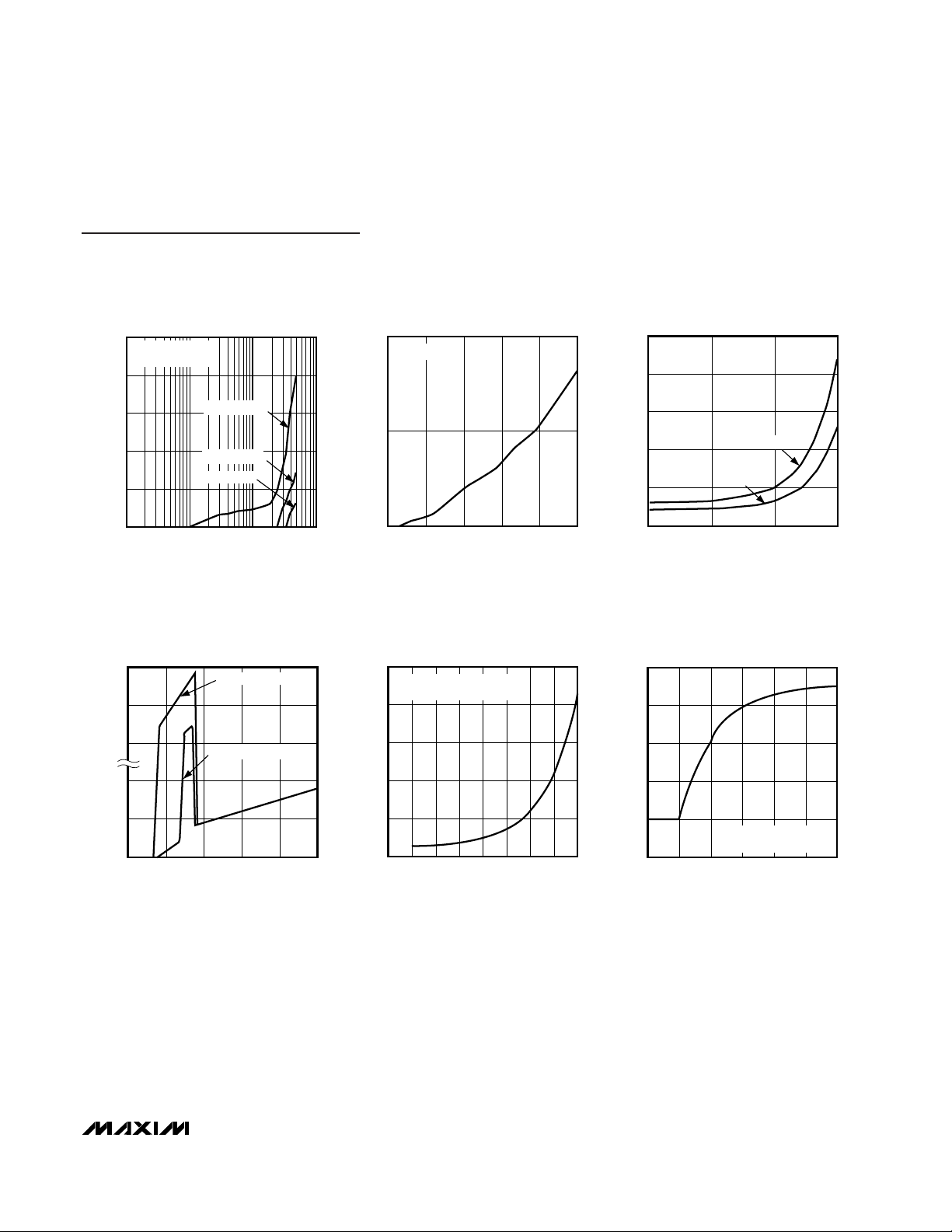
COMMON-MODE NOISE FREQUENCY
MAX1619-04
FREQUENCY (MHz)
TEMPERATURE ERROR (°C)
0.1 10 1001
VIN = 100mVp-p
VIN = SQUARE WAVE
AC-COUPLED TO DXN
VIN = 50mVp-p
VIN = 25mVp-p
0
10
20
04060
80
20 100
TEMPERATURE ERROR vs.
DXP–DXN CAPACITANCE
MAX1619-07
DXP–DXN CAPACITANCE (nF)
TEMPERATURE ERROR (°C)
VCC = 5V
0
100
400
200
300
500
010.0625 40.25 20.125 0.5 8
OPERATING SUPPLY CURRENT
vs. CONVERSION RATE
MAX1619-10
CONVERSION RATE (Hz)
SUPPLY CURRENT (µA)
VCC = 5V
AVERAGED MEASUREMENTS
0
10
20
30
40
50
1 10010 1000
STANDBY SUPPLY CURRENT
vs. CLOCK FREQUENCY
MAX1619-08
SMBCLK FREQUENCY (kHz)
SUPPLY CURRENT (µA)
VCC = 5V
VCC = 3.3V
0
3
60
6
20
100
031425
STANDBY SUPPLY CURRENT
vs. SUPPLY VOLTAGE
MAX1619-09
SUPPLY VOLTAGE (V)
SUPPLY CURRENT (µA)
ADD0, ADD1 = GND
ADD0, ADD1 = HIGH-Z
0
25
100
50
75
125
-2 8 042610
INTERNAL DIODE
RESPONSE TO THERMAL SHOCK
MAX1619-11
TIME (sec)
TEMPERATURE (°C)
16-QSOP IMMERSED
IN +115°C FLUORINERT BATH
Typical Operating Characteristics (continued)
(TA = +25°C, unless otherwise noted.)
Page 6

MAX1619
Remote/Local Temperature Sensor with DualAlarm Outputs and SMBus Serial Interface
6 _______________________________________________________________________________________
Pin Description
Detailed Description
The MAX1619 is a temperature sensor designed to work
in conjunction with an external microcontroller (µC) or
other intelligence in thermostatic, process-control, or
monitoring applications. The µC is typically a powermanagement or keyboard controller, generating SMBus
serial commands either by “bit-banging” general-purpose input/output (GPIO) pins or through a dedicated
SMBus interface block.
Essentially an 8-bit serial analog-to-digital converter
(ADC) with a sophisticated front end, the MAX1619
contains a switched current source, a multiplexer, an
ADC, an SMBus interface, and associated control logic
(Figure 1). Temperature data from the ADC is loaded
into two data registers (local and remote). The remote
temperature data is automatically compared with data
previously stored in four temperature-alarm threshold
registers. One pair of alarm-threshold registers is used
to provide hysteretic fan control; the other pair is used
for alarm interrupt. The local temperature data is available for monitoring.
ADC and Multiplexer
The ADC is an averaging type that integrates over a
60ms period (each channel, typical) with excellent
noise rejection.
The multiplexer automatically steers bias currents
through the remote and local diodes, measures their
forward voltages, and computes their temperatures.
Both channels are automatically converted once the
conversion process has started, either in free-running
or single-shot mode. If one of the two channels is not
used, the device still performs both measurements, and
the user can simply ignore the results of the unused
channel.
The DXN input is biased at 0.65V above ground by an
internal diode to set up the analog-to-digital (A/D)
inputs for a differential measurement. The worst-case
DXP–DXN differential input voltage range is 0.25V to
0.95V.
Excess resistance in series with the remote diode caus-
es about +1/2°C error per ohm. Likewise, 200µV of offset voltage forced on DXP–DXN causes about 1°C error.
SMBus Serial-Data Input/Output, Open DrainSMBDATA12
SMBus Serial-Clock InputSMBCLK14
Hardware Standby Input. Temperature and comparison threshold data are retained in standby mode.
Low = standby mode, high = operate mode.
STBY
15
SMBus Address Select Pin (Table 8). ADD0 and ADD1 are sampled upon power-up. Excess capacitance
(>50pF) at the address pins when floating may cause address-recognition problems.
ADD16
GroundGND7, 8
SMBus Slave Address Select PinADD010
SMBus Alert (interrupt) Output, Open Drain
ALERT
11
Combined Current Sink and A/D Negative Input. DXN is normally internally biased to a diode voltage
above ground.
DXN4
Combined Current Source and A/D Positive Input for Remote-Diode Channel. Do not leave DXP floating;
connect DXP to DXN if no remote diode is used. Place a 2200pF capacitor between DXP and DXN for
noise filtering.
DXP3
PIN
Supply Voltage Input, 3V to 5.5V. Bypass to GND with a 0.1µF capacitor. A 200Ω series resistor is recommended but not required for additional noise filtering.
V
CC
1
FUNCTIONNAME
Overtemperature Alarm Output, Open Drain. This is an unlatched alarm output that responds only to the
remote diode temperature.
OVERT
9
Not internally connected. Connect to GND to act against leakage paths from VCCto DXP.GND2
No Connection. Not internally connected. May be used for PC board trace routing.N.C.
5, 13,
16
Page 7

MAX1619
Remote/Local Temperature Sensor with Dual-
Alarm Outputs and SMBus Serial Interface
_______________________________________________________________________________________ 7
Figure 1. Functional Diagram
REMOTE
MUX
LOCAL
REMOTE TEMPERATURE
DATA REGISTER
HIGH-TEMPERATURE THRESHOLD
(REMOTE T
HIGH
)
LOW-TEMPERATURE THRESHOLD
(REMOTE T
LOW
)
DIGITAL COMPARATOR
(REMOTE)
LOCAL TEMPERATURE
DATA REGISTER
HIGH-TEMPERATURE THRESHOLD
(REMOTE T
MAX
)
HYSTERESIS THRESHOLD
(REMOTE T
HYST
)
DIGITAL COMPARATOR
(REMOTE OVERTEMP)
COMMAND BYTE
(INDEX) REGISTER
SMBDATA
SMBCLK
ADDRESS
DECODER
READ WRITE
CONTROL
LOGIC
SMBus
ADD1ADD0STBY
STATUS BYTE REGISTER
CONFIGURATION
BYTE REGISTER
CONVERSION RATE
REGISTER
ALERT RESPONSE
ADDRESS REGISTER
SELECTED VIA
SLAVE ADD = 0001 100
ADC
+
DIODE
FAULT
DXP
DXN
GND
V
CC
-
+
-
+
-
8
8
8
8
8
88
2
7
ALERT
OVERT
QS
R
Q
S
R
POL
MAX1619
Page 8

A/D Conversion Sequence
If a Start command is written (or generated automatically in the free-running auto-convert mode), both channels
are converted, and the results of both measurements
are available after the end of conversion. A BUSY status
bit in the status byte shows that the device is actually
performing a new conversion; however, even if the ADC
is busy, the results of the previous conversion are
always available.
Remote-Diode Selection
Temperature accuracy depends on having a good-quality, diode-connected small-signal transistor. Accuracy
has been experimentally verified for all the devices listed in Table 1. The MAX1619 can also directly measure
the die temperature of CPUs and other integrated circuits having on-board temperature-sensing diodes.
The transistor must be a small-signal type with a relatively high forward voltage; otherwise, the A/D input
voltage range can be violated. The forward voltage
must be greater than 0.25V at 10µA; check to ensure
this is true at the highest expected temperature. The
forward voltage must be less than 0.95V at 100µA;
check to ensure this is true at the lowest expected
temperature. Large power transistors don’t work. Also,
ensure that the base resistance is less than 100Ω. Tight
specifications for forward-current gain (+50 to +150, for
example) indicate that the manufacturer has good
process controls and that the devices have consistent
VBEcharacteristics.
For heatsink mounting, the 500-32BT02-000 thermal
sensor from Fenwal Electronics is a good choice. This
device consists of a diode-connected transistor, an
aluminum plate with screw hole, and twisted-pair cable
(Fenwal Inc., Milford, MA, 508-478-6000).
Thermal Mass and Self-Heating
Thermal mass can seriously degrade the MAX1619’s
effective accuracy. The thermal time constant of the
QSOP-16 package is about 4sec in still air. To settle to
within +1°C after a sudden +100°C change, the
MAX1619 junction temperature requires about five time
constants. The use of smaller packages for remote sensors, such as SOT23s, improves the situation. Take
care to account for thermal gradients between the heat
source and the sensor, and ensure that stray air currents across the sensor package do not interfere with
measurement accuracy.
Self-heating does not significantly affect measurement
accuracy. Remote-sensor self-heating due to the diode
current source is negligible. For the local diode, the
worst-case error occurs when auto-converting at the
fastest rate and simultaneously sinking maximum current at the ALERT and OVERT outputs. For example, at
an 8Hz rate and with ALERT and OVERT each sinking
1mA, the typical power dissipation is:
(V
CC
)(450µA) + 2(0.4V)(1mA)
Package θJAis about 120°C/W, so with VCC= 5V and
no copper PC board heatsinking, the resulting temperature rise is:
∆T = 3.1mW(120°C/W) = 0.36°C
Even with these contrived circumstances, it is difficult
to introduce significant self-heating errors.
ADC Noise Filtering
The ADC is an integrating type with inherently good
noise rejection, especially of low-frequency signals such
as 60Hz/120Hz power-supply hum. Micropower operation places constraints on high-frequency noise rejection;
therefore, careful PC board layout and proper external
noise filtering are required for high-accuracy remote
measurements in electrically noisy environments.
High-frequency EMI is best filtered at DXP and DXN
with an external 2200pF capacitor. This value can be
increased to about 3300pF (max), including cable
capacitance. Capacitance higher than 3300pF introduces errors due to the rise time of the switched current source.
Nearly all noise sources tested cause the ADC measurements to be higher than the actual temperature, typically
by +1°C to +10°C, depending on the frequency and
amplitude (see
Typical Operating Characteristics
).
MAX1619
Remote/Local Temperature Sensor with DualAlarm Outputs and SMBus Serial Interface
8 _______________________________________________________________________________________
CMPT3904Central Semiconductor (USA)
MMBT3904Fairchild Semiconductor (USA)
SST3904Rohm Semiconductor (Japan)
FMMT3904CT-NDZetex (England)
MANUFACTURER MODEL NUMBER
SMBT3904Siemens (Germany)
Table 1. Remote-Sensor Transistor
Manufacturers
Note: Transistors must be diode-connected (base shorted to
collector).
MMBT3904Motorola (USA)
Page 9

PC Board Layout
1) Place the MAX1619 as close as practical to the
remote diode. In a noisy environment, such as a
computer motherboard, this distance can be 4 inches to 8 inches (typical) or more as long as the worst
noise sources (such as CRTs, clock generators,
memory buses, and ISA/PCI buses) are avoided.
2) Do not route the DXP–DXN lines next to the deflection coils of a CRT. Also, do not route the traces
across a fast memory bus, which can easily introduce +30°C error, even with good filtering.
Otherwise, most noise sources are fairly benign.
3) Route the DXP and DXN traces in parallel and in
close proximity to each other, away from any highvoltage traces such as +12VDC. Leakage currents
from PC board contamination must be dealt with
carefully, since a 10MΩ leakage path from DXP to
ground causes about +1°C error.
4) Connect guard traces to GND on either side of the
DXP–DXN traces (Figure 2). With guard traces in
place, routing near high-voltage traces is no longer
an issue.
5) Route through as few vias and crossunders as possible to minimize copper/solder thermocouple effects.
6) When introducing a thermocouple, make sure that
both the DXP and the DXN paths have matching
thermocouples. In general, PC board-induced thermocouples are not a serious problem. A copper-solder thermocouple exhibits 3µV/°C, and it takes
about 200µV of voltage error at DXP–DXN to cause
a +1°C measurement error. So, most parasitic thermocouple errors are swamped out.
7) Use wide traces. Narrow ones are more inductive
and tend to pick up radiated noise. The 10 mil
widths and spacings recommended in Figure 2
aren’t absolutely necessary (as they offer only a
minor improvement in leakage and noise), but try to
use them where practical.
8) Keep in mind that copper can’t be used as an EMI
shield, and only ferrous materials, such as steel, work
well. Placing a copper ground plane between the
DXP-DXN traces and traces carrying high-frequency
noise signals does not help reduce EMI.
PC Board Layout Checklist
• Place the MAX1619 close to a remote diode.
• Keep traces away from high voltages (+12V bus).
• Keep traces away from fast data buses and CRTs.
• Use recommended trace widths and spacings.
• Place a ground plane under the traces.
• Use guard traces flanking DXP and DXN and connecting to GND.
• Place the noise filter and the 0.1 µF V
CC
bypass
capacitors close to the MAX1619.
• Add a 200Ω resistor in series with VCCfor best noise
filtering (see
Typical Operating Circuit
).
Twisted Pair and Shielded Cables
For remote-sensor distances longer than 8 inches, or in
particularly noisy environments, a twisted pair is recommended. Its practical length is 6 feet to 12 feet (typical)
before noise becomes a problem, as tested in a noisy
electronics laboratory. For longer distances, the best
solution is a shielded twisted pair like that used for audio
microphones. For example, the Belden 8451 works well
in a noisy environment for distances up to 100 feet.
Connect the twisted pair to DXP and DXN and the shield
to GND, and leave the shield’s remote end unterminated.
Excess capacitance at DX_ limits practical remote sensor distances (see
Typical Operating Characteristics
).
For very long cable runs, the cable’s parasitic capacitance often provides noise filtering, so the 2200pF
capacitor can often be removed or reduced in value.
Cable resistance also affects remote-sensor accuracy;
1Ω series resistance introduces about +1/2°C error.
Low-Power Standby Mode
Standby mode disables the ADC and reduces the supply-current drain to 3µA (typical). Enter standby mode
by forcing the STBY pin low or via the RUN/STOP bit in
the configuration byte register. Hardware and software
standby modes behave almost identically: all data is
retained in memory, and the SMB interface is alive and
listening for reads and writes. The only difference is
that in hardware standby mode, the one-shot command
does not initiate a conversion.
Standby mode is not a shutdown mode. With activity on
the SMBus, extra supply current is drawn (see
Typical
Operating Characteristics
). In software standby mode,
MAX1619
Remote/Local Temperature Sensor with Dual-
Alarm Outputs and SMBus Serial Interface
_______________________________________________________________________________________ 9
MINIMUM
10 MILS
10 MILS
10 MILS
10 MILS
GND
DXN
DXP
GND
Figure 2. Recommended DXP/DXN PC Traces
Page 10

the MAX1619 can be forced to perform A/D conversions
via the one-shot command, despite the RUN/STOP bit
being high.
Activate hardware standby mode by forcing the STBY
pin low. In a notebook computer, this line may be connected to the system SUSTAT# suspend-state signal.
The STBY pin low state overrides any software conversion
command. If a hardware or software standby command
is received while a conversion is in progress, the conversion cycle is truncated, and the data from that conversion
is not latched into either temperature reading register.
The previous data is not changed and remains available.
The OVERT output continues to function in both hardware and software standby modes. If the overtemp limits are adjusted while in standby mode, the digital
comparator checks the new values and puts the OVERT
pin in the correct state based on the last valid ADC conversion. The last valid ADC conversion may include a
conversion performed using the one-shot command.
Supply-current drain during the 125ms conversion period is always about 450µA. Slowing down the conversion
rate reduces the average supply current (see
Typical
Operating Characteristics
). Between conversions, the
instantaneous supply current is about 25µA due to the
current consumed by the conversion rate timer. In
standby mode, supply current drops to about 3µA. At
very low supply voltages (under the power-on-reset
threshold), the supply current is higher due to the
address pin bias currents. It can be as high as 100µA,
depending on ADD0 and ADD1 settings.
SMBus Digital Interface
From a software perspective, the MAX1619 appears as a
set of byte-wide registers that contain temperature data,
alarm threshold values, or control bits. A standard
SMBus 2-wire serial interface is used to read temperature data and write control bits and alarm threshold data.
Each A/D channel within the device responds to the
same SMBus slave address for normal reads and writes.
The MAX1619 employs four standard SMBus protocols:
Write Byte, Read Byte, Send Byte, and Receive Byte
(Figure 3). The shorter Receive Byte protocol allows
quicker transfers, provided that the correct data register
was previously selected by a Read Byte instruction. Use
caution with the shorter protocols in multi-master sys-
MAX1619
Remote/Local Temperature Sensor with DualAlarm Outputs and SMBus Serial Interface
10 ______________________________________________________________________________________
ACK
7 bits
ADDRESS ACKWR
8 bits
DATA ACK
1
P
8 bits
S COMMAND
Write Byte Format
Read Byte Format
Send Byte Format Receive Byte Format
Slave Address:
equivalent to chip-select
line of a 3-wire interface
Command Byte: selects
which register you are
writing to
Data Byte: data goes into the register
set by the command byte (to set
thresholds, configuration masks, and
sampling rate)
ACK
7 bits
ADDRESS ACKWR S ACK
8 bits
DATA
7 bits
ADDRESS RD
8 bits
/// PS COMMAND
Slave Address:
equivalent to
chip-select line
Command Byte: selects
which register you are
reading from
Slave Address: repeated
due to change in dataflow direction
Data Byte: reads from
the register set by the
command byte
ACK
7 bits
ADDRESS WR
8 bits
COMMAND ACK PS ACK
7 bits
ADDRESS RD
8 bits
DATA /// PS
Command Byte: sends command with no data; usually
used for one-shot command
Data Byte: reads data from
the register commanded
by the last Read Byte or
Write Byte transmission;
also used for SMBus Alert
Response return address
S = Start condition Shaded = Slave transmission
P = Stop condition /// = Not acknowledged
Figure 3. SMBus Protocols
Page 11
tems, since a second master could overwrite the command byte without informing the first master.
The temperature data format is 7 bits plus sign in two’s
complement form for each channel, with each data bit representing 1°C (Table 2), transmitted MSB first. Measurements are offset by +1/2°C to minimize internal rounding
errors; for example, +99.6°C is reported as +100°C.
Alarm Threshold Registers
Two registers store ALERT threshold limits, with hightemperature (T
HIGH
) and low-temperature (T
LOW
) registers for the remote A/D channel. There are no
comparison registers for the local A/D channel. If either
measured temperature
equals or exceeds
the corresponding alarm threshold value, an ALERT interrupt is
asserted. The power-on-reset (POR) state of the T
HIGH
register is full scale (0111 1111, or +127°C). The POR
state of the T
LOW
register is 1100 1001 or -55°C.
Two additional alarm threshold registers control the
OVERT output (see OVERT
Alarm Output
section), T
MAX
and T
HYST
. The POR state of T
MAX
is +100°C, and
T
HYST
is +95°C.
OOVVEERRTT
Alarm Output for Fan Control
The OVERT output is an unlatched open-drain output that
behaves as a thermostat to control a fan (Figure 4). When
using the SMBus interface, the polarity of the OVERT pin
(active-low at POR) can be inverted via bit 5 in the configuration byte. OVERT’s current state can be read in the
status byte.
OVERT can also be used to control a fan without system
intervention. OVERT goes low when the remote temperature rises above T
MAX
and won’t go high again until the
temperature drops below T
HYST
. The power-up default
settings for T
MAX
and T
HYST
(+100°C and +95°C,
respectively) allow the MAX1619 to be used in standalone thermostat applications where connection to an
SMBus serial bus isn’t required.
Diode Fault Alarm
There is a continuity fault detector at DXP that detects
whether the remote diode has an open-circuit condition. At the beginning of each conversion, the diode
fault is checked, and the status byte is updated. This
fault detector is a simple voltage detector; if DXP rises
above VCC- 1V (typical) due to the diode current
source, a fault is detected. Note that the diode fault
isn’t checked until a conversion is initiated, so immediately after power-on reset the status byte indicates no
fault is present, even if the diode path is broken.
MAX1619
Remote/Local Temperature Sensor with Dual-
Alarm Outputs and SMBus Serial Interface
______________________________________________________________________________________ 11
DIGITAL OUTPUT
DATA BITS
0 111 1111+127+127.00
0 111 1111
0 111 1110+126+126.00
+127+126.50
0 001 1001
0 000 0001+1+0.50
0 000 0000
0 000 000000.00
ROUNDED
TEMP.
(°C)
TEMP.
(°C)
0+0.25
+25+25.25
0 000 0000
0 000 00000-0.50
1 111 1111
1 111 1111-1-1.00
-1-0.75
1 110 0111
1 110 0111-25-25.50
1 100 1001
1 100 1001-55-55.00
0-0.25
-55-54.75
-25-25.00
1 011 1111
1 011 1111-65-70.00
-65-65.00
Table 2. Data Format (Two’s Complement)
SIGN MSB LSB
0 111 1111+127+130.00
Figure 4. Fan Control Application
+3V TO +5.5V
SMBUS
SERIAL
INTERFACE
(TO HOST)
2N3904
STBY V
MAX1619
SMBCLK
SMBDATA
ALERT
DXP
DXN
ADD0
ADD1
GND
CC
OVERT
PGND
+12V
Page 12

If the remote channel is shorted (DXP to DXN or DXP to
GND), the ADC reads 0000 0000 so as not to trip either
the T
HIGH
or T
LOW
alarms at their POR settings. In
applications that are never subjected to 0°C in normal
operation, a 0000 0000 result can be checked to indicate a fault condition in which DXP is accidentally short
circuited. Similarly, if DXP is short circuited to VCC, the
ADC reads +127°C for both remote and local channels,
and the ALERT and OVERT outputs are activated.
AALLEERRTT
Interrupts
The ALERT interrupt output signal is latched and can
only be cleared by reading the Alert Response address.
Interrupts are generated in response to T
HIGH
and T
LOW
comparisons and when the remote diode is disconnected (for continuity fault detection). The interrupt does not
halt automatic conversions; new temperature data continues to be available over the SMBus interface after
ALERT is asserted. The interrupt output pin is open-drain
so that devices can share a common interrupt line. The
interrupt rate can never exceed the conversion rate.
The interface responds to the SMBus Alert Response
address, an interrupt pointer return-address feature
(see
Alert Response Address
section). Prior to taking
corrective action, always check to ensure that an interrupt is valid by reading the current temperature.
To prevent reoccurring interrupts, the MAX1619 asserts
ALERT only once per crossing of a given temperature
threshold. To enable a new interrupt, the value in the
limit register that triggered the interrupt must be rewritten. Note that other interrupt conditions can be caused
by crossing the opposite temperature threshold, or a
diode fault can still cause an interrupt.
Example: the remote temperature reading crosses
T
HIGH
, activating ALERT. The host responds to the
interrupt and reads the Alert Response address, clearing the interrupt. The system may also read the status
byte at this time. The condition that caused the interrupt
persists, but no new ALERT interrupt is issued. Finally,
the host writes a new value to T
HIGH
. This enables the
device to generate a new T
HIGH
interrupt if the alert
condition still exists.
Alert Response Address
The SMBus Alert Response interrupt pointer provides
quick fault identification for simple slave devices that lack
the complex, expensive logic needed to be a bus master.
Upon receiving an ALERT interrupt signal, the host master can broadcast a Receive Byte transmission to the
Alert Response slave address (0001 100). Then any slave
device that generated an interrupt attempts to identify
itself by putting its own address on the bus (Table 3).
The Alert Response can activate several different slave
devices simultaneously, similar to the I2C™ General
Call. If more than one slave attempts to respond, bus
arbitration rules apply, and the device with the lower
address code wins. The losing device does not generate an acknowledge and continues to hold the ALERT
line low until serviced (implies that the host interrupt
input is level-sensitive). Successful reading of the alert
response address clears the interrupt latch.
Command Byte Functions
The 8-bit command byte register (Table 4) is the master
index that points to the other registers within the
MAX1619. The register’s POR state is 0000 0001 so
that a Receive Byte transmission (a protocol that lacks
the command byte) that occurs immediately after POR
returns the current remote temperature data.
The one-shot command immediately forces a new conversion cycle to begin. In software standby mode
(RUN/STOP bit = high), a new conversion is begun, after
which the device returns to standby mode. If a conversion
is in progress when a one-shot command is received, the
command is ignored. If a one-shot command is received
in auto-convert mode (RUN/STOP bit = low) between conversions, a new conversion begins, the conversion rate
timer is reset, and the next automatic conversion takes
place after a full delay elapses.
Configuration Byte Functions
The configuration byte register (Table 5) is used to
mask (disable) interrupts, to put the device in software
standby mode, to change the polarity of the OVERT
output, and to enable the write-once protection. The
lowest two bits are internally set to zeros, making them
“don’t care” bits. This register’s contents can be read
back over the serial interface.
MAX1619
Remote/Local Temperature Sensor with DualAlarm Outputs and SMBus Serial Interface
12 ______________________________________________________________________________________
I2C is a trademark of Philips Corp.
Table 3. Read Format for Alert Response
Address (0001100)
ADD66
Provide the current MAX1619
slave address
FUNCTION
ADD55
ADD44
ADD33
ADD22
ADD11
ADD7
7
(MSB)
1
0
(LSB)
Logic 1
BIT NAME
Page 13

MAX1619
Remote/Local Temperature Sensor with Dual-
Alarm Outputs and SMBus Serial Interface
______________________________________________________________________________________ 13
Table 4. Command-Byte Bit Assignments
*
If the device is in hardware standby mode at POR, both temperature registers read 0°C.
Read remote temperature: returns latest temperatureRRTE 01h
00h
COMMAND
0000 0000*
0000 0000*
POR STATE
Read configuration byteRCL 03h
02h
0000 1100
N/A Read status byte (flags, busy signal)RSL
Read remote T
MAX
limitRRTM 10h
Read local temperature: returns latest temperatureRLTS
04h
01100100
0000 0010
Read remote T
HIGH
limitRRHI 07h
11h
0111 1111
01011111 Read remote T
HYST
limitRRTH
Read conversion rate byte
REGISTER
RCRA
Write configuration byteWCA 09h
08h
N/A
1100 1001
FUNCTION
Write remote T
MAX
limitWRTM 12h
0Ah
N/A
N/A Write conversion rate byteWCRW
Write remote T
HIGH
limitWRHA 0Dh
Read remote T
LOW
limitRRLS
13h
N/A
N/A
One-shot command OSHT 0Fh
0Eh
N/A
N/A Write remote T
LOW
limitWRLN
Write remote T
HYST
limitWRTH
RUN/
STOP
6 0
0
POR STATE
Standby mode control bit. If high, the device immediately stops converting and
enters standby mode. If low, the device converts in either one-shot or timer
mode.
Masks all ALERT interrupts when high.
FUNCTION
POL5 0
Determines the polarity of the OVERT output:
0 = active low (low when overtemp)
1 = active high
MASK7 (MSB)
BIT NAME
Table 5. Configuration-Byte Bit Assignments
Write addressWADD FDh
FCh
N/A
N/A
Read device ID codeDEV ID FFh
FEh
0000 0100
0100 1101 Read manufacturer ID codeMFG ID
Write software PORSPOR
PROT4 0
When asserted high, locks out all subsequent writes to:
[] Configuration register bits 6, 5, 4, 3, 2 (RUN/STOP, POL, PROT, ID1, ID2)
[] T
MAX
register
[] T
HYST
register
[] Conversion rate register
[] Diode Current
ID13 1 Reduces the diode current by 5µA when set low.
ID22 1 Reduces the diode current by 2.5µA when set low.
RFU1–0 0 Reserved for future use.
Page 14
MAX1619
Remote/Local Temperature Sensor with DualAlarm Outputs and SMBus Serial Interface
14 ______________________________________________________________________________________
Write-Once Protection
Write-once protection allows the host BIOS code to
configure the MAX1619 in a particular way, and then
protect that configuration against data corruption in the
host that might cause spurious writes to the MAX1619.
In particular, write protection allows a foolproof overtemperature override that forces the fan on 100% via
OVERT independent of the host system. The write-protection bit (bit 4), once set high, can’t be reset to low
except by a hardware power-on reset. A SPOR (software POR) will not reset this bit.
Status Byte Functions
The status byte register (Table 6) indicates which (if
any) temperature thresholds have been exceeded. This
byte also indicates whether or not the ADC is converting
and whether there is an open circuit in the remote diode
DXP–DXN path. The status byte is cleared by any successful read of the status byte, unless the fault persists.
The status of bit1 (OVER) follows the state of OVERT
exactly. Note that the ALERT interrupt latch is not automatically cleared when the status flag bit is cleared.
When autoconverting, if the T
HIGH
and T
LOW
limits are
close together, it’s possible for both high-temp and lowtemp status bits to be set, depending on the amount of
time between status read operations (especially when
converting at the fastest rate). In these circumstances, it’s
best not to rely on the status bits to indicate reversals in
long-term temperature changes. Instead, use a current
temperature reading to establish the trend direction.
Conversion Rate Byte
The conversion rate register (Table 7) programs the time
interval between conversions in free-running autoconvert
mode. This variable rate control reduces the supply current in portable-equipment applications. The conversion
rate byte’s POR state is 02h (0.25Hz). The MAX1619
looks only at the 3 LSB bits of this register, so the upper 5
bits are “don’t care” bits, which should be set to zero. The
conversion rate tolerance is ±25% at any rate setting.
Valid A/D conversion results for both channels are available one total conversion period (125ms nominal, 156ms
maximum) after initiating a conversion, whether conversion is initiated via the RUN/STOP bit, hardware STBY
pin, one-shot command, or initial power-up. Changing the
conversion rate can also affect the delay until new results
are available (Table 8).
Manufacturer and Device ID Codes
Two ROM registers provide manufacturer and device ID
codes (Table 4). Reading the manufacturer ID returns
4Dh, which is the ASCII code “M” (for Maxim). Reading
the device ID returns 04h, indicating a MAX1619 device.
If READ WORD 16-bit SMBus protocol is employed
(rather than the 8-bit READ BYTE), the least significant
byte contains the data and the most significant byte contains 00h in both cases.
Slave Addresses
The MAX1619 appears to the SMBus as one device
having a common address for both ADC channels. The
device address can initially be set to one of nine different values by pin-strapping ADD0 and ADD1 so that
more than one MAX1619 can reside on the same bus
without address conflicts (Table 9).
Table 6. Status-Byte Bit Assignments
*
The HIGH and LOW temperature alarm flags stay high until
cleared by POR or until status register is read.
RFU6 Reserved for future use.
A high indicates that the ADC is busy
converting.
FUNCTION
RFU5 Reserved for future use.
RHIGH*4
A high indicates that the remote hightemperature alarm has activated.
RLOW*3
A high indicates that the remote lowtemperature alarm has activated.
OPEN*2
A high indicates a remote-diode continuity (open-circuit) fault.
OVER1
BUSY
7
(MSB)
This bit follows the state of the OVERT
pin exactly, in real time (unlatched).
RFU
0
(LSB)
Reserved for future use.
BIT NAME
Table 7. Conversion-Frequency Control
Byte
0.12501h 33
30
AVERAGE SUPPLY
CURRENT
(µA typ, at VCC= 3.3V)
0.2502h 35
0.503h 48
104h 70
205h 128
406h
0.062500h
225
807h 425
RFU
08h to
FFh
—
DATA
CONVERSION
FREQUENCY
(Hz)
Page 15

The address pin states are checked at POR and SPOR
only, and the address data stays latched to reduce quiescent supply current due to the bias current needed
for high-Z state detection. A new device address can be
written using the Write Address Command FDh.
The MAX1619 also responds to the SMBus Alert Response
slave address (see the
Alert Response Address
section).
POR and UVLO
The MAX1619 has a volatile memory. To prevent ambiguous power-supply conditions from corrupting the data in
memory and causing erratic behavior, a POR voltage
detector monitors VCCand clears the memory if VCCfalls
below 1.7V (typical, see
Electrical Characteristics
table).
When power is first applied and VCCrises above 1.75V
(typical), the logic blocks begin operating, although reads
and writes at VCClevels below 3V are not recommended.
A second VCCcomparator, the ADC UVLO comparator,
prevents the ADC from converting until there is sufficient
headroom (VCC= 2.8V typical).
The SPOR software POR command can force a power-on
reset of the MAX1619 registers via the serial interface. Use
the SEND BYTE protocol with COMMAND = FCh. This is
most commonly used to reconfigure the slave address of
the MAX1619 “on the fly,” where external hardware has
forced new states at the ADD0 and ADD1 address pins
prior to the software POR. The new address takes effect
less than 100µs after the SPOR transmission stop condition.
Power-Up Defaults:
• Interrupt latch is cleared.
• Address select pins are sampled.
• ADC begins auto-converting at a 0.25Hz rate.
• Command byte is set to 01h to facilitate quick
remote Receive Byte queries.
• T
HIGH
and T
LOW
registers are set to +127°C and
-55°C, respectively.
• T
MAX
and T
HYST
are set to +100°C and +95°C,
respectively.
• OVERT polarity is active low.
MAX1619
Remote/Local Temperature Sensor with Dual-
Alarm Outputs and SMBus Serial Interface
______________________________________________________________________________________ 15
Table 8. RLTS and RRTE Temperature Register Update Timing Chart
n/a (0.25Hz)
NEW CONVERSION
FREQUENCY (CHANGED VIA
WRITE TO WCRW)
Power-on resetAutoconvert
OPERATING MODE CONVERSION INITIATED BY:
156ms max
TIME UNTIL RLTS AND RRTE
ARE UPDATED
156ms maxn/a
One-shot command, while idling
between automatic conversions
Autoconvert
When current conversion is
complete (1-shot is ignored)
20sec
n/a
0.0625HzRate timerAutoconvert
One-shot command that occurs
during a conversion
Autoconvert
10sec
5sec
0.125Hz
0.25HzRate timerAutoconvert
2.5sec
1.25sec
0.5Hz
1HzRate timerAutoconvert
Rate timerAutoconvert
Rate timerAutoconvert
625ms
312.5ms
2Hz
4HzRate timerAutoconvert
237.5ms
156ms
8Hz
n/a
STBY pin
Hardware Standby
Rate timerAutoconvert
Rate timerAutoconvert
156ms
156ms
n/a
n/aOne-shot commandSoftware Standby
RUN/STOP bitSoftware Standby
Table 9. POR Slave Address Decoding
(ADD0 and ADD1)
Note: High-Z means that the pin is left unconnected and floating.
0011 001High-ZGND
0011 000
ADDRESS
0101 001GNDHigh-Z
0011 010V
CC
GND
0101 011V
CC
High-Z
0101 010
1001 101High-ZV
CC
1001 100
GNDGND
GNDV
CC
High-ZHigh-Z
1001 110V
CC
V
CC
ADD0 ADD1
Page 16

MAX1619
Remote/Local Temperature Sensor with DualAlarm Outputs and SMBus Serial Interface
16 ______________________________________________________________________________________
Figure 6. SMBus Read Timing Diagram
Figure 5. SMBus Write Timing Diagram
SMBCLK
A = START CONDITION
B = MSB OF ADDRESS CLOCKED INTO SLAVE
C = LSB OF ADDRESS CLOCKED INTO SLAVE
D = R/W BIT CLOCKED INTO SLAVE
AB CDEFG H
I
J
SMBDATA
t
SU:STAtHD:STA
t
LOW
t
HIGH
t
SU:DAT
t
SU:STO
t
BUF
K
E = SLAVE PULLS SMBDATA LINE LOW
F = ACKNOWLEDGE BIT CLOCKED INTO MASTER
G = MSB OF DATA CLOCKED INTO MASTER
H = LSB OF DATA CLOCKED INTO MASTER
I = ACKNOWLEDGE CLOCK PULSE
J = STOP CONDITION
K = NEW START CONDITION
SMBCLK
SMBDATA
A = START CONDITION
B = MSB OF ADDRESS CLOCKED INTO SLAVE
C = LSB OF ADDRESS CLOCKED INTO SLAVE
D = R/W BIT CLOCKED INTO SLAVE
E = SLAVE PULLS SMBDATA LINE LOW
AB CDEFG HIJ
t
LOWtHIGH
t
SU:STA
t
HD:STA
t
SU:DAT
F = ACKNOWLEDGE BIT CLOCKED INTO MASTER
G = MSB OF DATA CLOCKED INTO SLAVE
H = LSB OF DATA CLOCKED INTO SLAVE
I = SLAVE PULLS SMBDATA LINE LOW
t
HD:DAT
K
t
SU:STO
J = ACKNOWLEDGE CLOCKED INTO MASTER
K = ACKNOWLEDGE CLOCK PULSE
L = STOP CONDITION, DATA EXECUTED BY SLAVE
M = NEW START CONDITION
M
L
t
BUF
Page 17

MAX1619
Remote/Local Temperature Sensor with Dual-
Alarm Outputs and SMBus Serial Interface
______________________________________________________________________________________ 17
Listing 1. Pseudocode Example
Page 18
MAX1619
Remote/Local Temperature Sensor with DualAlarm Outputs and SMBus Serial Interface
18 ______________________________________________________________________________________
Listing 1. Pseudocode Example (continued)
Page 19

MAX1619
Remote/Local Temperature Sensor with Dual-
Alarm Outputs and SMBus Serial Interface
______________________________________________________________________________________ 19
Listing 1. Pseudocode Example (continued)
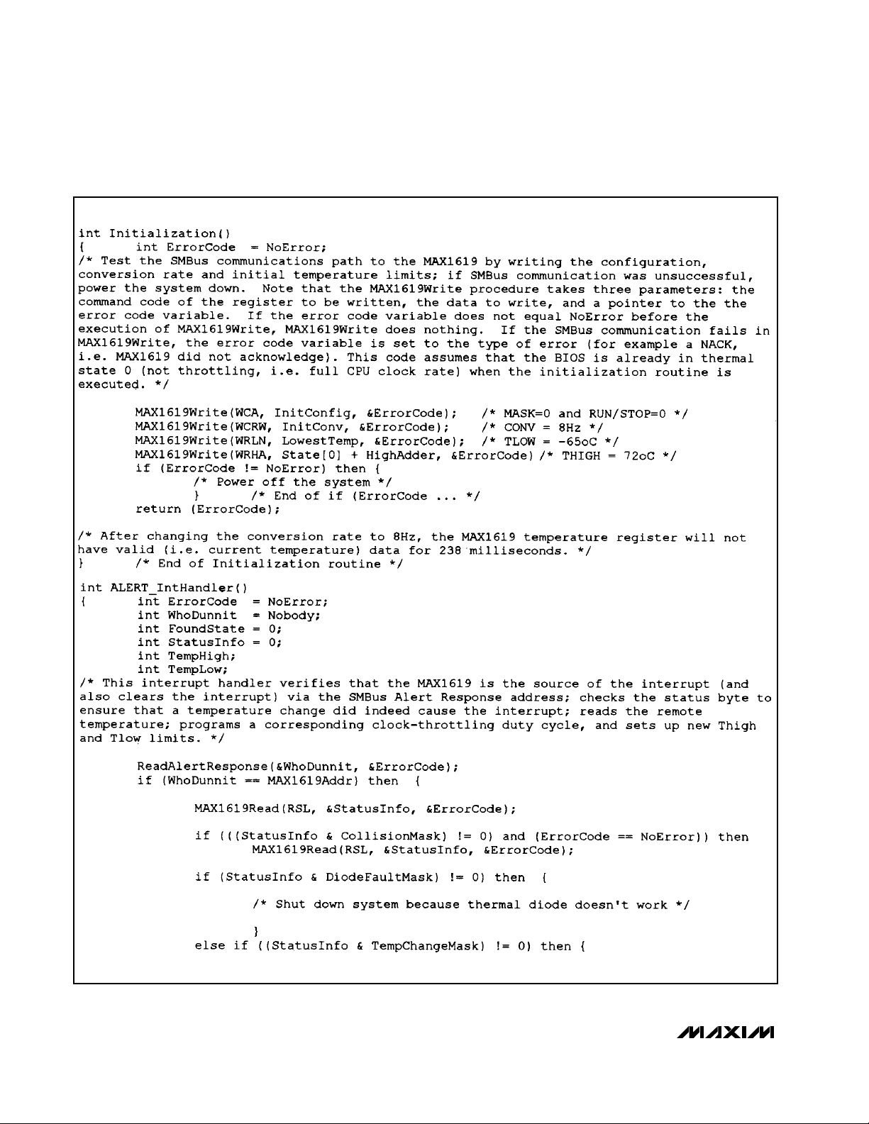
Programming Example:
Clock-Throttling Control for CPUs
Listing 1 gives an untested example of pseudocode for
proportional temperature control of Intel mobile CPUs
through a power-management microcontroller. This
program consists of two main parts: an initialization routine and an interrupt handler. The initialization routine
checks for SMBus communications problems and sets
up the MAX1619 configuration and conversion rate. The
interrupt handler responds to ALERT signals by reading
the current temperature and setting a CPU clock duty
factor proportional to that temperature. The relationship
between clock duty and temperature is fixed in a lookup table contained in the microcontroller code.
Note: Thermal management decisions should be made
based on the latest external temperature obtained from
the MAX1619 rather than the value of the Status Byte.
The MAX1619 responds very quickly to changes in its
environment due to its sensitivity. High and low alarm
conditions can exist at the same time in the Status Byte
due to the MAX1619 correctly reporting environmental
changes around it.
Chip Information
TRANSISTOR COUNT: 11,487
Page 20

Maxim cannot assume responsibility for use of any circuitry other than circuitry entirely embodied in a Maxim product. No circuit patent licenses are
implied. Maxim reserves the right to change the circuitry and specifications without notice at any time.
20
__________________Maxim Integrated Products, 120 San Gabriel Drive, Sunnyvale, CA 94086 (408) 737-7600
© 1999 Maxim Integrated Products Printed USA is a registered trademark of Maxim Integrated Products.
MAX1619
Remote/Local Temperature Sensor with DualAlarm Outputs and SMBus Serial Interface
Package Information
QSOP.EPS
 Loading...