

Page 1
________________General Description
The MAX1618 precise digital thermometer reports the
temperature of a remote sensor. The remote sensor is a
diode-connected transistor—typically a low-cost, easily
mounted 2N3904 NPN type—that replaces conventional
thermistors or thermocouples. Remote accuracy is ±3°C
for multiple transistor manufacturers, with no calibration
needed. The MAX1618 can also measure the die temperature of other ICs, such as microprocessors, that contain
an on-chip, diode-connected transistor.
The 2-wire serial interface accepts standard System
Management Bus (SMBus™) Write Byte, Read Byte, Send
Byte, and Receive Byte commands to program the alarm
thresholds and to read temperature data. The data format
is 7 bits plus sign, with each bit corresponding to 1°C, in
two’s complement format. Measurements can be done
automatically and autonomously, with the 16Hz conversion
rate or programmed to operate in a single-shot mode.
The thermostat mode configures the ALERT output as an
interrupt or as a temperature reset that remains active only
while the temperature is above the maximum temperature
limit or below the minimum temperature limit. The ALERT
output polarity in thermostat mode can be configured for
active high or active low. Fan control is implemented using
this ALERT output.
The MAX1618 is available in a small (1.1mm high) 10-pin
µMAX package.
________________________Applications
Desktop and Notebook Central Office
Computers Telecom Equipment
Smart Battery Packs Test and Measurement
LAN Servers Multichip Modules
Industrial Controls
____________________________Features
♦ Single Channel: Measures Remote CPU
Temperature
♦ No Calibration Required
♦ SMBus 2-Wire Serial Interface
♦ Programmable Under/Overtemperature Alarms
♦ Overtemperature Output for Fan Control
(Thermostat Mode)
♦ Supports SMBus Alert Response Accuracy
±3°C (+60°C to +100°C)
±5°C (-55°C to +120°C)
♦ 3µA (typ) Standby Supply Current
♦ 900µA (max) Supply Current in Autoconvert Mode
♦ +3V to +5.5V Supply Range
♦ Small 10-Pin µMAX Package
MAX1618
†
Remote Temperature Sensor
with SMBus Serial Interface
________________________________________________________________ Maxim Integrated Products 1
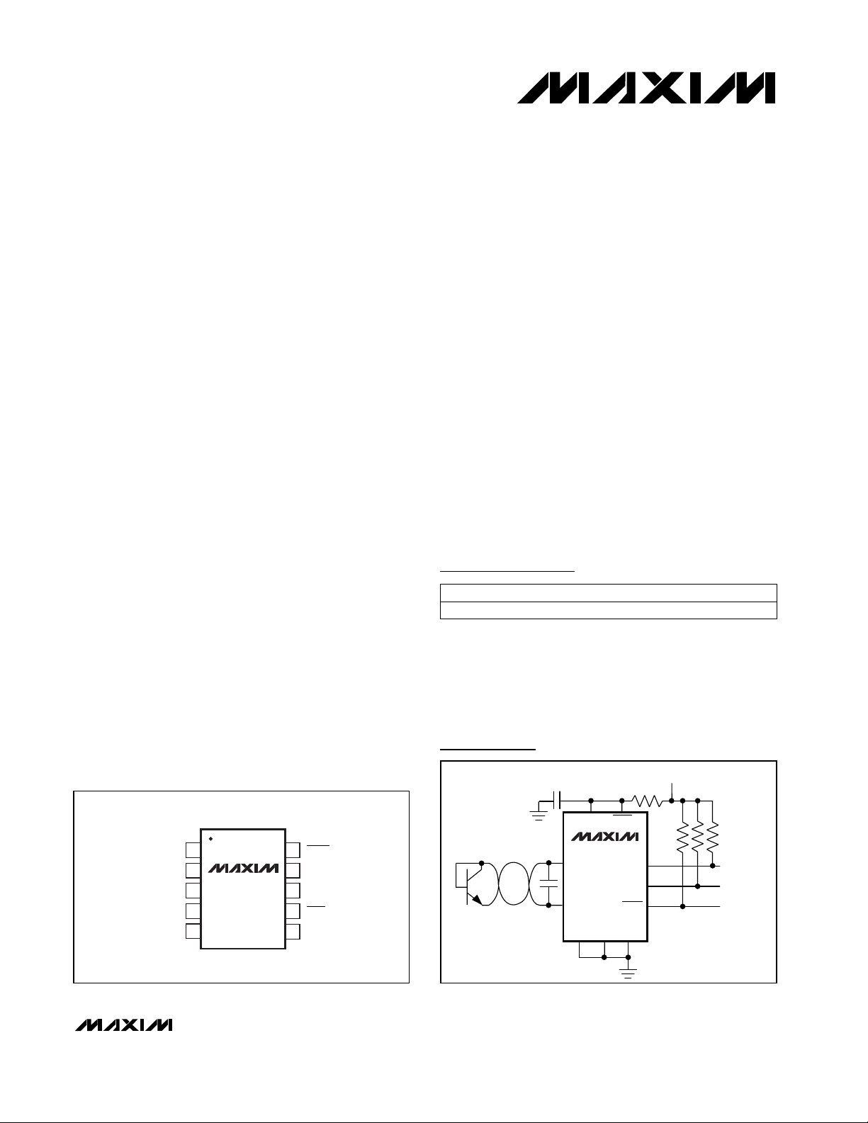
___________________Pin Configuration
1
2
3
4
5
10
9
8
7
6
ALERT
SMBDATA
SMBCLK
STBYDXN
GND
ADD1
ADD0
MAX1618
µMAX
TOP VIEW
V
CC
DXP
Typical Operating Circuit
19-1495; Rev 1; 12/99
PART
MAX1618MUB -55°C to +125°C
TEMP. RANGE PIN-PACKAGE
10 µMAX
Ordering Information
SMBus is a trademark of Intel Corp.
†Patents Pending
For pricing, delivery, and ordering information, please contact Maxim/Dallas Direct! at
1-888-629-4642, or visit Maxim’s website at www.maxim-ic.com.
2N3904
0.1µF
2200pF
V
CC
MAX1618
DXP
DXN
ADD0 ADD1
SMBDATA
3V TO 5.5V
200Ω
STBY
SMBCLK
ALERT
GND
10k EACH
CLOCK
DATA
INTERRUPT
TO µC
Page 2
Autoconvert
mode, average
MAX1618
Remote Temperature Sensor
with SMBus Serial Interface
2 _______________________________________________________________________________________
ABSOLUTE MAXIMUM RATINGS
ELECTRICAL CHARACTERISTICS
(VCC= +3.3V, configuration byte register = X8h, TA= 0°C to +85°C, unless otherwise noted.)
Stresses beyond those listed under “Absolute Maximum Ratings” may cause permanent damage to the device. These are stress ratings only, and functional
operation of the device at these or any other conditions beyond those indicated in the operational sections of the specifications is not implied. Exposure to
absolute maximum rating conditions for extended periods may affect device reliability.
VCCto GND..............................................................-0.3V to +6V
DXP, ADD_ to GND ....................................-0.3V to (V
CC
+ 0.3V)
DXN to GND ..........................................................-0.3V to +0.8V
SMBCLK, SMBDATA, ALERT, STBY to GND ...........-0.3V to +6V
SMBDATA Current.................................................-1mA to 50mA
DXN Current. ......................................................................±1mA
ESD Protection (all pins, Human Body Model).. .............± 2000V
Continuous Power Dissipation (T
A
= +70°C)
µMAX (derate 5.6mW/°C above +70°C) ....................444mW
Operating Temperature Range (extended)......-55°C to +125°C
Junction Temperature.....................................................+150°C
Storage Temperature Range ............................-65°C to +150°C
Lead Temperature (soldering, 10s) ................................+300°C
CONDITIONSSYMBOL UNITSMIN TYP MAXPARAMETER
Monotonicity guaranteed Bits
8
Temperature Resolution
(Note 1)
V
CC
V
3 5.5
Supply-Voltage Range
TR= +60°C to +100°C
°C
-3 3
Temperature Error,
Remote Diode (Note 2)
mV
50
Undervoltage Lockout Hysteresis
VCCinput, disables A/D conversion,
rising edge
mV
50
POR Threshold Hysteresis
VCC, falling edge V
1 1.7 2.5
Power-On Reset Threshold
UVLO V
2.6 2.8 2.95
Undervoltage Lockout
Threshold
Hardware or software standby,
SMBCLK at 10kHz
µA
5
Standby Supply Current
From stop bit to conversion complete
SMBus static
t
CONV
ms
47 62 78
Conversion Time
µA
450 900
Average Operating
Supply Current
µA
80 100 120
Remote-Diode Source Current
Autoconvert mode
V
0.7
DXN Source Voltage
81012
%
-25 25
Conversion Rate Timing Error
µA
310
Standby Supply Current
VCC= 3.0V to 5.5V
Momentary upon power-on reset
V
IL
V
0.8
STBY,
SMBCLK, SMBDATA
Input Low Voltage
VCC= 3.0V V
IH
V
2.2
STBY SMBCLK, SMBDATA
Input High Voltage
SMBCLK, SMBDATA forced to 0.4V mA
6
SMBCLK, SMBDATA
Output Low Sink Current
Logic inputs forced to VCCor GND µA
-1 1
STBY,
SMBCLK, SMBDATA
Input Current
µA
160
ADDO, ADD1 Bias Current
TR= +55°C to +125°C
-5 5
Autoconvert mode, average measured over
4sec, 16 conv/sec
DXP forced to DXN + 0.65V,
ID = 1 (high)
High level
Low level
SMBus INTERFACE
ADC AND POWER SUPPLY
Page 3
MAX1618
Remote Temperature Sensor
with SMBus Serial Interface
_______________________________________________________________________________________ 3
ELECTRICAL CHARACTERISTICS (continued)
(VCC= +3.3V, configuration byte register = X8h, TA= 0°C to +85°C, unless otherwise noted.)
ELECTRICAL CHARACTERISTICS
(VCC= +3.3V, configuration byte register = X8h, TA= -55°C to +125°C, unless otherwise noted.) (Note 5)
CONDITIONS
Monotonicity guaranteed
TR= +60°C to +100°C
Bits8Temperature Resolution (Note 1)
-3 3
TR= -55°C to +125°C
°C
-5 5
Initial Temperature Error,
Remote Diode (Note 2)
V3 5.5Supply-Voltage Range
From stop bit to conversion complete
Autoconvert mode
ms47 62 78Conversion Time
%-25 25Conversion-Rate Timing Error
UNITSMIN TYP MAXPARAMETER
CONDITIONSSYMBOL
ALERT forced to 5.5V
µA
1
ALERT Output High
Leakage Current
ALERT forced to 0.4V
mA
6
ALERT Output Low Sink Current
UNITSMIN TYP MAXPARAMETER
(Note 3) kHz
DC 100
SMBus Clock Frequency
90% to 90% points t
HIGH
µs
4
SMBCLK Clock High Time
10% to 10% points t
LOW
µs4.7SMBCLK Clock Low Time
90% to 10% pointst
F
ns
300
SMBCLK, SMBDATA Fall Time
90% to 90% points
10% to 90% points
t
SU:STA
ns
500
SMBus Repeated Start
Condition Setup Time
µs
4.7
SMBus Start Condition
Setup Time
t
R
µs
1
SMBCLK, SMBDATA Rise Time
pF
5
SMBCLK, SMBDATA Input
Capacitance
90% of SMBCLK to 10% of SMBDATAt
SU:STO
µs
4
SMBus Stop Condition
Setup Time
(Note 4)
10% of SMBDATA to 90% of SMBCLK
t
HD:DAT
µs
0
SMBus Data-Hold Time
90% of SMBDATA to 10% of SMBCLKt
SU:DAT
ns
250
SMBus Data Valid to SMBCLK
Rising-Edge Time
t
HD:STA
µs
4
SMBus Start Condition
Hold Time
Master clocking in data µs
1
SMBCLK Falling Edge to SMBus
Data-Valid Time
Between start/stop condition t
BUF
µs
4.7
SMBus Bus Free Time
V
CC
t
CONV
SYMBOL
Page 4
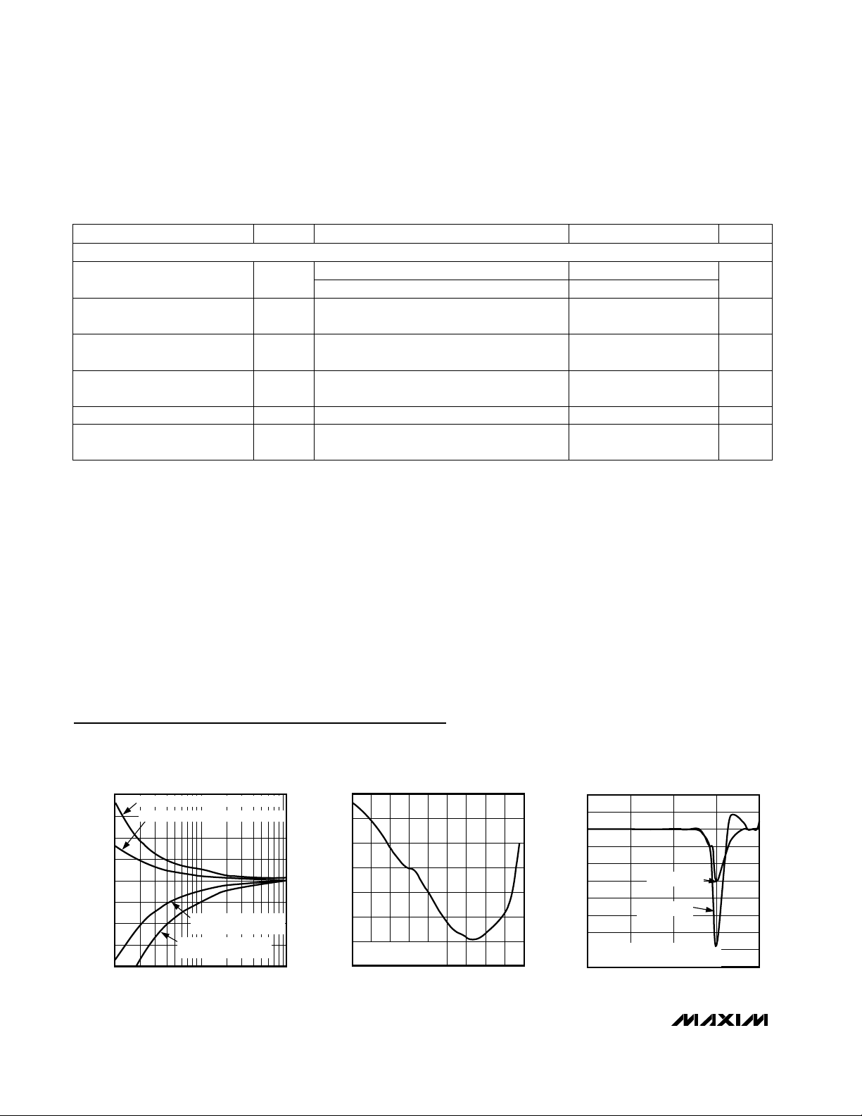
40
-40
1 100
TEMPERATURE ERROR
vs. LEAKAGE RESISTANCE
-20
-30
-10
0
10
20
30
MAX1618 toc01
LEAKAGE RESISTANCE (MΩ)
TEMPERATURE ERROR (°C)
10
PATH = DXP TO GND AND CONFIG = H00
PATH = DXP TO GND AND CONFIG = H08
PATH = DXP TO VCC (5.0V)
AND CONFIG = H08
PATH = DXP TO VCC (5.0V)
AND CONFIG = H00
-8
-5
-6
-7
-4
-3
-2
-1
0
1
2
0.005 0.05 0.5 5 50
TEMPERATURE ERROR vs.
POWER-SUPPLY NOISE FREQUENCY
MAX1618 toc03
POWER-SUPPLY NOISE FREQUENCY (MHz)
TEMPERATURE ERROR (°C)
VIN = SQUARE WAVE APPLIED TO
V
CC
WITH NO 0.1µF VCC CAPACITOR
VIN = 100mVp-p
VIN = 250mVp-p
Typical Operating Characteristics
(TA = +25°C, unless otherwise noted.)
-1.00
0.00
-0.50
1.00
0.50
2.00
1.50
2.50
-55 -15 5-35 25 45 65 85 105 125
TEMPERATURE ERROR
vs. REMOTE-DIODE TEMPERATURE
MAX1618 toc02
TEMPERATURE (°C)
TEMPERATURE ERROR (°C)
CENTRAL CMPT3904
RANDOM SAMPLE
MAX1618
Remote Temperature Sensor
with SMBus Serial Interface
4 _______________________________________________________________________________________
ELECTRICAL CHARACTERISTICS (continued)
(VCC= +3.3V, configuration byte register = X8h, TA= -55°C to +125°C, unless otherwise noted.) (Note 5)
Note 1: Guaranteed, but not 100% tested.
Note 2: A remote diode is any diode-connected transistor from Table 7. T
R
is the junction temperature of the remote diode. See
Remote Diode Selection for remote-diode forward voltage requirements. Temperature specification guaranteed for a diode
with ideality factor (M
TR
= 1.013). Additional error = (1.013/M - 1) ✕273 + Temp where M = Ideality of remote diode used.
Note 3: The SMBus logic block is a static design that works with clock frequencies down to DC. While slow operation is possible, it
violates the 10kHz minimum clock frequency and SMBus specifications and may monopolize the bus.
Note 4: Note that a transition must internally provide at least a hold time to bridge the undefined region (300ns max) of SMBCLK’s
falling edge.
Note 5: Specifications from -55°C to +125°C are guaranteed by design, not production tested.
CONDITIONS UNITSMIN TYP MAXPARAMETER
VCC= 3.0V 2.2
STBY, SMBCLK, SMBDATA
Input High Voltage
V
2.4
ALERT forced to 0.4V
mA1
ALERT Output Low Sink Current
VCC= 5.5V
VCC= 3.0V to 5.5V 0.8
STBY, SMBCLK, SMBDATA
Input Low Voltage
V
Logic inputs forced to VCCor GND -2 2
STBY, SMBCLK, SMBDATA
Input Current
µA
SMBCLK, SMBDATA forced to 0.6V 6
SMBCLK, SMBDATA Output
Low Sink Current
mA
ALERT forced to 5.5V
µA1
ALERT Output High Leakage
Current
SMBus INTERFACE
Page 5
MAX1618
Remote Temperature Sensor
with SMBus Serial Interface
_______________________________________________________________________________________ 5
____________________________Typical Operating Characteristics (continued)
(TA = +25°C, unless otherwise noted.)
120
100
80
60
40
TEMPERATURE ERROR (°C)
20
TEMPERATURE ERROR vs.
COMMON-MODE NOISE FREQUENCY
AC-COUPLED TO DXN
2200pF DXN-DXP CAPACITOR
VIN = 100mVp-p
VIN = 50mVp-p
0
10 100 1000
COMMON-MODE NOISE FREQUENCY (MHz)
MAX1618 toc04
STANDBY SUPPLY CURRENT
vs. CLOCK FREQUENCY
50
40
30
VCC = 5V
TEMPERATURE ERROR
vs. DXP-DXN CAPACITANCE
0
-10
TEMPERATURE ERROR (°C)
-20
0806020 40 100
DXP-DXN CAPACITANCE (nF)
MAX1618 toc06
VCC = 5V
MAX1618 toc05
20
10
STANDBY SUPPLY CURRENT (µA)
0
1 10 100 1000
CLOCK FREQUENCY (kHz)
VCC = 3.3V
STANDBY SUPPLY CURRENT
100
90
80
70
60
50
40
30
20
STANDBY SUPPLY CURRENT (µA)
10
0
vs. SUPPLY VOLTAGE
ADD0, ADD1 = GND
ADD0, ADD1 = HIGH-Z
021 345
SUPPLY VOLTAGE (V)
MAX1618 toc07
TEMPERATURE (°C)
RESPONSE TO THERMAL SHOCK
120
110
100
90
80
70
60
50
40
30
20
-2 2 40 6 8 101214161820
10-PIN µMAX IMMERSED IN
+115°C FLUORINERT BATH
TIME (sec)
MAX1618 toc08
Page 6
MAX1618
Remote Temperature Sensor
with SMBus Serial Interface
6 _______________________________________________________________________________________
Pin Description
Detailed Description
The MAX1618 is a temperature sensor designed to
work in conjunction with an external microcontroller
(µC) or other intelligence in thermostatic, process-control, or monitoring applications. The µC is typically a
power-management or keyboard controller, generating
SMBus serial commands by “bit-banging” general-purpose input-output (GPIO) pins or through a dedicated
SMBus interface block.
Essentially an 8-bit serial analog-to-digital converter
(ADC) with a sophisticated front end, the MAX1618
contains a switched-current source, a multiplexer, an
ADC, an SMBus interface, and the associated control
logic (Figure 1). Temperature data from the ADC is
loaded into a data register, where it is automatically
compared with data previously stored in over/undertemperature alarm threshold registers. The alarm
threshold registers can be set for hysteretic fan control.
ADC and Multiplexer
The averaging ADC integrates over a 30ms period (typ)
with excellent noise rejection. The ADC converts at a
rate of 16Hz. The multiplexer automatically steers bias
currents through the remote diode, measures the forward voltage, and computes the temperature.
The DXN input is biased at 0.65V above ground by an
internal diode to set up the analog-to-digital (A/D)
inputs for a differential measurement. The worst-case
DXP-DXN differential input voltage range is 0.25V to
0.95V.
Excess resistance in series with the remote diode
causes about +1/2°C error/Ω. A 200µV offset voltage at
DXP-DXN causes about +1°C error.
A/D Conversion Sequence
If a Start command is written (or generated automatically in the free-running autoconvert mode), the result of
the measurement is available after the end of conversion. A BUSY status bit in the status byte shows that the
device is performing a new conversion. The result of the
previous conversion is always available even when the
ADC is busy.
SMBus Serial-Data Input/Output. Open drain.SMBDATA9
SMBus Alert (Interrupt) Output. Open drain.
ALERT
10
Combined Current Source and A/D Positive Input. Do not leave DXP floating. Place a 2200pF capacitor
between DXP and DXN for noise filtering.
DXP5
Supply Voltage Input. Bypass to GND with a 0.1µF capacitor.V
CC
6
Hardware-Standby Input. Temperature and comparison threshold data are retained in standby mode.
Low = standby mode. High = operating mode.
STBY
7
SMBus Serial-Clock InputSMBCLK8
Combined Current Sink and A/D Negative Input. DXN is normally biased to a diode voltage above
ground.
DXN4
GroundGND3
PIN
SMBus Slave Address Select Input. (See Table 6.) ADD0 and ADD1 are sampled upon power-up. Excess
capacitance (>50pF) at the address pins when floating may cause address-recognition problems.
ADD12
SMBus Slave Address Select Input. (See Table 6.) ADD0 and ADD1 are sampled upon power-up. Excess
capacitance (>50pF) at the address pins when floating may cause address-recognition problems.
ADD01
FUNCTIONNAME
Page 7

MAX1618
Remote Temperature Sensor
with SMBus Serial Interface
_______________________________________________________________________________________ 7
Figure 1. Functional Diagram
MUX
REMOTE-TEMPERATURE
DATA REGISTER
HIGH-TEMPERATURE
THRESHOLD
LOW-TEMPERATURE
THRESHOLD
DIGITAL COMPARATOR
COMMAND-BYTE
(INDEX) REGISTER
SMBDATA
SMBCLK
ADDRESS
DECODER
READ WRITE
CONTROL
LOGIC
CONTROL
LOGIC
SMBUS
ADD1
ADD0
STBY
STATUS BYTE REGISTER
CONFIGURATION
BYTE REGISTER
ALERT RESPONSE
ADDRESS REGISTER
ADC
+
DXP
DXN
GND
V
CC
-
+
-
8
8
8
88
ALERT
MAX1618
SQ
R
Page 8

Low-Power Standby Mode
Standby mode disables the ADC and reduces the supply-current drain to 3µA (typ). Enter standby mode by
forcing the STBY pin low or through the RUN/STOP bit in
the configuration-byte register. Hardware and software
standby modes behave almost identically; all data is
retained in memory, and the SMB interface is alive and
listening for reads and writes. The only difference is that
in hardware-standby mode, the one-shot command
does not initiate a conversion.
Standby mode is not a shutdown mode. Activity on the
SMBus draws extra supply current (see Typical
Operating Characteristics). In software-standby mode,
the MAX1618 can be forced to perform A/D conversions
through the one-shot command, despite the RUN/STOP
bit being high.
Enter hardware standby mode by forcing the STBY pin
low. In a notebook computer, this line may be connected to the system SUSTAT# suspend-state signal.
The STBY pin low state overrides any software conversion command. If a hardware- or software-standby command is received while a conversion is in progress, the
conversion cycle is truncated, and the data from that
conversion is not latched into either temperature-reading register. The previous data is not changed and
remains available.
Supply-current drain during the 62ms conversion period
is always about 450µA. Between conversions, the
instantaneous supply current is about 25µA due to the
current consumed by the conversion-rate timer. In
standby mode, supply current drops to about 3µA. With
very low supply voltages (under the power-on reset
threshold), the supply current is higher due to the
address input bias currents. It can be as high as 160µA,
depending on ADD0 and ADD1 settings.
SMBus Digital Interface
From a software perspective, the MAX1618 appears as a
set of byte-wide registers that contains temperature data,
alarm threshold values, or control bits. Use a standard
SMBus 2-wire serial interface to read temperature data
and write control bits and alarm threshold data.
The MAX1618 employs four standard SMBus protocols:
Write Byte, Read Byte, Send Byte, and Receive Byte
(Figure 2). The two shorter protocols (Receive and Send)
allow quicker transfers, provided that the correct data
register was previously selected by a Write or Read Byte
instruction. Use caution with the shorter protocols
in multimaster systems, since a second master could
overwrite the command byte without informing the first
master.
The temperature data format is 7 bits plus sign in two’s
complement form for each channel, with each data bit
representing +1°C (Table 1), transmitted MSB first.
Measurements are offset by +1/2°C to minimize internal
rounding errors; for example, +99.6°C is reported as
+100°C.
Alarm Threshold Registers
Two registers, a high-temperature (T
HIGH
) and a low-
temperature (T
LOW
) register, store alarm threshold
data. If a measured temperature equals or exceeds the
corresponding alarm threshold value, an ALERT interrupt is asserted.
The power-on reset (POR) state of the T
HIGH
register is
full scale (0111 1111 or +127°C). The POR state of the
T
LOW
register is 1100 1001 or -55°C.
Thermostat Mode
Thermostat mode changes the function of the ALERT
output from a latched interrupt-type output to a selfclearing thermostat for fan control. This output simply
responds to the current temperature (Figure 3). If the
current temperature is above T
HIGH
, ALERT activates
MAX1618
Remote Temperature Sensor
with SMBus Serial Interface
8 _______________________________________________________________________________________
Table 1. Data Format (Two’s Complement)
DIGITAL OUTPUT
DATA BITS
0 111 1111+127+127.00
0 111 1111
0 111 1111+126+126.00
+127+126.50
0 001 1001
0 000 0001+1+0.50
0 000 0000
0 000 000000.00
ROUNDED
TEMP.
(°C)
TEMP.
(°C)
0+0.25
+25+25.25
0 000 0000
0 000 00000-0.50
1 111 1111
1 111 1111-1-1.00
-1-0.75
1 110 0111
1 110 0111-25-25.50
1 100 1001
1 100 1001-55-55.00
0-0.25
-55-54.75
-25-25.00
1 011 1111
1 011 1111-65-70.00
-65-65.00
SIGN MSB LSB
0 111 1111+127+130.00
Page 9

and does not go inactive until the temperature drops
below T
LOW
.
Enable thermostat mode through the configuration register (Table 4), with one bit to enable the feature and
another bit to set the output polarity (active high or
active low). The ALERT thermostat comparison is made
after each conversion, or at the end of any SMBus
transaction. For example, if the limit is changed while
the device is in standby mode, the ALERT output
responds correctly according to the last valid A/D
result. Upon entering thermostat mode, the ALERT out-
put is reset so that if the temperature is in the hysteresis
band ALERT initially goes inactive. The power-on reset
(POR) state disables thermostat mode.
Diode Fault Alarm
A continuity fault detector at DXP detects whether the
remote diode has an open-circuit condition, short-circuit to GND, or short-circuit DXP-to-DXN condition. At
the beginning of each conversion, the diode fault is
checked, and the status byte is updated. This fault
detector is a simple voltage detector; if DXP rises
MAX1618
Remote Temperature Sensor
with SMBus Serial Interface
_______________________________________________________________________________________ 9
Figure 3. Fan Control Application
Write Byte Format
Read Byte Format
Send Byte Format Receive Byte Format
Slave Address: equivalent to chip-select line of
a 3-wire interface
Command Byte: selects which
register you are writing to
Data Byte: data goes into the register
set by the command byte (to set
thresholds, configuration masks, and
sampling rate)
Slave Address: equivalent to chip-select line of
a 3-wire interface
Command Byte: selects
which register you are
reading from
Slave Address: repeated
due to change in dataflow direction
Data Byte: reads from
the register set by the
command byte
Data Byte: writes data to the
register commanded by the
last Read Byte or Write Byte
transmission
Data Byte: reads data from
the register commanded
by the last Read Byte or
Write Byte transmission;
also used for SMBus Alert
Response return address
S = Start condition Shaded = Slave transmission
P = Stop condition
A
= Not acknowledged
Figure 2. SMBus Protocols
S ADDRESS
7 bits
WR
ACK DATA
8 bits
ACK P S ADDRESS
7 bits
WR
ACK DATA
8 bits
A
P
S ADDRESS
7 bits
WR
ACK COMMAND
8 bits
ACK S ADDRESS
7 bits
RD ACK DATA
8 bits
A
P
S ADDRESS
7 bits
WR
ACK
8 bits
COMMAND ACK
8 bits
DATA ACK P
+3V TO +5.5V
STBY V
CC
+12V
SMBUS
SERIAL
INTERFACE
(TO HOST)
MAX1618
SMBCLK
SMBDATA
DXP
2N3904
DXN
ADD0
ADD1
ALERT
GND
Page 10

above VCC- 1V (typ) or below V
DXN
+ 50mv (typ), a
fault is detected and ALERT is asserted. ADC reads
+127°C. Also, if the ADC has an extremely low differential input voltage, the diode is assumed to be shorted
and a fault is detected. Note that the diode fault is not
checked until a conversion is initiated, so immediately
after power-on reset, the status byte indicates no fault
is present even if the diode path is broken.
AALLEERRTT
Interrupts
Normally, the ALERT interrupt output signal is latched
and can be cleared only by reading the Alert Response
address. Interrupts are generated in response to T
HIGH
and T
LOW
comparisons and when the remote diode is
faulted. The interrupt does not halt automatic conversions; new temperature data continues to be available
over the SMBus interface after ALERT is asserted. The
interrupt output pin is open-drain so the devices can
share a common interrupt line.
The interface responds to the SMBus Alert Response
address, an interrupt pointer return-address feature
(see Alert Response Address section). Before taking
corrective action, always check to ensure that an interrupt is valid by reading the current temperature.
The alert activates only once per crossing of a given
temperature threshold to prevent any re-entrant interrupts. To enable a new interrupt, rewrite the value of the
violated temperature threshold.
Alert Response Address
The SMBus Alert Response interrupt pointer provides
quick fault identification for simple slave devices that
lack the complex, expensive logic needed to be a bus
master. Upon receiving an ALERT interrupt signal, the
host master can broadcast a Receive Byte transmission
to the Alert Response slave address (0001100). Any
slave device that generated an interrupt then attempts
to identify itself by putting its own address on the bus
(Table 2).
The Alert Response can activate several different slave
devices simultaneously, similar to the I2C General Call.
If more than one slave attempts to respond, bus arbitration rules apply, and the device with the lower address
code wins. The losing device does not generate an
acknowledgement and continues to hold the ALERT
line low until serviced (implies that the host interrupt
input is level sensitive). Successful reading of the alert
response address clears the interrupt latch.
Command Byte Functions
The 8-bit command byte register (Table 3) is the master
index that points to the other registers within the
MAX1618. The register’s POR state is 0000 0001, so a
Receive Byte transmission (a protocol that lacks the
command byte) that occurs immediately after POR
returns the current remote temperature data.
The one-shot command immediately forces a new conversion cycle to begin. A new conversion begins in
software standby mode (RUN/STOP bit = high). The
device returns to standby mode after the conversion. If
a conversion is in progress when a one-shot command
is received, the command is ignored. If a one-shot
command is received in autoconvert mode (RUN/STOP
bit = low) between conversions, a new conversion
begins; the conversion rate timer is reset, and the next
automatic conversion takes place after a full delay
elapses.
Configuration Byte Functions
The configuration byte register (Table 4) is used to
mask (disable) interrupts, to put the device in softwarestandby or thermostat mode, change the polarity of the
alert output (thermostat mode only), and to change the
diode bias current. The lower three bits are internally
driven low (000), making them “don’t care” bits. Write
zeros to these bits. The serial interface can read back
this register’s contents.
Status Byte Functions
The status byte register (Table 5) indicates which (if
any) temperature thresholds have been exceeded. This
byte also indicates whether the ADC is converting and
whether there is a fault in the remote diode DXP-DXN
path. After POR, the normal state of all the flag bits is
zero, assuming none of the alarm conditions is present.
The status byte is cleared by any successful read of
the status byte. Note that the ALERT interrupt latch is
not automatically cleared when the status flag bit is
cleared.
MAX1618
Remote Temperature Sensor
with SMBus Serial Interface
10 ______________________________________________________________________________________
ADD66
Provide the current MAX1618
slave address that was latched at
POR (Table 6)
FUNCTION
ADD55
ADD44
ADD33
ADD22
ADD11
ADD7
7
(MSB)
ADD0
0
(LSB)
Logic 1
BIT NAME
Table 2. Read Format for Alert Response
Address (0001 100)
I2C is a trademark of Philips Corp.
Page 11

MAX1618
Remote Temperature Sensor
with SMBus Serial Interface
______________________________________________________________________________________ 11
Read remote temperature; returns latest temperatureRRTE 01h
00h
COMMAND
0000 0000*
N/A
POR STATE
Read configuration byteRCL 03h
02h
0000 1000
N/A Read status byte (flags, busy signal)RSL
Reserved for future useRFU 05h
Reserved for future useRFU
04h
N/A
0000 0111
Read remote T
HIGH
limitRRHI 07h
06h
0111 1111
N/A Reserved for future useRFU
Read conversion rate byte (not supported by MAX1618)
REGISTER
RCRA
Write configuration byteWCA 09h
08h
N/A
1100 1001
FUNCTION
Reserved for future useRFU 0Bh
0Ah
N/A
N/A Write conversion rate byte (not supported by MAX1618)WCRW
Write remote T
HIGH
limitWRHA 0Dh
Read remote T
LOW
limitRRLS
0Ch
N/A
N/A
One-shot commandOSHT 0Fh
0Eh
N/A
N/A Write remote T
LOW
limitWRLN
Reserved for future useRFU
Read device ID codeDEVID FFh
FEh
00000010
01001101 Read manufacturer ID codeMFGID
*If the device is in hardware-standby mode at POR, the temperature register reads 0°C.
Table 3. Command-Byte Bit Assignments
Table 4. Configuration-Byte Bit
Assignments
RUN/
STOP
6 0
0
POR
STATE
Standby mode control bit. If
high, the device immediately
stops converting and enters
standby mode. If low, the
device converts in either
one-shot or timer mode.
Masks all ALERT interrupts
when high.
FUNCTION
POL5 0
ALERT pin polarity control in
thermostat mode.
0 = active low
1 = active high
THERM4 0
Enables thermostat mode
when high.
ID3 1
MASK
7
(MSB)
Enables diode bias current.
0 (Logic Low) = 5µA to 50µA
(typ)
1 (Logic High) = 10µA to
100µA (typ)
2 to 0 RFU 0 Reserved for future use.
BIT NAME
RFU6, 5 Reserved for future use (returns 0).
A high indicates that the ADC is busy
converting.
FUNCTION
RHIGH*4
A high indicates that the remote hightemperature alarm has activated. In
thermostat mode, this bit is always in
the same state as the ALERT output.
RLOW* 3
A high indicates that the remote lowtemperature alarm has activated. In
thermostat mode, this bit is always
zero.
DIODE2
A high indicates a remote-diode fault
(open-circuit, shorted diode, or DXP
short to GND).
RFU
1, 0
(LSB)
Reserved for future use (returns 0).
BUSY
7
(MSB)
BIT NAME
Table 5. Status-Byte Bit
Assignments
*In
ALERT
mode, the HIGH and LOW temperature alarm flags
stay high until cleared by POR or until the status byte register
is read.
Page 12

Slave Addresses
The device address can be set to one of nine different
values by pin-strapping ADD0 and ADD1 so more than
one MAX1618 can reside on the same bus without
address conflicts (Table 6).
The address pin states are checked at POR only, and
the address data stays latched to reduce quiescent
supply current due to the bias current needed for highimpedance (high-Z) state detection.
The MAX1618 also responds to the SMBus Alert
Response slave address (see the Alert Response
Address section).
POR and UVLO
The MAX1618 has a volatile memory. To prevent ambiguous power-supply conditions from corrupting the data in
the memory and causing erratic behavior, a POR voltage
detector monitors VCCand clears the memory if VCCfalls
below 1.7V (typical, see the Electrical Characteristics
table). When power is first applied and VCCrises above
1.75V (typ), the logic blocks begin operating, although
reads and writes at VCClevels below 3V are not recommended. A second VCCcomparator, the ADC UVLO comparator, prevents the ADC from converting until there is
sufficient headroom (VCC= 2.8V typ).
Power-Up Defaults:
• Interrupt latch is cleared.
• Address select pins are sampled.
• Command byte is set to 01h to facilitate quick
remote Receive Byte queries.
• T
HIGH
and T
LOW
registers are set to max and min
limits, respectively.
• Device is in normal mode. (ALERT acts as a latched
interrupt output.)
Applications Information
Remote Diode Selection
Temperature accuracy depends on having a goodquality, diode-connected, small-signal transistor.
Accuracy has been experimentally verified for all of the
devices listed in Table 7. The MAX1618 can also directly measure the die temperature of CPUs and other integrated circuits with on-board temperature sensing
diodes, such as the Intel Pentium II®.
The transistor must be a small-signal type with a relatively high forward voltage. This ensures that the input
voltage is within the A/D input voltage range. The forward voltage must be greater than 0.25V at 10µA at the
highest expected temperature. The forward voltage
must be less than 0.95V at 100µA at the lowest expected temperature. The base resistance has to be less
than 100Ω. Tight specification of forward-current gain
(+50 to +150, for example) indicates that the manufacturer has good process controls and that the devices
have consistent VBEcharacteristics. Do not use power
transistors.
ADC Noise Filtering
The integrating ADC has inherently good noise rejection, especially of low-frequency signals such as
60Hz/120Hz power-supply hum. Micropower operation
places constraints on high-frequency noise rejection.
Lay out the PCB carefully with proper external noise filtering for high-accuracy remote measurements in electrically noisy environments.
Filter high-frequency electromagnetic interference
(EMI) at DXP and DXN with an external 2200pF capacitor connected between the two inputs. This capacitor
can be increased to about 3300pF (max), including
cable capacitance. A capacitance higher than 3300pF
MAX1618
Remote Temperature Sensor
with SMBus Serial Interface
12 ______________________________________________________________________________________
0011 001High-ZGND
0011 000
ADDRESS
0101 001GNDHigh-Z
0011 010V
CC
GND
0101 011V
CC
High-Z
0101 010
1001 101High-ZV
CC
1001 100
GNDGND
GNDV
CC
High-ZHigh-Z
1001 110V
CC
V
CC
ADD0 ADD1
Table 6. Slave Address Decoding
(ADD0 and ADD1)
Note: High-Z means the pin is left unconnected and floating.
Note: Transistors must be diode-connected (short the base to
the collector).
SMBT3904Siemens (Germany)
CMPT3904Central Semiconductor (USA)
MMBT3904Fairchild Semiconductor (USA)
SST3904Rohm Semiconductor (Japan)
FMMT3904CT-NDZetex (England)
MANUFACTURER MODEL NUMBER
Table 7. SOT23 Type Remote-Sensor
Transistor Manufacturers
MMBT3904Motorola (USA)
Pentium II is a registered trademark of Intel Corp.
Page 13

introduces errors due to the rise time of the switchedcurrent source.
PC Board Layout
1) Place the MAX1618 as close as practical to the
remote diode. In a noisy environment, such as a
computer motherboard, this distance can be 4 inches to 8 inches (typ) or more, as long as the worst
noise sources (such as CRTs, clock generators,
memory buses, and ISA/PCI buses) are avoided.
2) Do not route the DXP–DXN lines next to the deflection coils of a CRT. Also, do not route the traces
across a fast memory bus, which can easily
introduce +30°C error, even with good filtering.
Otherwise, most noise sources are fairly benign.
3) Route the DXP and DXN traces parallel and close to
each other, away from any high-voltage traces such
as +12V
DC
. Avoid leakage currents from PC board
contamination. A 20MΩ leakage path from DXP to
ground causes approximately +1°C error.
4) Connect guard traces to GND on either side of the
DXP-DXN traces (Figure 5). With guard traces in
place, routing near high-voltage traces is no longer
an issue.
5) Route as few vias and crossunders as possible to
minimize copper/solder thermocouple effects.
MAX1618
Remote Temperature Sensor
with SMBus Serial Interface
______________________________________________________________________________________ 13
Figure 5. SMBus Read Timing Diagram
Figure 4. SMBus Write Timing Diagram
SMBCLK
AB CDEFG HIJ
K
SMBDATA
t
SU:STA
t
HD:STA
t
LOWtHIGH
t
SU:DAT
t
HD:DAT
t
SU:STO
t
BUF
A = START CONDITION
B = MSB OF ADDRESS CLOCKED INTO SLAVE
C = LSB OF ADDRESS CLOCKED INTO SLAVE
D = R/W BIT CLOCKED INTO SLAVE
E = SLAVE PULLS SMBDATA LINE LOW
L
M
F = ACKNOWLEDGE BIT CLOCKED INTO MASTER
G = MSB OF DATA CLOCKED INTO SLAVE
H = LSB OF DATA CLOCKED INTO SLAVE
I = SLAVE PULLS SMBDATA LINE LOW
J = ACKNOWLEDGE CLOCKED INTO MASTER
K = ACKNOWLEDGE CLOCK PULSE
L = STOP CONDITION, DATA EXECUTED BY SLAVE
M = NEW START CONDITION
AB CDEFG H
t
t
HIGH
LOW
I
J
K
SMBCLK
SMBDATA
t
SU:STAtHD:STA
A = START CONDITION
B = MSB OF ADDRESS CLOCKED INTO SLAVE
C = LSB OF ADDRESS CLOCKED INTO SLAVE
D = R/W BIT CLOCKED INTO SLAVE
t
SU:DAT
E = SLAVE PULLS SMBDATA LINE LOW
F = ACKNOWLEDGE BIT CLOCKED INTO MASTER
G = MSB OF DATA CLOCKED INTO MASTER
H = LSB OF DATA CLOCKED INTO MASTER
t
t
SU:STO
BUF
I = ACKNOWLEDGE CLOCK PULSE
J = STOP CONDITION
K = NEW START CONDITION
Page 14

MAX1618
Remote Temperature Sensor
with SMBus Serial Interface
14 ______________________________________________________________________________________
6) When introducing a thermocouple, make sure that
both the DXP and the DXN paths have matching
thermocouples. In general, PC board-induced thermocouples are not a serious problem. A coppersolder thermocouple exhibits 3µV/°C, and it takes
approximately 200µV of voltage error at DXP-DXN to
cause a +1°C measurement error, so most parasitic
thermocouple errors are swamped out.
7) Use wide traces. Narrow traces are more inductive
and tend to pick up radiated noise. The 10mil
widths and spacings recommended in Figure 5 are
not absolutely necessary (as they offer only a minor
improvement in leakage and noise), but try to use
them where practical.
8) Note that copper cannot be used as an EMI shield.
Use only ferrous materials such as steel. Placing a
copper ground plane between the DXP-DXN traces
and traces carrying high-frequency noise signals
does not help reduce EMI.
Twisted Pair and Shielded Cables
For remote-sensor distances longer than 8 inches, or in
particularly noisy environments, a twisted pair is recommended. Its practical length is 6 feet to 12 feet (typ)
before noise becomes a problem, as tested in a noisy
electronics laboratory. For longer distances, the best
solution is a shielded twisted pair like that used for audio
microphones. For example, Belden #8451 works well for
distances up to 100 feet in a noisy environment. Connect
the twisted pair to DXP and DXN and the shield to GND,
and leave the shield’s remote end unterminated.
Excess capacitance at DX_ limits practical remote-sensor distances (see Typical Operating Characteristics).
For very long cable runs, the cable's parasitic capacitance often provides noise filtering, so the recommended
2200pF capacitor can often be removed or reduced in
value.
Cable resistance also affects remote-sensor accuracy. A
1Ω series resistance introduces about +1/2°C error.
Programming Example:
Clock-Throttling Control for CPUs
Listing 1 gives an untested example of pseudocode for
proportional temperature control of Intel mobile CPUs
through a power-management microcontroller. This program consists of two main parts: an initialization routine
and an interrupt handler. The initialization routine checks
for SMBus communications problems and sets up the
MAX1618 configuration. The interrupt handler responds
to ALERT signals by reading the current temperature and
setting a CPU clock duty factor proportional to that temperature. The relationship between clock duty and temperature is fixed in a look-up table contained in the
microcontroller code.
Note: Thermal management decisions should be made
based on the latest external temperature obtained from
the MAX1618 rather than the value of the Status Byte.
The MAX1618 responds very quickly to changes in its
environment due to its sensitivity and its small thermal
mass. High and low alarm conditions can exist at the
same time in the Status Byte, because the MAX1618 is
correctly reporting environmental changes around it.
MINIMUM
10 MILS
10 MILS
10 MILS
10 MILS
GND
DXN
DXP
GND
Figure 6. Recommended DXP/DXN PC Traces
Chip Information
TRANSISTOR COUNT: 9911
Page 15

MAX1618
Remote Temperature Sensor
with SMBus Serial Interface
______________________________________________________________________________________ 15
Listing 1. Pseudocode Example
/* Beginning of the header file which sets the constants */
int NumStates = 10;
int RRTE = 1; /* 0x01, command for reading remote temp
register */
int WCA = 9; /* 0x09, command for writing configuration
register */
int RSL = 2; /* 0x02, command for reading status register */
int WRHA = 13; /* 0x0D, command for writing remote THIGH limit
register */
int WRLN = 14; /* 0x0E, command for writing remote TLOW limit
register */
int NoError = 0;
int Nobody = 0;
int MAX1618Addr = 84; /* 0x54, default address for MAX1618,
ADD0,ADD1=open */
int InitConfig
RUN/STOP=0 */
int HighAdder = 2; /* 2oC offset for calculating THIGH limit */
int LowSubtracter = 4; /* 4oC offset for calculating TLOW limit
*/
int CollisionMask = 1; /* 0x01, mask for status bit that
indicates collision */
int DiodeFaultMask = 4; /* 0x04, mask for the OPEN diode fault
status bit */
int TempChangeMask = 24; /* 0x18, mask for RHIGH and RLOW status
bits */
= 8; /* 0x08, configure MAX1618 to MASK=0 and
array State[0..NumStates] of int;
State[0] = -65 oC /* At or above this temperature CPU duty cycle is
100% */
State[1] = 72 oC /* At or above this temperature CPU duty cycle is
87.5% */
State[2] = 74 oC /* At or above this temperature CPU duty cycle is 75%
*/
State[3] = 76 oC /* At or above this temperature CPU duty cycle is
62.5% */
State[4] = 78 oC /* At or above this temperature CPU duty cycle is 50%
*/
State[5] = 80 oC /* At or above this temperature CPU duty cycle is
37.5% */
State[6] = 82 oC /* At or above this temperature CPU duty cycle is 25%
*/
State[7] = 84 oC /* At or above this temperature CPU duty cycle is
12.5% */
State[8] = 86 oC /* At or above this temperature CPU duty cycle is
0.0% */
State[9] = 88 oC /* At or above this temperature SHUT SYSTEM OFF! */
State[10] = 127 oC /* Extra array location so looping is easier */
/* End of the header file */
Page 16

MAX1618
Remote Temperature Sensor
with SMBus Serial Interface
16 ______________________________________________________________________________________
Listing 1. Pseudocode Example (continued)
int Initialization()
{ int ErrorCode = NoError;
/* Test the SMBus communications path to the MAX1618 by writing the
configuration and initial temperature limits; if SMBus communication
was unsuccessful, power the system down. Note that the MAX1618Write
procedure takes three parameters: the command code of the register to
be written, the data to write, and a pointer to the the error code
variable. If the error code variable does not equal NoError before the
execution of MAX1618Write, MAX1618Write does nothing. If the SMBus
communication fails in MAX1618Write, the error code variable is set to
the type of error (for example a NACK, i.e. MAX1618 did not
acknowledge). This code assumes that the BIOS is already in thermal
state 0 (not throttling, i.e. full CPU clock rate) when the
initialization routine is executed. */
MAX1618Write(WCA, InitConfig, &ErrorCode); /* MASK=0 and
RUN/STOP=0 */
MAX1618Write(WRLN, LowestTemp, &ErrorCode); /* TLOW = -65oC
*/
MAX1618Write(WRHA, State[0] + HighAdder, &ErrorCode) /* THIGH =
72oC */
if (ErrorCode != NoError) then {
/* Power off the system */
} /* End of if (ErrorCode ... */
return (ErrorCode);
} /* End of Initialization routine */
Page 17

MAX1618
Remote Temperature Sensor
with SMBus Serial Interface
______________________________________________________________________________________ 17
Listing 1. Pseudocode Example (continued)
int ALERT_IntHandler()
{ int ErrorCode = NoError;
/* This interrupt handler verifies that the MAX1618 is the source of
the interrupt (and also clears the interrupt) via the SMBus Alert
Response address; checks the status byte to ensure that a temperature
change did indeed cause the interrupt; reads the remote temperature;
programs a corresponding clock-throttling duty cycle, and sets up new
Thigh and Tlow limits. */
NoError)) then
work */
int WhoDunnit = Nobody;
int FoundState = 0;
int StatusInfo = 0;
int TempHigh;
int TempLow;
ReadAlertResponse(&WhoDunnit, &ErrorCode);
if (WhoDunnit == MAX1618Addr) then {
MAX1618Read(RSL, &StatusInfo, &ErrorCode);
if (((StatusInfo & CollisionMask) != 0) and (ErrorCode ==
MAX1618Read(RSL, &StatusInfo, &ErrorCode);
if (StatusInfo & DiodeFaultMask) != 0) then {
/* Shut down system because thermal diode doesn't
}
else if ((StatusInfo & TempChangeMask) != 0) then {
FoundState++;
else {
return(ErrorCode);
MAX1618Read(RRTE, &TempRead, &ErrorCode);
while ((TempRead >= State[FoundState + 1]) and
(FoundState < (NumStates - 1)) do
if (FoundState == (NumStates - 1)) then {
/* Ahhhhh!!! SHUT SYSTEM OFF!!!! */
}
else {
/* adjust clock duty cycle */
TempHigh = TempRead + HighAdder;
TempLow = TempRead - LowSubtracter;
MAX1618Write(WRHA, TempHigh, &Error);
MAX1618Write(WRLN, TempLow, &Error);
} /* End of if (FoundState ... */
} /* End of if (((StatusInfo .. else if ... */
/* Handle local temp status bits if set */
}
/* Handle cases for other interrupt sources */
} /* End of if (WhoDunnit ... */
Page 18

MAX1618
Remote Temperature Sensor
with SMBus Serial Interface
Maxim cannot assume responsibility for use of any circuitry other than circuitry entirely embodied in a Maxim product. No circuit patent licenses are
implied. Maxim reserves the right to change the circuitry and specifications without notice at any time.
18 ____________________Maxim Integrated Products, 120 San Gabriel Drive, Sunnyvale, CA 94086 408-737-7600
© 1999 Maxim Integrated Products Printed USA is a registered trademark of Maxim Integrated Products.
Package Information
10LUMAX.EPS
 Loading...