

Page 1
19-1128; Rev 0; 9/96
®
®
®
®
®
®
®
®
®
®
®
®
EVALUATION KIT
AVAILABLE
Digitally Controlled CCFL Backlight
Power Supplies
_______________General Description
The MAX1610/MAX1611 are fully integrated, highefficiency drivers for cold-cathode fluorescent lamps
(CCFLs). They operate from a 4.5V to 26V power
source. An on-board, high-switching-frequency power
MOSFET reduces external component count and magnetics size. The MAX1610/MAX1611 protect against
open or shorted lamps. The CCFL can be driven from
an isolated transformer secondary winding to improve
efficiency and avoid flicker at dim tube settings.
Brightness is adjusted by scaling the lamp current, or
by operating with a fixed lamp current and chopping
the CCFL on and off at a rate faster than the eye can
detect.
The MAX1610’s digital inputs increment, decrement, or
clear an internal, 5-bit up/down counter, which sets
CCFL brightness. The MAX1611 uses a System
Management Bus (SMBus) 2-wire serial interface to
directly set CCFL brightness. Both devices include
micropower shutdown and a linear regulator that eliminates the need for a separate logic supply. The digital
interface remains active in shutdown, preserving the
brightness setting.
________________________Applications
Notebook/Laptop Computers
Point-of-Sale Terminals
Portable Medical Equipment
Instrument Displays
____________________________Features
Direct Digital Control of CCFL Brightness
Low Supply Current: 3mA Max Operating
20µA Max Shutdown
Low-Voltage Operation, Down to 4.5V
Internal 26V, 0.7WPower Switch
Protection Against Open or Shorted Lamps
Supports Isolated Transformer Secondary
Winding
SMBus Serial Interface (MAX1611)
No Flicker at Low Brightness (internal 280Hz
current chopping)
High Power-to-Light Efficiency
Selectable 290kHz/145kHz Switching Frequency
Oscillator SYNC Input
16-Pin Narrow SO Package
______________Ordering Information
PART
MAX1610CSE
MAX1611CSE
TEMP. RANGE PIN-PACKAGE
0°C to +70°C
0°C to +70°C
16 Narrow SO
16 Narrow SO
MAX1610/MAX1611
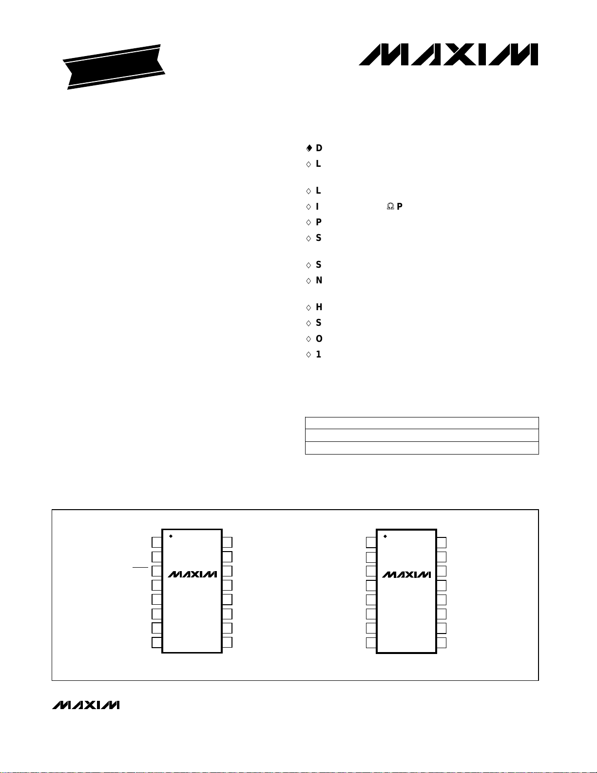
__________________________________________________________Pin Configurations
TOP VIEW
UP
1
DN
2
SHDN
3
SYNC
SS
CC
CSAV
MINDAC
________________________________________________________________
4
5
6
7
8
MAX1610
SO
16
BATT
LX
15
BST
14
GND
13
VL
12
11
CS
10
OTP
9
REF
SDA
SCL
SMBSUS
SYNC
CC
CSAV
MINDAC
1
2
3
MAX1611
4
SS
5
6
7
8
SO
16
BATT
15
LX
14
BST
GND
13
VL
12
11
CS
10
OTP
9
REF
Maxim Integrated Products
1
For free samples & the latest literature: http://www.maxim-ic.com, or phone 1-800-998-8800
Page 2
Digitally Controlled CCFL Backlight
Power Supplies
ABSOLUTE MAXIMUM RATINGS
BATT to GND............................................................-0.3V to 28V
BST to GND ..............................................................-0.3V to 30V
BST to LX....................................................................-0.3V to 6V
LX to GND................................................-0.6V to (BATT + 0.3V)
VL to GND...................................................................-0.3V to 6V
CS, CSAV, CC, SYNC, REF, MINDAC,
SS, OTP to GND............................................-0.3V to (VL + 0.3V)
SHDN, UP, DN to GND...............................................-0.3V to 6V
SMBSUS, SDA, SCL to GND ......................................-0.3V to 6V
Stresses beyond those listed under “Absolute Maximum Ratings” may cause permanent damage to the device. These are stress ratings only, and functional
operation of the device at these or any other conditions beyond those indicated in the operational sections of the specifications is not implied. Exposure to
absolute maximum rating conditions for extended periods may affect device reliability.
ELECTRICAL CHARACTERISTICS
(TA= 0°C to +70°C, BATT = 8.2V, MINDAC = 0V, unless otherwise noted. Typical values are at TA= +25°C.)
MAX1610/MAX1611
SUPPLY AND REFERENCE
BATT Input Voltage Range V
BATT Quiescent Supply Current,
Operate Mode
BATT = 25V
BATT, LX Current.....................................................................1A
SDA Current........................................................................50mA
VL Current...........................................................................50mA
Continuous Power Dissipation (T
SO (derate 8.70mW/°C above +70°C).........................696mW
Operating Temperature Range
MAX1610CSE/MAX1611CSE..............................0°C to +70°C
Storage Temperature Range.............................-65°C to +160°C
Lead Temperature (soldering, 10sec).............................+300°C
CONDITIONS
= +70°C)
A
MIN TYP MAXPARAMETER
4.75 26
UNITS
mA1.5 3
BATT Quiescent Supply Current,
Shutdown Mode
REF Load Regulation
SWITCHING REGULATOR
BATT-to-LX Switch On-Resistance
LX Switch Off-Leakage Current
Oscillator Frequency
SYNC Low Pulse Width
4.75V < BATT < 26V
No load
I
SOURCE
BST - LX = 4.1V
SYNC = REF
SYNC = GND
SYNC = GND or VL
SYNC = REF
SS = GND
SS = 0.5V mA2SS Sink Current
= 100µA
10 20
620
0.7 1.0
10
250 290 330
125 145 165
-1 1SYNC Input Current
2.5 4.0 5.5SS Source Current
µA
V4.25 4.5 4.75VL Output Voltage, Operate Mode
V3.0 3.6 4.75VL Output Voltage, Shutdown Mode
V1.92 2.0 2.08REF Output Voltage
mV
Ω
µA
kHz
kHz240 350Oscillator SYNC Pin Synchronization Range
ns200SYNC High Pulse Width
ns200
µA
V0.5SYNC Input Low Voltage
V4.0SYNC Input High Voltage
%89 91Power-Switch Maximum Duty Cycle
µA
2 _______________________________________________________________________________________
Page 3
Digitally Controlled CCFL Backlight
Power Supplies
ELECTRICAL CHARACTERISTICS (continued)
(TA= 0°C to +70°C, BATT = 8.2V, MINDAC = 0V, unless otherwise noted. Typical values are at TA= +25°C.)
CONDITIONS
DAC AND ERROR AMPLIFIER
DAC Resolution Bits5
CSAV Regulation Point
CSAV to CC Voltage-to-Current Converter
Transconductance
CC Sink Current
OPEN AND SHORTED TUBE PROTECTION
MAX1610 LOGIC LEVELS
SHDN, UP, DN Input Low Voltage
SHDN, UP, DN Input High Voltage
SHDN, UP, DN Input Bias Current
MAX1611 LOGIC LEVELS
Guaranteed monotonic
-1 1MINDAC Input Bias Current
D/A at full scale
D/A at 1LSB 12
CC = 2V, CSAV = 1V, D/A at 1LSB
CC = 2V, CSAV = 1V, D/A at 1LSB
CC = 2V, CSAV = 0V, D/A at full scale
Referred to REF
GND < OTP < VL
V
= 0.6V mA6SDA Output Low Sink Current
SDA
OTP rising
232 247 260
-5 5CSAV Input Bias Current
-1 1OTP Input Bias Current
-1 1
-1 1SMBSUS, SDA, SCL Input Bias Current
85
80
20CC Source Current
MAX1610/MAX1611
UNITSMIN TYP MAXPARAMETER
V01MINDAC Input Voltage Range
µA
V3MINDAC Digital PWM Threshold
V0 1.0CSAV Input Voltage Range
mV
µA
µmho
µA
µA
mV-20 20OTP Voltage Trip Point
µA
mV500CS Overcurrent Cutoff Threshold
V0.8
V2.4
µA
V0.8SMBSUS, SDA, SCL Input Low Voltage
V2.2SMBSUS, SDA, SCL Input High Voltage
µA
_______________________________________________________________________________________ 3
Page 4
Digitally Controlled CCFL Backlight
Power Supplies
TIMING CHARACTERISTICS—MAX1610
(Figure 1, TA= +25°C, unless otherwise noted.)
CONDITIONS
UP, DN Pulse Width High
UP, DN Pulse Width Low
UP, DN Pulse Separation
Counter Reset Time
TIMING CHARACTERISTICS—MAX1611
(Figures 2 and 3, TA= +25°C, unless otherwise noted.)
1
2
3
4
UNITSMIN TYP MAXSYMBOLPARAMETER
1t
1t
1t
1t
µs
µs
µs
µs
SCL Serial Clock High Period
SCL Serial Clock Low Period
MAX1610/MAX1611
SCL, SCA Rise Time
SCL, SDA Fall Time
Start Condition Setup Time
Start Condition Hold Time
SDA Valid to SCL Rising Edge
Setup Time, Slave Clocking in Data
SCL Falling Edge to SDA
Transition
SCL Falling Edge to SDA Valid,
Reading Out Data
Note 1: Guaranteed by design.
HIGH
LOW
R
F
SU:STA
HD:STA
SU:DAT
HD:DAT
DV
(Note 1)
(Note 1)
(Note 1) ns0t
CONDITIONS
UNITSMIN TYP MAXSYMBOLPARAMETER
4t
4.7t
1t
0.3t
4.7t
4t
500t
1t
µs
µs
µs
µs
µs
µs
ns
µs
4 _______________________________________________________________________________________
Page 5
Digitally Controlled CCFL Backlight
Power Supplies
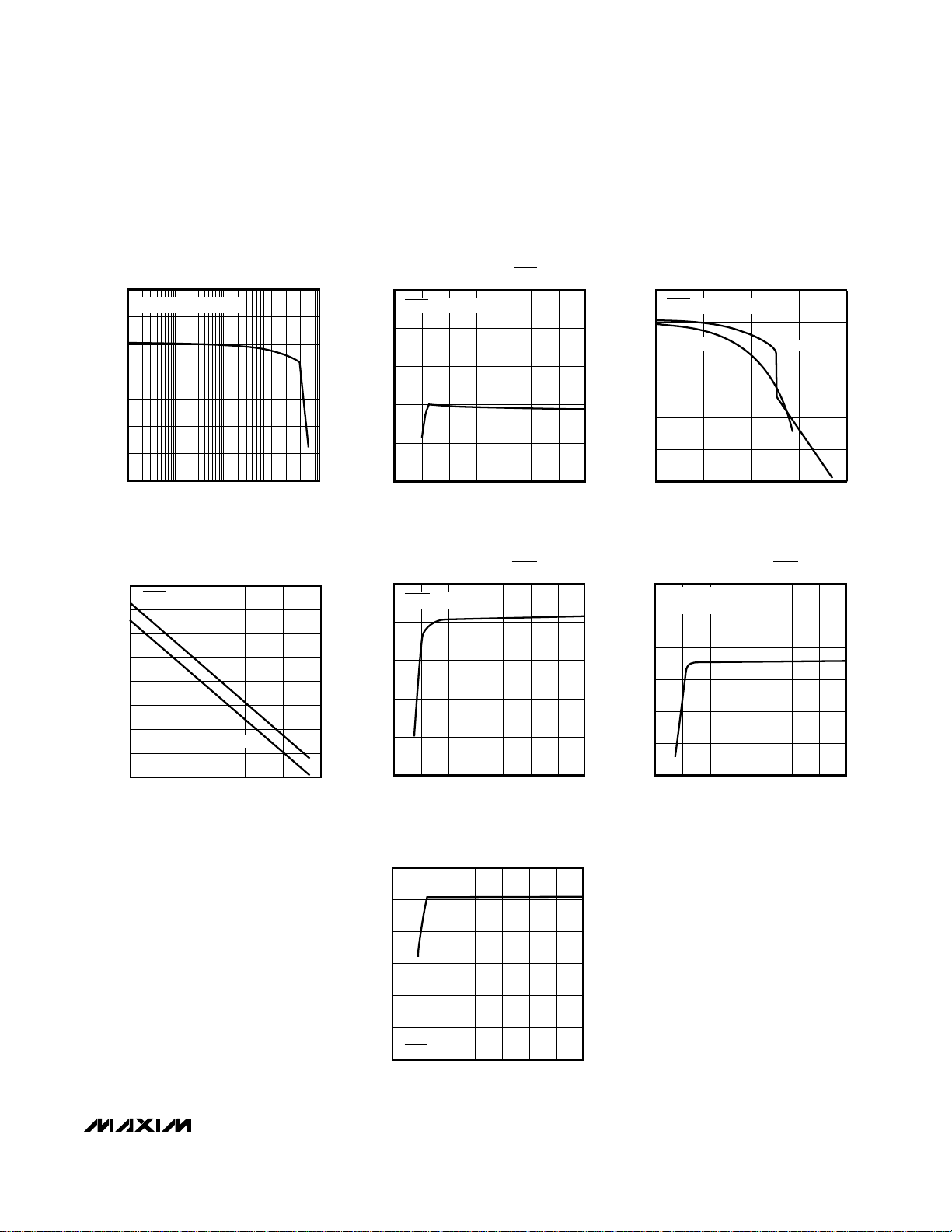
__________________________________________Typical Operating Characteristics
(TA = +25°C, unless otherwise noted.)
REF OUTPUT VOLTAGE
vs. REF OUTPUT CURRENT
2.2
SHDN = VL, BATT = 5V
2.1
2.0
1.9
1.8
1.7
REF OUTPUT VOLTAGE (V)
1.6
1.5
10 100 1000 10000
1
REF OUTPUT CURRENT (µA)
VL OUTPUT VOLTAGE
vs. VL LOAD CURRENT
3.70
SHDN = GND
3.65
3.60
3.55
3.50
3.45
VL VOLTAGE (V)
3.40
3.35
3.30
0
BATT = 12V
VL LOAD CURRENT (µA)
BATT = 5V
400 800600 1000200
MAX1610/1611-TOC1
BATT CURRENT (mA)
MAX1610/1611-TOC4
BATT CURRENT (µA)
2.0
1.8
1.6
1.4
1.2
1.0
10
8
6
4
2
0
BATT SUPPLY CURRENT
vs. BATT VOLTAGE (SHDN = VL)
SHDN = VL, OTP = 3V
4 12162024288
0
BATT (V)
BATT SUPPLY CURRENT
vs. BATT VOLTAGE (SHDN = OV)
SHDN = OV
4 12162024288
0
BATT (V)
MAX1610/1611-TOC2
VL VOLTAGE (V)
MAX1610/1611-TOC5
VL (V)
VL OUTPUT VOLTAGE
vs. VL OUTPUT CURRENT
5.0
SHDN = VL, OTP = 3V
4.5
BATT = 5V
4.0
3.5
3.0
2.5
2.0
0
VL OUTPUT CURRENT (mA)
VL OUTPUT VOLTAGE
vs. BATT VOLTAGE (SHDN = OV)
5.0
NO LOAD ON VL,
SHDN = OV
4.5
4.0
3.5
3.0
2.5
2.0
0
4 12162024288
BATT (V)
BATT = 12V
MAX1610/1611-TOC3
20 30 4010
MAX1610/1611-TOC6
MAX1610/MAX1611
VL OUTPUT VOLTAGE
vs. BATT VOLTAGE (SHDN = VL)
5.0
4.5
4.0
3.5
VL (V)
3.0
2.5
2.0
NO LOAD ON VL,
SHDN = VL
0
4 12162024288
BATT (V)
MAX1610/1611-TOC7
_______________________________________________________________________________________
5
Page 6
Digitally Controlled CCFL Backlight
Power Supplies
______________________________________________________________Pin Description
PIN
MAX1610 MAX1611
1 — UP
— 1 SDA
2 — DN
— 2 SCL
3 —
— 3 SMBSUS
MAX1610/MAX1611
4 4 SYNC
5 5 SS
6 6 CC
7 7 CSAV
8 8 MINDAC
9 9 REF
10 10 OTP
11 11 CS
12 12 VL
13 13 GND
14 14 BST
15 15 LX
16 16 BATT
NAME
SHDN
Logic-Level Input. A rising edge on UP increments the 5-bit counter for the 5-bit DAC.
UP = DN = 1 presets the counter to mid-scale.
System Management Bus Serial Data Input and Open-Drain Output
Logic-Level Input. A rising edge on DN decrements the 5-bit counter for the 5-bit DAC.
UP = DN = 1 presets the counter to mid-scale.
System Management Bus Serial Clock Input
Logic-Level Shutdown Input Pin. Applying a logic low to SHDN places the chip in a low-
supply-current shutdown mode.
System Management Bus Suspend Mode Input. SMBSUS Selects one of two chip-
configuration settings, which are preprogrammed serially.
Oscillator Synchronization Input. Tying SYNC to REF sets the oscillator frequency to 290kHz.
Tying SYNC to GND or VL lowers the oscillator frequency to 145kHz.
Soft-Start Pin. A 4µA current source feeds the capacitor placed on SS. The voltage on this
pin limits the peak current in the switch. When the lamp is turned off, SS pulls to GND.
Output of the Voltage-to-Current Converter; Input to the PWM Comparator, which sets the
current limit. A capacitor placed at CC sets the current-regulator-loop bandwidth.
Input to the Voltage-to-Current Converter, which averages the voltage on CSAV using the
capacitor on CC.
The voltage at MINDAC sets the DAC’s minimum-scale output voltage. Tying MINDAC to
VL enables the internal 280Hz current-chopping mode.
2.0V Reference Output. Bypass with 0.1µF to GND.
Open-Tube Protection Comparator. As long as OTP exceeds the reference voltage, the
N-channel BATT-to-LX switch is forced off.
Low-Side Current-Sense Input. The current-mode regulator terminates the switch cycle
when the voltage at CS exceeds REF - CC.
Output of the Internal Linear Regulator. VL can be overdriven by a voltage greater than 4.75V
to operate the chip from +5V ± 5%, and to conserve power. Bypass with 0.1µF to GND.
System Ground
Power Input to the High-Side Gate Driver, which switches the internal N-channel MOSFET
on and off.
Ground Connection for the Internal High-Side Gate Driver; source-connection point for the
internal N-channel MOSFET
4.5V to 25V Battery-Voltage Input Point. Connects to the internal N-channel power MOSFET’s
drain, and to the input of the internal linear regulator that powers the chip.
FUNCTION
6 _______________________________________________________________________________________
Page 7
Digitally Controlled CCFL Backlight
Power Supplies
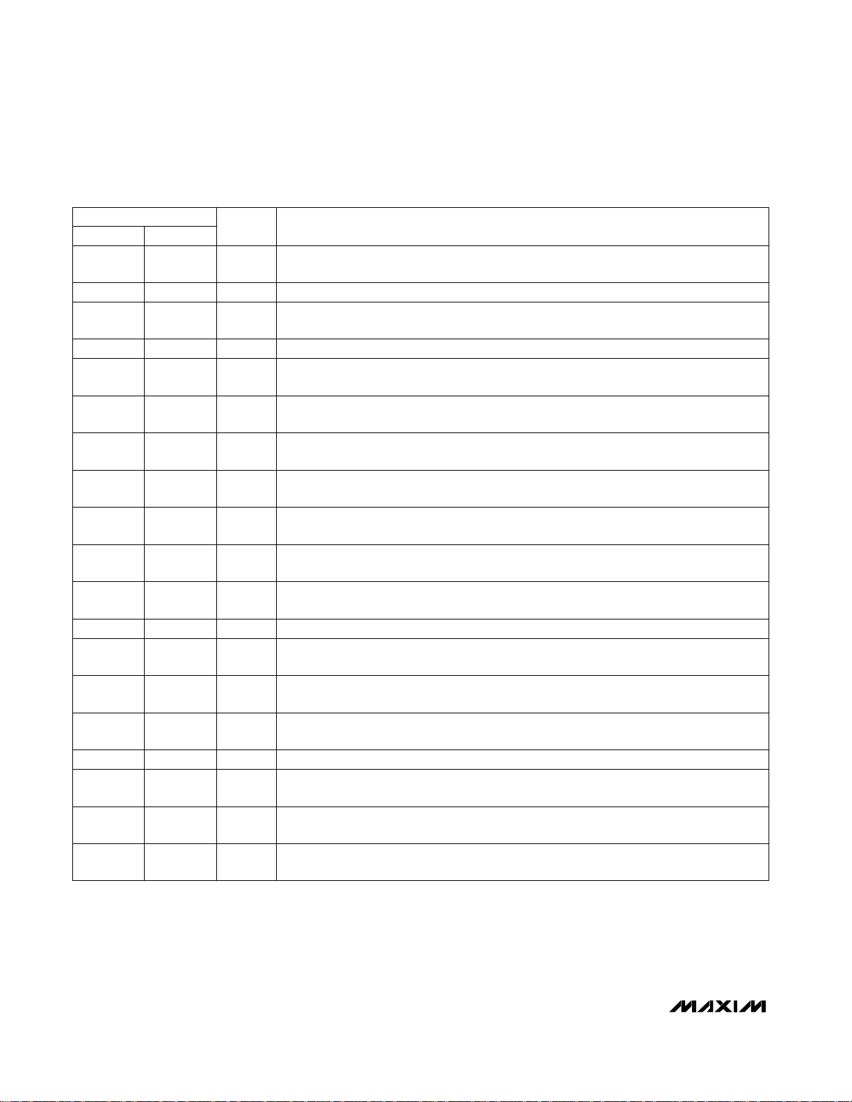
MAX1610/MAX1611
t
1
UP
DN
Figure 1. MAX1610 UP and DN Signal Timing
START
CONDITION
SCL
MOST SIGNIFICANT
ADDRESS BIT (A6)
CLOCKED INTO SLAVE
t
2
t
3
A5 CLOCKED
INTO SLAVE
A4 CLOCKED
INTO SLAVE
t
4
A3 CLOCKED
INTO SLAVE
• • •
t
HD:STA
SDA
t
SU:STA
t
SU:DAT
t
HD:DAT
Figure 2. MAX1611 SMB Serial-Interface Timing—Address
_______________________________________________________________________________________ 7
t
LOW
t
SU:DAT
t
HD:DAT
t
HIGH
• • •
Page 8

Digitally Controlled CCFL Backlight
Power Supplies
RW BIT
CLOCKED
INTO SLAVE
SCL
• • •
SDA
• • •
Figure 3. MAX1611 SMB Serial-Interface Timing—Acknowledge
MAX1610/MAX1611
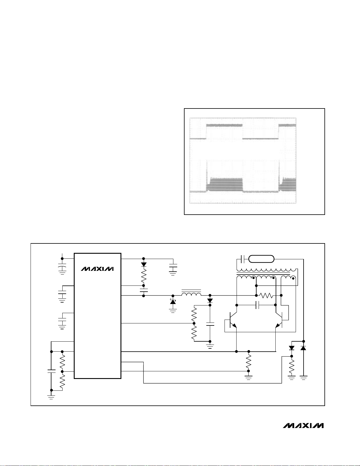
_______________Detailed Description
Getting Started
A cold-cathode fluorescent lamp (CCFL) has two terminals. For the CCFL to emit light, the two lamp terminals
must be driven with a high-voltage (approximately
550V AC RMS) and high-frequency (approximately
45kHz) sine wave. The MAX1610/MAX1611 use a varying DC input voltage to create this high-voltage, highfrequency sine-wave drive. To select the correct
component values for the MAX1610/MAX1611 circuit,
several CCFL parameters and the minimum DC input
voltage must be specified; these are listed in Table 1.
Table 3 shows the recommended component values to
use with the circuit of Figure 4, depending on the particular CCFL parameters. The C2 values in Table 3
have been selected such that the normal operating
voltage on the secondary of T1 is as close as possible
to the CCFL strike voltage (where the strike voltage
(VS) is assumed to be approximately 1.8 times the
CCFL operating voltage (VL)).
Components T1, C1, R2, Q1, and Q2 form a Royer
oscillator. A Royer oscillator is a resonant tank circuit
that oscillates at a frequency dependent on C1, the primary magnetizing inductance of T1 (LP), and the
impedance seen by the T1 secondary. The
MAX1610/MAX1611 regulate the current fed into the
Royer oscillator by sensing the voltage on R1. For a
given current through the Royer oscillator (IR1), the
power delivered to the CCFL depends on the Royer
oscillator frequency. The R1 values in Table 3 have
been selected to ensure that the power into the CCFL
ACKNOWLEDGED
BIT CLOCK
INTO MASTER
SLAVE PULLING
SDA LOW
t
DV
MOST SIGNIFICANT
BIT CLOCKED
t
DV
does not exceed its maximum rating, despite T1, C1, and
C2 component-value variations. The Royer oscillator
waveforms for the circuit of Figure 4 are shown in Figures
5 and 6.
Analog Circuitry
The MAX1610/MAX1611 maintain fixed CCFL brightness with varying input voltages on BATT by regulating
the current fed into the Royer oscillator. This current is
sensed via resistor R1 between CSAV and GND. An
internal switch from BATT-to-LX pulse-width modulates
at a fixed frequency to servo the CSAV pin to its regulation voltage. The CSAV regulation voltage can be
adjusted via the digital interface to set CCFL brightness. The MAX1610 and MAX1611 differ only in the
digital interface they use to adjust the internal 5-bit digital-to-analog converter (DAC) that sets the CSAV regulation voltage. The minimum-scale (min-scale) CSAV
regulation voltage is resistor adjustable using the MINDAC pin, setting the minimum CCFL brightness. The
D/A setting at MAX1610/MAX1611 power-up is preset
to mid-scale (10000 binary) (Figure 7).
MINDAC Sets the Minimum Scale
The MINDAC pin sets the lowest CCFL brightness
level. The voltage at MINDAC is divided by eight, and
sets the minimum CSAV regulation voltage. For example, in the circuit of Figure 4, R5 (150kΩ) and R6
(51kΩ) form a resistor divider from REF, which sets
MINDAC to 507mV (REF = 2.0V). This sets a minimum
CSAV regulation voltage of 63mV with a full-scale
CSAV regulation voltage of 247mV.
8 _______________________________________________________________________________________
Page 9

Digitally Controlled CCFL Backlight
Power Supplies
MAX1610/MAX1611
V
IN
16
BATT
+
C9
MAX1610
MAX1611*
5
SS
C4
6
CC
C3
4
SYNC
9
REF
R5
C8
8
MINDAC
R6
BST
OTP
CSAV
GND
12
VL
D3
14
15
LX
10
11
CS
7
13
R7
C7
C6
L1
D2
R3
R4
D1
C5
C2
CCFL
10
R2
C1
Q2Q1
R1
6
T1
53421
* DIGITAL INTERFACE NOT SHOWN
Figure 4. Typical Floating-Lamp Application Circuit
Table 1. Necessary CCFL Specifications
SYMBOL
V
S
V
L
I
L
f
L
V
MIN
CCFL Minimum Strike Voltage
(“Kick-Off Voltage”)
CCFL Typical Operating Voltage
(“Lamp Voltage”)
CCFL Maximum Operating
Current (“Lamp Current”)
(“Lamp Frequency”)
DC Power Source Minimum
Input Voltage
UNITS
V
RMS
V
RMS
mA
RMS
kHz
V
DESCRIPTIONSPECIFICATION
Although CCFLs typically operate at 550V
a higher voltage
RMS,
is required initially to light up the tube.
Once a CCFL has been struck, the voltage required to maintain
light output falls to approximately 550V
operate on as little as 250V
. The operating voltage of the
RMS
. Small tubes may
RMS
CCFL stays relatively constant, even as the tube’s brightness is
varied.
The maximum root-mean-square AC current through a CCFL is
almost always 5mA
No DC current is allowed through any
RMS.
CCFL.
The maximum AC-lamp-current frequency.CCFL Maximum Frequency
The minimum DC input voltage to the MAX1610/MAX1611 circuit
determines the turns ratio required for the DC-AC conversion
transformer. Decreasing the minimum input voltage increases
the size of the transformer required for a given output power.
_______________________________________________________________________________________ 9
Page 10

Digitally Controlled CCFL Backlight
Power Supplies
Table 2. Typical Application Circuit Component Values
a) Resistors
SYMBOL
R1 ±1% 1/8W
R2 ±10% 1/8W
R3 ±5% 1/16W
R4 ±5% 1/16W
R5 ±5% 1/16W
R6 ±5% 1/16W
R7 ±10% 1/16W
MAX1610/MAX1611
c) Other Components
SYMBOL
Q1, Q2 2N2222A FMMT619, SOT23
D1, D3 1N4148 CMPD4448, SOT23
VALUE
(Note)
510Ω
51kΩ
8.2kΩ
150kΩ
51kΩ
20Ω
D2 1N5818 EC10QS04
L1 CDR125-101
TOLERANCE
1A NPN switching transistor,
V
≥ 50V
CEO
50mA silicon diode, VBR≥ 40V
1A Schottky diode, VBR≥ 30V
100µH, 1A inductor
POWER
RATING
DESCRIPTION
b) Capacitors
SYMBOL
C1 ±20% ±25V
C2 ±10% ±3kV
C3, C5 ±20% 25V
C4, C6,
C7, C8
C9 -50% 35V
VALUE
0.1µF
(Note 1)
(pF)
27nF
0.1µF
10µF
GENERIC
PART
TOLER-
ANCE
-20% 25V
SURFACE-MOUNT
WORKING
VOLTAGE
PART
NOTES
δF ≤ 0.001 @ 1kHz
High voltage
Ceramic, larger
values acceptable
Tantalum, low ESR
MANUFACTURER
Zetex
Central
Nihon
Sumida
6W Royer oscillator transformer, turns ratio 67:1,
T1 CTX110605
Note: Component values depend on lamp characteristics. See Table 3 to select values.
secondary (pins 10 and 6) : primary (pins 1 and 3),
primary magnetizing inductance (LP) of 44µH ±20%
Table 3. Selecting Circuit Values for Figure 4
V
L
(V
)
RMS
250 3 50.3 58.6 71.8
250
300 3 52.1 61.0 75.1
300 5 45.6 52.8 64.7
450 5 51.1 59.7 73.3
500 5 52.1 61.0 75.1
550 5 52.5 61.8 76.7
600 5 53.6 63.1 78.1
Note: f
10 ______________________________________________________________________________________
= Royer oscillator damped resonant oscillation frequency. T1 primary magnetizing inductance (LP) = 44µH ±20%.
ROY
VCT = average voltage from the T1 center tap to the emitters of Q1 and Q2 (ignoring Q1, Q2 V
C1 = 0.1µF ± 20%; C2 = ±10% tolerance; R1 = ±1% tolerance.
I
L
(mA
)
RMS
5 43.3 49.7 60.3
C2
22pF
43pF
18pF
36pF
20pF
18pF
18pF
R1
1.21Ω
0.715Ω
1.18Ω
0.681Ω
0.732Ω
0.715Ω
0.665Ω
0.698Ω
VCT
(V
MAX
3.63V
3.61V
4.30V
4.14V
6.55V
7.17V
7.29V
8.41V15pF
)
MIN TYP MAX
).
CE,SAT
Coiltronics
f
(kHz)
ROY
Page 11
FIGURE 4 CIRCUIT, C2 = 15pF, I
CCFL VL = 500V
BATT = 10V, I
MINDAC = 0.5V, D/A VALUE = 11111
RMS
BATT
= 0.20A,
R1
Digitally Controlled CCFL Backlight
Power Supplies
= 462mA,
6V
T1
CENTER-TAP
VOLTAGE
0V
1A
C1
CURRENT
-1A
FIGURE 4 CIRCUIT, C2 = 15pF,
R1 = 545Ω,
CCFL VL = 500V
MINDAC = 0.5V, D/A VALUE = 10000
, BATT = 15V,
RMS
3V
SS
VOLTAGE
0V
6V
T1
CENTER-TAP
VOLTAGE
0V
MAX1610/MAX1611
5µs/div
Figure 5. Royer Oscillator Typical Operating Waveforms for
Circuit of Figure 4
REF / 8 = 250mV
FULL-SCALE
MID-SCALE
CSAV REGULATION VOLTAGE
10ms/div
Figure 6. Start-Up Waveforms for Circuit of Figure 4
MIN-SCALE = MINDAC / 8
OmV
NOTE: DAC CODE 00000 FORCES THE BATT-TO-LX SWITCH OFF REGARDLESS OF CSAV OR MINDAC VOLTAGE.
Figure 7. CSAV Regulation Voltage Range
______________________________________________________________________________________ 11
00001
00000
00010
00011
00100
00101
00110
00111
01000
01001
01010
01011
01100
01101
01110
10000
01111
DAC CODE
10001
10010
10011
10100
10101
10110
10111
11000
11001
11010
11011
11100
11101
11110
11111
Page 12

Digitally Controlled CCFL Backlight
Power Supplies
Open-Tube Protection (OTP)
Any real transformer used in a Royer oscillator will have a
maximum-allowed secondary voltage. If the maximumallowed secondary voltage is exceeded, the winding
insulation can break down, leading to permanent transformer damage. The maximum-allowed secondary voltage can be exceeded either when the CCFL drive circuit
is turned on without the CCFL being in place, or when
the CCFL becomes disconnected during normal operation due to a mechanical failure. To protect against these
fault conditions, use the OTP pin to sense the voltage on
the transformer center tap (pin 2 of Figure 4). Whenever
the voltage on OTP exceeds the REF reference voltage,
the BATT-to-LX power switch is forced off.
For example, in Figure 4, the CTX110605 transformer
has a maximum-allowed continuous secondary voltage
of 1340V
D1 and C5 detect the peak voltage on
RMS.
the center tap of T1. R3 and R4 determine the limit on
MAX1610/MAX1611
the center tap peak voltage. The relationship between
the voltage on the center tap of T1 and the secondary
voltage is diagrammed in Figure 8. Neglecting the
Q1/Q2 saturation voltage and the voltage on the R1
current-sense resistor yields Equation 1:
V2
SEC
2N
where V
V =
CTPK
is the maximum root-mean-square voltage
SEC
allowed on the secondary, N is the secondary-to-primary turns ratio, and V
is the peak voltage on the
CTPK
transformer center tap.
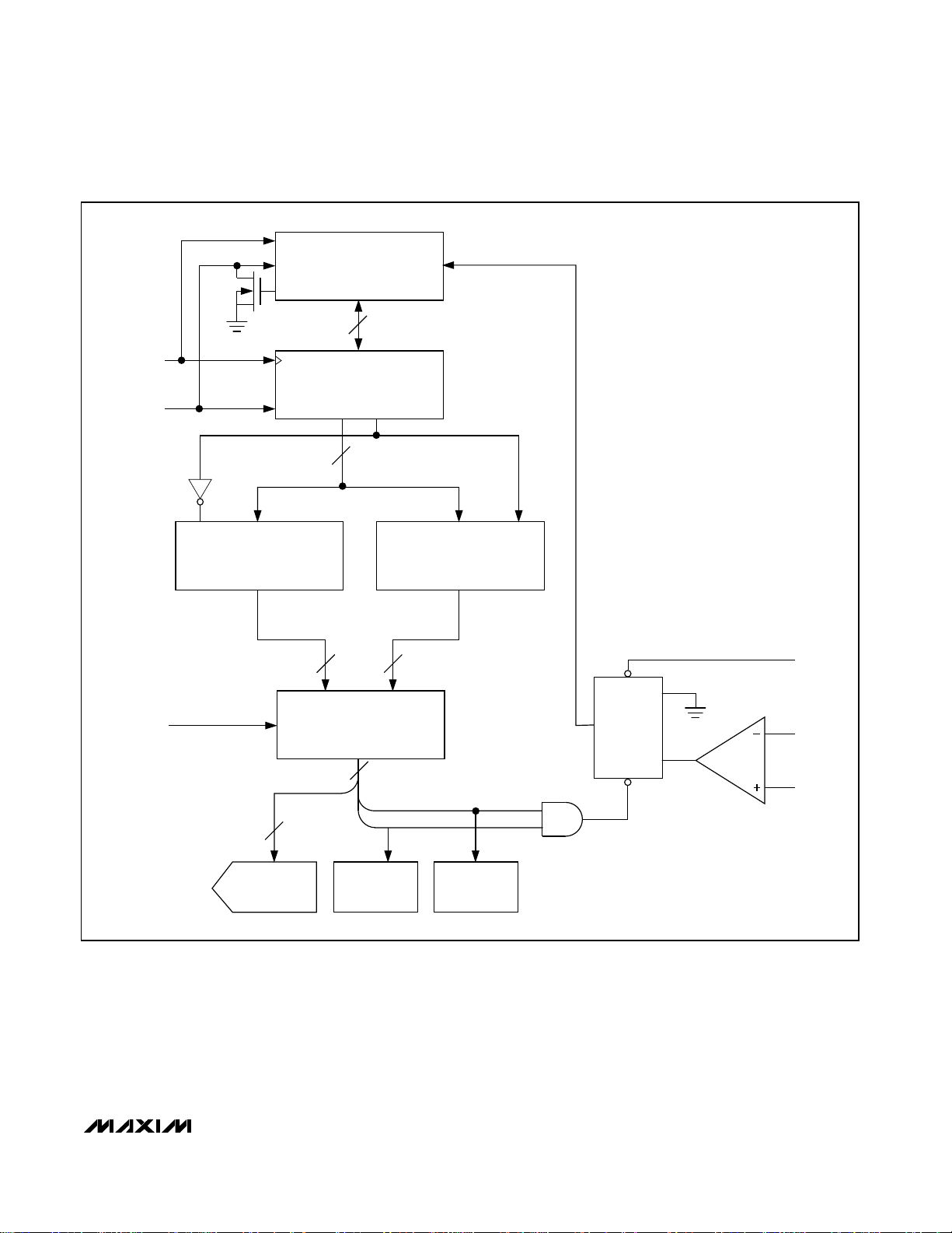
Block Diagram of the Analog Section
Figure 9 shows a functional diagram of the analog circuitry in the MAX1610/MAX1611. The chips have identical analog circuitry, and differ only in their digital
interface.
Loop-Compensation Capacitor (CC)
The BATT-to-LX switch turns on at fixed frequency, and
turns off when the current-sense voltage on the CS pin
exceeds CC - REF. As the CC pin voltage rises, the CS
current limit rises as well. A transconductance amplifier
compares the voltage on CSAV to the desired regulation
voltage and outputs a current proportional to this error
to the CC pin. A capacitor from CC to GND sets the
bandwidth of this regulation loop, as shown in Equation 2:
BW =
85
2C3
π
where BW is the bandwidth of the CSAV regulation loop
in kHz, and C3 is the capacitance from CC to GND
in nF.
Soft Start (SS)
Soft start prevents the triggering of OTP upon powerup. Placing a capacitor from SS to GND soft starts the
Royer oscillator by slowly raising the CS current-limit
voltage. Internal circuitry pulls SS to GND during
power-on reset, or whenever the lamp is turned off (DAC
= 00000, shutdown mode, ON-1 = 0, or ON-0 = 0)
(Figures 10 and 11). When SS is not pulled to GND, an
internal 4µA current sources into the capacitor at the
SS pin. This pin is internally diode clamped to REF so
that it rises to a maximum voltage of about 2.7V.
Regardless of the voltage on CC, the CS current-sense
voltage is never allowed to exceed the voltage on SS
divided by 5.
Frequency Selection and Synchronization
The SYNC pin performs two functions: it sets the BATTto-LX switching frequency, and it allows the BATT-to-LX
switching frequency to be synchronized to an external
oscillator. SYNC tied to GND or VL sets a 145kHz
switching frequency; SYNC tied to REF sets a 290kHz
πVCT
2
VOLTAGE (PIN 2)
T1 PRIMARY CENTER-TAP
NOTE: VCT = AVERAGE VOLTAGE FROM THE T1 CENTER TO THE EMITTERS OF Q1 AND Q2 (IGNORING Q1, Q2 V
Figure 8. Transformer Primary/Secondary Voltage Relationship
12 ______________________________________________________________________________________
2π
ω
NπVCT
2
T1 SECONDARY
-NπVCT
2
VOLTAGE (PIN 10–PIN 6)
2π
ω
). ω = 2πf
CE, SAT
ROY
.
Page 13

BATT
BST
CSAV
Digitally Controlled CCFL Backlight
Power Supplies
VL
GND
LX
CS
DMOS
POWER
SWITCH
LEVEL
SHIFTER
4.5V
REG
Σ
MAX1610/MAX1611
REF
MINDAC
SYNC
OTP
CC
SS
GM
(NOTE)
OSC
UP (SDA)
DN (SCL)
SHDN (SMBSUS)
÷8
+
2.0V
-
5-BIT DAC
5
DIGITAL INTERFACE
4µA
R
S
Q
÷5
( ) ARE FOR MAX1611
NOTE: CIRCUITRY TO DETECT MINDAC = VL NOT SHOWN. SEE
Figure 9. Functional Diagram
______________________________________________________________________________________ 13
CHOPPING THE LAMP CURRENT
SECTION.
Page 14

Digitally Controlled CCFL Backlight
Power Supplies
SIGNIFICANT
ADDRESS BIT
START
CONDITION
SCL
SDA
MOST
LEAST
SIGNIFICANT
ADDRESS BIT
R/W BIT
SLAVE
ACKNOWLEDGE
MOST
SIGNIFICANT
DATA BIT
REGSEL
SLAVE PULLS
SDA LOW
Figure 10. MAX1611 Serial-Interface Single-Byte Write Example (REGSEL = 0)
MOST
MAX1610/MAX1611
SIGNIFICANT
ADDRESS BIT
START
CONDITION
SCL
SDA
LEAST
SIGNIFICANT
ADDRESS BIT
R/W BIT
SLAVE
ACKNOWLEDGE
MOST
SIGNIFICANT
DATA BIT
REGSEL
SLAVE PULLS
SDA LOW
SHDNB-0
SHDNB-1
STDBY-0
STDBY-1
D4-0
D3-0 D2-0 D1-0 D0-0
D4-1
D3-1 D2-1 D1-1 D0-1
SLAVE
ACKNOWLEDGE
LEAST
SIGNIFICANT
DATA BIT
SLAVE PULLS
SDA LOW
SLAVE
ACKNOWLEDGE
LEAST
SIGNIFICANT
DATA BIT
SLAVE PULLS
SDA LOW
Figure 11. MAX1611 Serial-Interface Single-Byte Write Example (REGSEL = 1)
switching frequency. Any rising edge on SYNC restarts
a BATT-to-LX switch cycle by forcing the switch on.
________MAX1610 Digital Interface
The MAX1610 contains an internal 5-bit up/down counter
that sets the value of the internal 5-bit DAC. At power-on,
or when both the UP and DN pins are held high simultaneously, the 5-bit up/down counter is preset to 10000
binary, which corresponds to mid-scale. A rising edge
on UP increments the 5-bit up/down counter. A rising
edge on DN decrements the 5-bit up/down counter. The
counter will not roll over on either underflow or overflow.
For example, if the CCFL is at maximum intensity level,
rising edges on UP will not change the output.
The SHDN pin provides a way to lower the MAX1610
supply current to 10µA without resetting the 5-bit
up/down counter. With SHDN = 1, the MAX1610 operates normally with VL at 4.5V. When the BATT-to-LX
power switch operates, an additional 3mA of current
14 ______________________________________________________________________________________
(other than the supply current) is consumed through
the BST pin, requiring VL to source at least 4.5mA of
current. With SHDN = 0, all analog circuitry turns off,
except for a coarse regulator that can source up to
500µA from VL. The coarse regulator preserves the
state of the internal logic and keeps the digital interface
active during shutdown (SHDN = 0).
________MAX1611 Digital Interface
A single byte of data written over the Intel System
Management Bus (SMBus™) controls the MAX1611.
Figures 10 and 11 show example single-byte writes. The
MAX1611 contains two 7-bit latches for storing configuration data. Only one of the 7-bit latches is active at a
time. The MAX1611 responds only to its own address,
0101101 binary. The SMBSUS pin selects which of the
two sets of configuration data is used. Figure 12 shows
a schematic diagram of the MAX1611’s digital circuitry.
Notice that the SMBSUS pin selects which one of the
Page 15
Digitally Controlled CCFL Backlight
Power Supplies
MAX1610/MAX1611
SCL
SHIFT REGISTER
SDA IN DATA LE
LE
7-BIT LATCH-0
A
SMBSUS
MULTIPLEXER
S
Y = A WHEN S IS LOW
D_
5
CONTROL
LOGIC
8-BIT
7
7
Y
OTPOK
8
LE
7-BIT LATCH-1
7
B
7
SHDNB
STDBY
VL
CLR
S
OTPOK
Q
R
PRE
OTP
COMPARATOR
REF
OTP
5-BIT DAC
SS
CIRCUITRY
Figure 12. MAX1611 Serial-Interface Circuitry Block Diagram
______________________________________________________________________________________ 15
BIAS
GENERATORS
Page 16
Digitally Controlled CCFL Backlight
Power Supplies
Table 4. MAX1611 Configuration Byte with REGSEL = 0
BIT
7 REGSEL
6 SHDNB-0
5 STDBY-0
4
MAX1610/MAX1611
3
2
1
0
* Initial register state after power-up.
NAME DESCRIPTION
D4-0
D3-0
D2-0
D1-0
D0-0
POR
STATE*
—
0
0
1
0
0
0
0
Register Select. A zero in this bit writes the remaining seven bits into the 7-bit latch-0
(Figure 13).
Complete Shutdown. Pulling SMBSUS low with SHDNB-0 = 0 places the MAX1611 into a
low-quiescent-current shutdown mode, with the reference off and the VL linear-regulator
output switched to a low-current, coarse regulation mode. Pulling SMBSUS low with
SHDNB-0 = 1 puts the MAX1611 into its normal operational mode, with the reference and
internal VL linear regulator fully on. SHDNB-0 supersedes STDBY-0. As long as SHDNB-0 = 0
and SMBSUS = 0, it doesn't matter what STDBY-0 is; the MAX1611 still shuts down.
Standby, disables CCFL supply only. As long as SMBSUS stays low and STDBY-0 = 0, the
internal power switch is kept off and SS is held shorted to GND; neither the internal reference nor the linear regulator is affected. With STDBY = 1 and SMBSUS low, the MAX1611
operates normally.
DAC Input Data. With the SMBSUS pin low, bits D4-0 through D0-0 set the DAC.
Table 5. MAX1611 Configuration Byte with REGSEL = 1
BIT
7 REGSEL
6 SHDNB-1
5 STDBY-1
4
3
2
1
0
NAME DESCRIPTION
D4-1
D3-1
D2-1
D1-1
D0-1
POR
STATE*
—
1
1
1
0
0
0
0
Register Select. A one in this bit writes the remaining seven bits into the 7-bit latch-1
(Figure 13).
Complete Shutdown. Pulling SMBSUS high with SHDNB-1 = 0 places the MAX1611 into a
low-quiescent-current shutdown mode, with the reference off and the VL linear regulator
output switched to a low-current coarse regulation mode. Pulling SMBSUS high with
SHDNB-1 = 1 puts the MAX1611 into its normal operational mode, with the reference and
internal VL linear regulator fully on. SHDNB-1 supersedes STDBY-1. As long as SHDNB-1 = 0
and SMBSUS = 0, it doesn’t matter what STDBY-1 is; the MAX1611 still shuts down.
Standby, disables CCFL supply only. As long as SMBSUS stays high and STDBY-1 = 0,
the internal power switch is kept off and SS is held shorted to GND; neither the internal reference nor the linear regulator is affected. With STDBY-1 = 1 and SMBSUS high, the
MAX1611 operates normally.
DAC Input Data. With the SMBSUS pin high, bits D4-1 through D0-1 set the DAC.
* Initial register state after power-up.
16 ______________________________________________________________________________________
Page 17

SIGNIFICANT
ADDRESS BIT
START
CONDITION
SCL
MOST
Digitally Controlled CCFL Backlight
Power Supplies
LEAST
SIGNIFICANT
ADDRESS BIT
R/W BIT
SLAVE
ACKNOWLEDGE
MOST
SIGNIFICANT
DATA BIT
MAX1610/MAX1611
SDA
Figure 13. MAX1611 Serial-Interface Read Example
Table 6. MAX1611 Status Bits
BIT
7 OTPOK
6
5
4
3
2
1
0
* Initial register state after power-up.
NAME FUNCTION
—
—
DA4
DA3
DA2
DA1
DA0
two 7-bit registers is used. Tables 4 and 5 describe the
data format for the configuration data.
Status information can be read from the MAX1611
using the SMBus read-byte protocol. Figure 13 shows
an example status read. Table 6 describes the status
information data format.
During shutdown (SMBSUS = 0 and SHDNB-0 = 0, or
SMBSUS = 1 and SHDNB-1 = 0), the MAX1611 serial
interface remains fully functional and can be used to set
either the SHDNB-0 or SHDNB-1 bits in order to return
the MAX1611 to its normal operational state.
POR
STATE*
1
—
—
Latched Open-Tube Detection. OTPOK = 0 indicates that open-tube detection has been
triggered. As soon as the voltage on the OTP pin exceeds REF, the OTPOK bit is cleared.
Reset the OTPOK pin by entering shutdown or standby.
Unused. These bits always return a logic one.
Displays the DAC setting selected by SMBSUS.
_______ Chopping the Lamp Current
Chopping the lamp current allows lower sustainable light
levels without lamp flicker. Intensity is varied by controlling the on-time duty cycle. Tying MINDAC to VL activates a special mode, which allows the CCFL intensity to
OTPOK
SLAVE PULLS
SDA LOW
DA4 DA3 DA2 DA1 DA0
MAX1611 DRIVES SDA
be varied by turning the lamp on and off at a frequency
faster than the eye can detect. The SS pin pulls to GND
during off time and rises to 2.7V during on time. During
on time, the CSAV pin regulates to REF / 8 (250mV).
During off time, the BATT-to-LX power switch is forced
off and the CC compensation node goes high impedance. Omit R5, R6, and C4 of the circuit in Figure 4.
In this mode, leave SS floating and increase the CC
capacitance to 0.1µF. Also, insert a 330Ω resistor in series
with D1 (Figure 4) to prevent the open-lamp detection circuit from being tripped by the repeated striking of the
lamp. The SS pin will oscillate at the switching frequency
divided by 1024 (283Hz with SYNC = REF). The intensity
can be varied with the duty cycle at the SS pin. The duty
cycle is set by the DAC in 3% increments. Duty cycle will
vary with intensity. Full-scale yields a 100% duty cycle.
DAC codes 00001, 00010, and 00011 all yield the
______________________________________________________________________________________ 17
Page 18
Digitally Controlled CCFL Backlight
Power Supplies
minimum 9% duty cycle. DAC code 00000 shuts off the
lamp entirely (0% duty cycle). Figure 14 shows the
chopped waveforms with the DAC set to mid-scale.
__________ Applications Information
Directly Regulating the Lamp Current
The MAX1610/MAX1611 can directly regulate the CCFL
current by tapping into the secondary of T1 (Figure 15).
This allows more precise setting of the maximum lamp
current (IL). The disadvantage of this approach is that
the secondary-to-ground voltage is twice that shown in
Figure 4, increasing the likelihood of the thermometer
effect, where one end of the lamp is brighter than the
other. Figure 15 uses the same component values as
Figure 4, except for R1, R40, D40, and D41. D40 and
D41 are the same type of diode as D1. R1 should be
0.68Ω ±10% to set a peak current limit of about 735mA.
Use a 107Ω ±1% resistor for R40 to set a lamp current
MAX1610/MAX1611
of 5mA
types without component adjustments.
Table 7 lists three different sources for C1. C1 requires
a low dissipation factor to prevent overheating as energy
is cycled between C1 and the T1 magnetizing induc-
. This circuit accepts a wide range of lamp
RMS
Component Suppliers
tance in the Royer resonant tank. Table 8 lists suppliers
for the high-voltage ballast capacitor, C2.
4V
SS
VOLTAGE
0V
BATT = 15V, MINDAC = VL, SS = OPEN, CC = 0.1µF,
C2 = 15pF, MID-SCALE SETTING, D/A VALUE = 10000
15V
T1
CENTER-TAP
VOLTAGE
0V
500µs/div
Figure 14. Chopped Waveforms
VIN
16
BATT
+
C9
12
VL
MAX1610
SS
CC
SYNC
REF
MINDAC
MAX1611
BST
OTP
CSAV
GND
14
15
LX
10
11
CS
7
13
5
C4
6
C3
4
9
R5
C8
8
R6
Figure 15. Directly Regulating the CCFL Current
C2
CCFL
D3
R7
C7
C6
L1
D2
R3
R4
D1
C5
10
T1
1
2
R2
C1
Q2Q1
R1
D40
6
534
D41
R40
18 ______________________________________________________________________________________
Page 19

Digitally Controlled CCFL Backlight
Power Supplies
Table 7. Capacitor C1 Supplier Information
LOCATION
914-347-2474
(0621) 8785-0
5-70-11-51
206-883-9200
CHEV0025J104
Elmsford, NY
WIMASMD7.3104 (0621) 8710457158
PACCOM
Electronics
Germany
Hong Kong
Redmond, WA
Valencia, CA 805-295-5920
Table 8. Capacitor C2 Supplier Information
AVX/Kyocera1808HA330KATMA
MurataGHM1040SL330J3K
PHONE
914-347-7230
58-06-84-74
206-881-6959
805-295-5928NOVACAP4040N104M250
LOCATION
Olean, NY
Vancouver, WA
Germany
Hong Kong
Smyrna, GA 404-436-3030404-436-1300
Germany 49-911-668719349-911-66870
Taiwan 886-2-536-6721886-2-562-4218
Old Bridge, NJ 908-679-3222908-679-3366Metuchen Capacitors, Inc.302C1812A330K
Sylmar, CA 818-364-6100818-364-9800Johanson Dielectrics302R29N330K
MAX1610/MAX1611
NOTES/CONTACTFAXSUPPLIERPART
Dissipation factor (tan δ)
at 1kHz and 20°C ≤ 0.008.
Dissipation factor (tan δ)
at 1kHz ≤ 0.002.
Dissipation factor (tan δ)
at 1kHz and 20°C ≤ 0.0015.
FAXPHONESUPPLIERPART
716-372-6316716-372-6611
206-695-5836206-696-2840
08131 9004-4408131 9004-0
852-765-8185852-363-3303
___________________Chip Information
TRANSISTOR COUNT : 5457
______________________________________________________________________________________ 19
Page 20

Digitally Controlled CCFL Backlight
Power Supplies
________________________________________________________Package Information
D
A
0.101mm
e
A1
B
MAX1610/MAX1611
0.004in.
HE
C
L
Narrow SO
SMALL-OUTLINE
PACKAGE
(0.150 in.)
0°-8°
DIM
A
A1
B
C
E
e
H
L
DIM
D
D
D
INCHES MILLIMETERS
MIN
0.053
0.004
0.014
0.007
0.150
0.228
0.016
PINS
8
14
16
MAX
0.069
0.010
0.019
0.010
0.157
0.244
0.050
INCHES MILLIMETERS
MIN
MAX
0.189
0.197
0.337
0.344
0.386
0.394
MIN
1.35
0.10
0.35
0.19
3.80
5.80
0.40
MIN
4.80
8.55
9.80
1.270.050
MAX
1.75
0.25
0.49
0.25
4.00
6.20
1.27
MAX
5.00
8.75
10.00
21-0041A
Maxim cannot assume responsibility for use of any circuitry other than circuitry entirely embodied in a Maxim product. No circuit patent licenses are
Maxim cannot assume responsibility for use of any circuitry other than circuitry entirely embodied in a Maxim product. No circuit patent licenses are
Maxim cannot assume responsibility for use of any circuitry other than circuitry entirely embodied in a Maxim product. No circuit patent licenses are
implied. Maxim reserves the right to change the circuitry and specifications without notice at any time.
implied. Maxim reserves the right to change the circuitry and specifications without notice at any time.
implied. Maxim reserves the right to change the circuitry and specifications without notice at any time.
20
__________________Maxim Integrated Products, 120 San Gabriel Drive, Sunnyvale, CA 94086 (408) 737-7600
20
__________________Maxim Integrated Products, 120 San Gabriel Drive, Sunnyvale, CA 94086 (408) 737-7600
20
__________________Maxim Integrated Products, 120 San Gabriel Drive, Sunnyvale, CA 94086 (408) 737-7600
© 1996 Maxim Integrated Products Printed USA is a registered trademark of Maxim Integrated Products.
© 1996 Maxim Integrated Products Printed USA is a registered trademark of Maxim Integrated Products.
© 1996 Maxim Integrated Products Printed USA is a registered trademark of Maxim Integrated Products.
 Loading...