

Page 1

19-5003; Rev 0; 10/09
12-Channel/8-Channel, Flash-Configurable System
Monitors with Nonvolatile Fault Registers
General Description
The MAX16070/MAX16071 flash-configurable system monitors supervise multiple system voltages. The
MAX16070/MAX16071 can also accurately monitor
(Q2.5%) one current channel using a dedicated highside current-sense amplifier. The MAX16070 monitors
up to twelve system voltages simultaneously, and the
MAX16071 monitors up to eight supply voltages. These
devices integrate a selectable differential or single-ended analog-to-digital converter (ADC). Device configuration information, including overvoltage and undervoltage
limits and timing settings are stored in nonvolatile flash
memory. During a fault condition, fault flags and channel
voltages can be automatically stored in the nonvolatile
flash memory for later read-back.
The internal 1% accurate 10-bit ADC measures each
input and compares the result to one overvoltage, one
undervoltage, and one early warning limit that can be
configured as either undervoltage or overvoltage. A fault
signal asserts when a monitored voltage falls outside the
set limits. Up to three independent fault output signals
are configurable to assert under various fault conditions.
Because the MAX16070/MAX16071 support a powersupply voltage of up to 14V, they can be powered
directly from the 12V intermediate bus in many systems.
The MAX16070/MAX16071 include eight/six programmable general-purpose inputs/outputs (GPIOs). GPIOs
are flash configurable as dedicated fault outputs, as a
watchdog input or output, or as a manual reset.
The MAX16070/MAX16071 feature nonvolatile fault memory for recording information during system shutdown
events. The fault logger records a failure in the internal
flash and sets a lock bit protecting the stored fault data
from accidental erasure. An SMBus™ or a JTAG serial
interface configures the MAX16070/MAX16071. The
MAX16070/MAX16071 are available in a 40-pin, 6mm x
6mm, TQFN package. Both devices are fully specified
from -40NC to +85NC.
Features
S Operate from 2.8V to 14V
S ±2.5% Current-Monitoring Accuracy
S 1% Accurate 10-Bit ADC Monitors 12/8 Voltage
Inputs
S Single-Ended or Differential ADC for System
Voltage/Current Monitoring
S Integrated High-Side, Current-Sense Amplifier
S 12/8 Monitored Inputs with Overvoltage/
Undervoltage/Early Warning Limit
S Nonvolatile Fault Event Logger
S Two Programmable Fault Outputs and One Reset
Output
S Eight General-Purpose Inputs/Outputs
Configurable as:
Dedicated Fault Outputs
Watchdog Timer Function
Manual Reset
Margin Enable
S SMBus (with Timeout) or JTAG Interface
S Flash Configurable Time Delays and Thresholds
S -40NC to +85NC Operating Temperature Range
Ordering Information
PART TEMP RANGE PIN-PACKAGE
MAX16070ETL+
MAX16071ETL+
+Denotes a lead(Pb)-free/RoHS-compliant package.
*EP = Exposed pad.
-40NC to +85NC
-40NC to +85NC
40 TQFN-EP*
40 TQFN-EP*
MAX16070/MAX16071
Applications
Networking Equipment
Telecom Equipment (Base Stations, Access)
Storage/Raid Systems
Servers
Pin Configuration and Typical Operating Circuits appear at
end of data sheet.
SMBus is a trademark of Intel Corp.
_______________________________________________________________ Maxim Integrated Products 1
For pricing, delivery, and ordering information, please contact Maxim Direct at 1-888-629-4642,
or visit Maxim’s website at www.maxim-ic.com.
Page 2

12-Channel/8-Channel, Flash-Configurable System
Managers with Nonvolatile Fault Registers
ABSOLUTE MAXIMUM RATINGS
VCC, CSP, CSM to GND ........................................-0.3V to +15V
CSP to CSM .......................................................... -0.7V to +0.7V
MON_, GPIO_, SCL, SDA, A0, RESET to GND
(programmed as open-drain outputs) .................-0.3V to +6V
EN, TCK, TMS, TDI to GND ....................................-0.3V to +4V
DBP, ABP to GND ...-0.3V to the lower of +3V and (VCC + 0.3V)
TDO, GPIO_, RESET
(programmed as push-pull outputs) .... -0.3V to (V
Stresses beyond those listed under “Absolute Maximum Ratings” may cause permanent damage to the device. These are stress ratings only, and functional
operation of the device at these or any other conditions beyond those indicated in the operational sections of the specifications is not implied. Exposure to absolute
maximum rating conditions for extended periods may affect device reliability.
DBP
+ 0.3V)
ELECTRICAL CHARACTERISTICS
(VCC = 2.8V to 14V, TA = -40NC to +85NC, unless otherwise specified. Typical values are at ABP = DBP = VCC = 3.3V, TA = +25NC.)
(Note 1)
PARAMETER SYMBOL CONDITIONS MIN TYP MAX UNITS
MAX16070/MAX16071
Operating Voltage Range V
Undervoltage Lockout (Rising) V
Undervoltage Lockout Hysteresis V
Minimum Flash Operating
Voltage
Supply Current I
ABP Regulator Voltage V
DBP Regulator Voltage V
Boot Time t
Flash Writing Time 8-byte word 122 ms
Internal Timing Accuracy (Note 3) -8 +8 %
EN Input Voltage
EN Input Current I
Input Voltage Range 0 5.5 V
CC
UVLO
UVLO_HYS
V
flash
CC
ABP
DBP
BOOT
V
TH_EN_R
V
TH_EN_F
EN
Reset output asserted low 1.2
(Note 2) 2.8 14
Minimum voltage on VCC to ensure the
device is flash configurable
Minimum voltage on VCC to ensure flash
erase and write operations
No load on output pins 4.5 7
During flash writing cycle 10 14
C
= 1μF, no load, VCC = 5V 2.85 3 3.15 V
ABP
C
= 1μF, no load, VCC = 5V 2.8 3 3.1 V
ABP
VCC > V
EN voltage rising 1.41
EN voltage falling 1.365 1.39 1.415
UVLO
Input/Output Current .........................................................20mA
Continuous Power Dissipation (TA = +70NC)
40-Pin TQFN (derate 26.3mW/NC above +70NC) .......2105mW
Operating Temperature Range .......................... -40NC to +85NC
Junction Temperature ....................................................+150NC
Storage Temperature Range ............................ -65NC to +150NC
Lead Temperature (soldering, 10s) ................................+300NC
V
2.7 V
100 mV
2.7 V
mA
200 350 μs
V
-0.5 +0.5 μA
2 ______________________________________________________________________________________
Page 3
12-Channel/8-Channel, Flash-Configurable System
Managers with Nonvolatile Fault Registers
ELECTRICAL CHARACTERISTICS (continued)
(VCC = 2.8V to 14V, TA = -40NC to +85NC, unless otherwise specified. Typical values are at ABP = DBP = VCC = 3.3V, TA = +25NC.)
(Note 1)
PARAMETER SYMBOL CONDITIONS MIN TYP MAX UNITS
ADC DC ACCURACY
Resolution 10 Bits
Gain Error ADC
Offset Error ADC
Integral Nonlinearity ADC
Differential Nonlinearity ADC
ADC Total Monitoring Cycle Time t
ADC IN_ Ranges
CURRENT SENSE
CSP Input-Voltage Range V
Input Bias Current
CSP Total Unadjusted Error CSP
Overcurrent Differential
Threshold
V
Fault Threshold
SENSE
Hysteresis
Secondary Overcurrent Threshold
Timeout
V
Ranges
SENSE
ADC Current Measurement
Accuracy
Gain Accuracy
Common-Mode Rejection Ratio CMRR
Power-Supply Rejection Ratio PSRR
CYCLE
I
I
CSM
OVC
OVC
OVC
CSP
CSP
GAIN
TA = +25°C 0.35
TA = -40°C to +85°C 0.70
OFF
INL
DNL
No MON_ fault detected 40 50 μs
1 LSB = 5.43mV 5.56
1 LSB = 1.36mV 1.39
3 14 V
14 25
V
= V
CSP
(Note 4) 2 %FSR
ERR
V
TH
HYS
DEL
SNSVCSP
SNS
CSP
V
CSM
r73h[6:5] = ‘00’ 0
r73h[6:5] = ‘01’ 3 4 5
r73h[6:5] = ‘10’ 12 16 20
r73h[6:5] = ‘11’ 50 64 60
Gain = 6 232
Gain = 12 116
Gain = 24 58
Gain = 48 29
V
SENSE
V
SENSE
V
SENSE
V
SENSE
V
SENSE
gain = 6
CSM
Gain = 48 21.5 25 30.5
Gain = 24 46 51 56
Gain = 12 94 101 108
Gain = 6 190 202 210
= 150mV (gain = 6 only) -2.5
= 50mV, gain = 12 -4
= 25mV, gain = 24
= 10mV, gain = 48
= 20mV to 100mV, V
> 4V 80 dB
CSP
= 5V,
-1.5 +1.5 %
3 5
0.5 % OVC
Q0.2
Q0.2
Q0.5
Q1
80 dB
1 LSB
1 LSB
1 LSB
+2.5
+4
%
V1 LSB = 2.72mV 2.78
μA
mV
TH
ms
mV
%
MAX16070/MAX16071
_______________________________________________________________________________________ 3
Page 4

12-Channel/8-Channel, Flash-Configurable System
Managers with Nonvolatile Fault Registers
ELECTRICAL CHARACTERISTICS (continued)
(VCC = 2.8V to 14V, TA = -40NC to +85NC, unless otherwise specified. Typical values are at ABP = DBP = VCC = 3.3V, TA = +25NC.)
(Note 1)
PARAMETER SYMBOL CONDITIONS MIN TYP MAX UNITS
OUTPUTS (RESET, GPIO_)
I
= 2mA 0.4
SINK
I
Output-Voltage Low V
Maximum Output Sink Current
Output-Voltage High (Push-Pull) I
Output Leakage (Open Drain) 1 μA
SMBus INTERFACE
Logic-Input Low Voltage V
Logic-Input High Voltage V
Input Leakage Current IN = GND or V
Output Sink Current V
MAX16070/MAX16071
Input Capacitance C
SMBus Timeout t
INPUTS (A0, GPIO_)
Input Logic-Low V
Input Logic-High V
WDI Pulse Width t
MR Pulse Width
MR to RESET Delay
MR Glitch Rejection
SMBus TIMING
Serial Clock Frequency f
Bus Free Time Between STOP
and START Condition
START Condition Setup Time t
START Condition Hold Time t
STOP Condition Setup Time t
Clock Low Period t
Clock High Period t
Data Setup Time t
OL
IL
IH
OL
IN
TIMEOUT
IL
IH
WDI
t
MR
SCL
t
BUF
SU:STA
HD:STA
SU:STO
LOW
HIGH
SU:DAT
= 10mA, GPIO_ only 0.7
SINK
VCC = 1.2V, I
Total current into RESET, GPIO_,
VCC = 3.3V
SOURCE
Input voltage falling 0.8 V
Input voltage rising 2.0 V
I
SINK
SCL time low for reset 25 35 ms
= 100μA 2.4 V
= 3mA 0.4 V
= 100μA (RESET only)
SINK
CC
-1 +1 μA
5 pF
2.0 V
100 ns
1 μs
0.5 μs
100 ns
1.3 μs
0.6 μs
0.6 μs
0.6 μs
1.3 μs
0.6 μs
100 ns
0.3
30 mA
0.8 V
400 kHz
V
4 ______________________________________________________________________________________
Page 5

12-Channel/8-Channel, Flash-Configurable System
Managers with Nonvolatile Fault Registers
ELECTRICAL CHARACTERISTICS (continued)
(VCC = 2.8V to 14V, TA = -40NC to +85NC, unless otherwise specified. Typical values are at ABP = DBP = VCC = 3.3V, TA = +25NC.)
(Note 1)
PARAMETER SYMBOL CONDITIONS MIN TYP MAX UNITS
Output Fall Time t
Data Hold Time t
Pulse Width of Spike Suppressed t
JTAG INTERFACE
TDI, TMS, TCK Logic-Low Input
Voltage
TDI, TMS, TCK Logic-High Input
Voltage
TDO Logic-Output Low Voltage V
TDO Logic-Output High Voltage V
TDI, TMS Pullup Resistors R
I/O Capacitance C
TCK Clock Period t
TCK High/Low Time t2, t
TCK to TMS, TDI Setup Time t
TCK to TMS, TDI Hold Time t
TCK to TDO Delay t
TCK to TDO High-Z Delay t
OF
HD:DAT
V
V
SP
IL
IH
OL
OH
PU
I/O
1
4
5
6
7
C
= 10pF to 400pF 250 ns
BUS
From 50% SCL falling to SDA change 0.3 0.9 μs
30 ns
Input voltage falling 0.8 V
Input voltage rising 2 V
I
= 3mA 0.4 V
SINK
I
SOURCE
Pullup to DBP 40 50 60 kω
3
= 200μA 2.4 V
5 pF
50 500 ns
15 ns
10 ns
1000 ns
500 ns
500 ns
MAX16070/MAX16071
Note 1: Specifications are guaranteed for the stated global conditions, unless otherwise noted. 100% production tested at TA =
+25NC and TA = +85NC. Specifications at TA = -40NC are guaranteed by design.
Note 2: For 3.3V VCC applications, connect VCC, DBP, and ABP together. For higher supply applications, connect VCC only to the
supply rail.
Note 3: Applies to RESET, fault, autoretry, sequence delays, and watchdog timeout.
Note 4: Total unadjusted error is a combination of gain, offset, and quantization error.
_______________________________________________________________________________________ 5
Page 6
12-Channel/8-Channel, Flash-Configurable System
Managers with Nonvolatile Fault Registers
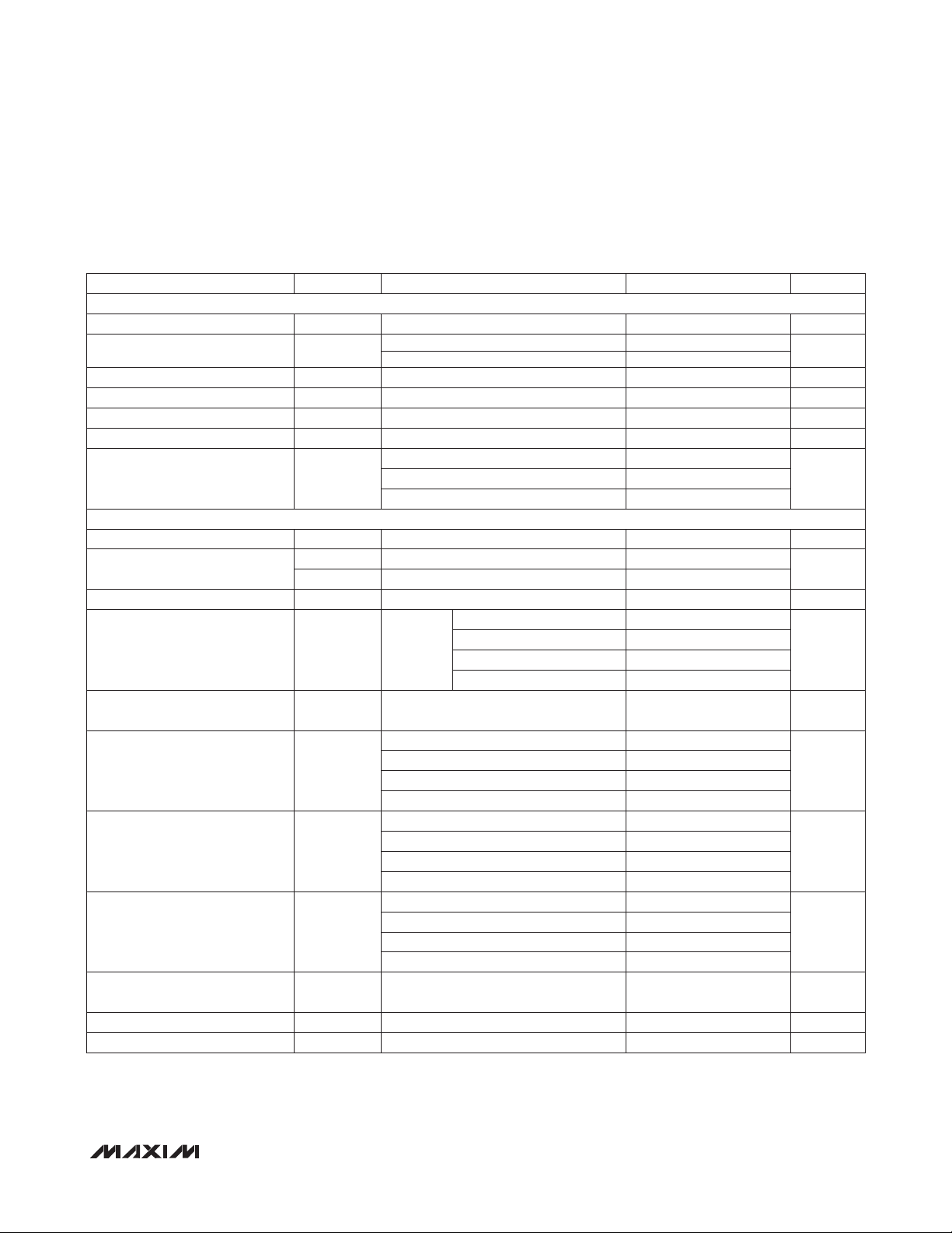
SDA
t
BUF
SCL
t
HD:STA
t
SU:DAT
t
t
t
LOW
t
HIGH
t
R
HD:DAT
t
F
SU:STA
t
HD:STA
t
SU:STO
START
CONDITION
MAX16070/MAX16071
Figure 1. SMBus Timing Diagram
t
2
TCK
TDI, TMS
t
6
t
7
t
4
REPEATED START
CONDITION
t
1
t
5
STOP
CONDITION
t
3
START
CONDITION
TDO
Figure 2. JTAG Timing Diagram
6 ______________________________________________________________________________________
Page 7
12-Channel/8-Channel, Flash-Configurable System
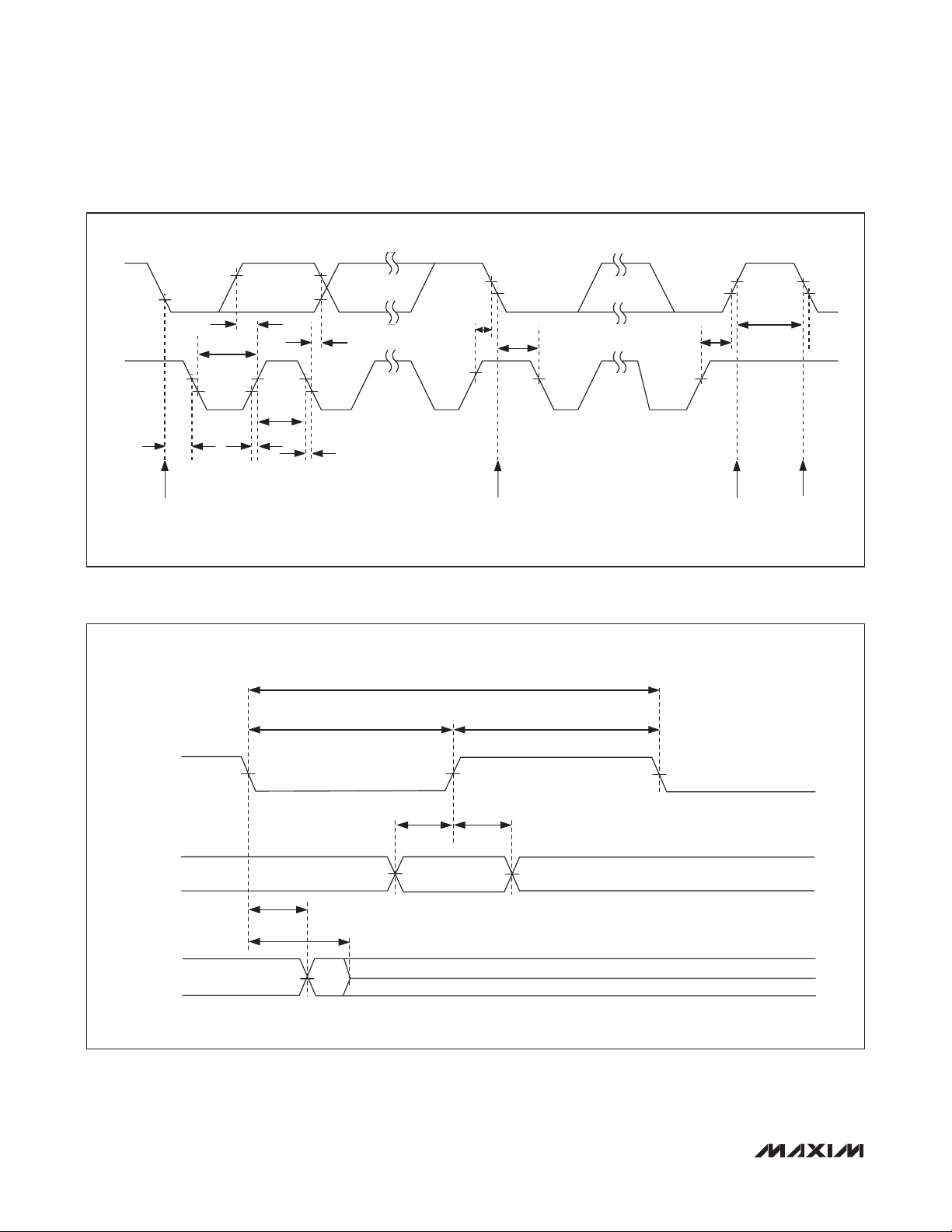
VCC SUPPLY CURRENT
NORMALIZED MON_ THRESHOLD
NORMALIZED EN THRESHOLD
NORMALIZED EN THRESHOLD
TRANSIENT DURATION
µ
NORMALIZED TIMING ACCURACY
MON_ DEGLITCH
µ
DELAY (µs)
OUTPUT VOLTAGE
OUTPUT-VOLTAGE HIGH vs.
V
(V)
Managers with Nonvolatile Fault Registers
Typical Operating Characteristics
(Typical values are at VCC = 3.3V, T
= +25°C, unless otherwise noted.)
A
MAX16070/MAX16071
6
ABP AND DBP CONNECTED TO V
5
4
(mA)
3
CC
I
2
1
0
ABP AND DBP
REGULATORS ACTIVE
FOR LOW-VOLTAGE APPLICATIONS
VCC < 3.6V CONNECT ABP AND
DBP TO V
0 14
+25NC
-40NC
CC
VCC (V)
vs. THRESHOLD OVERDRIVE (EN)
160
140
s)
120
100
80
60
TRANSIENT DURATION (
40
20
vs. VCC SUPPLY VOLTAGE
0
1 100
10
EN OVERDRIVE (mV)
CC
+85NC
12108642
1.2
1.0
MAX16070 toc01
0.8
0.6
0.4
NORMALIZED MON_ THRESHOLD
0.2
0
-40 80
5.6V RANGE,
HALF SCALE,
PUV THRESHOLD
6040200-20
TEMPERATURE (NC)
MAX16070 toc02
1.006
1.004
1.002
1.000
0.998
0.996
0.994
0.992
-40
vs. TEMPERATURE
vs. TEMPERATURE
0.986
0.984
MAX16070 toc04
0.982
0.980
0.978
0.976
NORMALIZED SLOT DELAY
0.974
0.972
-40
806040200-20
TEMPERATURE (NC)
MAX16070 toc05
120
100
s)
80
60
40
TRANSIENT DURATION (
20
0
vs. TEMPERATURE
TEMPERATURE (NC)
vs. TRANSIENT DURATION
2
4 8 16
DEGLITCH VALUE
MAX16070 toc03
806040200-20
MAX16070 toc06
2.0
1.8
1.6
1.4
1.2
1.0
0.8
0.6
0.4
0.2
0
MR TO RESET PROPAGATION DELAY
vs. TEMPERATURE
MAX
MIN
-40
TEMPERATURE (NC)
_______________________________________________________________________________________ 7
806020 400-20
MAX16070 toc07
vs. SINK CURRENT (OUT = LOW)
0.45
0.40
0.35
0.30
0.25
(V)
OUT
V
0.20
0.15
0.10
0.05
0
0 20
GPIO_
I
OUT
RESET
(mA)
SOURCE CURRENT (PUSH-PULL OUTPUT)
3.4
3.3
3.2
MAX16070 toc08
3.1
3.0
2.9
OUT
2.8
2.7
2.6
2.5
2.4
15105
0 1500
RESET
GPIO_
1000500
I
(µA)
OUT
MAX16070 toc09
Page 8
12-Channel/8-Channel Flash-Configurable System
INL (LSB)
NORMALIZED CURRENT-SENSE
CURRENT-SENSE ACCURACY
CURRENT-SENSE TRANSIENT DURATION
RESET OUTPUT CURRENT
Monitors with Nonvolatile Fault Registers
Typical Operating Characteristics (continued)
(Typical values are at VCC = 3.3V, T
= +25°C, unless otherwise noted.)
A
INTEGRAL NONLINEARITY vs. CODE
1.0
0.8
0.6
0.4
0.2
0
-0.2
-0.4
-0.6
-0.8
-1.0
0 1024
CODE (LSB)
MAX16070/MAX16071
1.05
1.03
1.01
0.99
0.97
NORMALIZED CURRENT-SENSE ACCURACY
0.95
ACCURACY vs. TEMPERATURE
200mV
100mV
-40
TEMPERATURE (NC)
25mV
6010
DIFFERENTIAL NONLINEARITY vs. CODE
1.0
0.8
MAX16070 toc10
896768512 640256 384128
0.6
0.4
0.2
0
DNL (LSB)
-0.2
-0.4
-0.6
-0.8
-1.0
0 1024
CODE (LSB)
MAX16070 toc11
896768512 640256 384128
vs. CSP-CSM VOLTAGE
1.0
0.8
MAX16070 toc12
0.6
0.4
0.2
0
ERROR (mV)
-0.2
-0.4
-0.6
-0.8
-1.0
0 30
CSP-CSMs VOLTAGE (mV)
MAX16070 toc13
252015105
8 ______________________________________________________________________________________
1.8
vs. CSP-CSM OVERDRIVE
1.6
1.4
1.2
1.0
0.8
0.6
TRANSIENT DURATION (Fs)
0.4
0.2
0
0 100
CSP-CSM OVERDRIVE (mV)
18
16
MAX16070 toc14
80604020
14
12
10
8
6
OUTPUT CURRENT (mA)
4
2
0
0 14
ABP AND DBP
CONNECTED TO V
ABP AND DBP
REGULATORS ACTIVE
SUPPLY VOLTAGE (V)
V
CC
RESET
MAX16070 toc15
= 0.3V
12106 842
vs. SUPPLY VOLTAGE
Page 9

12-Channel/8-Channel, Flash-Configurable System
Managers with Nonvolatile Fault Registers
Pin Description
MAX16070/MAX16071
PIN
MAX16070 MAX16071
1–5, 34, 35, 401–5, 37, 38,
40
6 6 CSP
7 7 CSM
8 8 RESET Configurable Reset Output
9 9 TMS JTAG Test Mode Select
10 10 TDI JTAG Test Data Input
11 11 TCK JTAG Test Clock
12 12 TDO JTAG Test Data Output
13 13 SDA SMBus Serial-Data Open-Drain Input/Output
14 14 A0 Four-State SMBus Address. Address sampled upon POR.
15 15 SCL SMBus Serial Clock Input
16, 33 16, 36 GND Ground
17, 18 — GPIO7, GPIO8
19–24 17–22 GPIO1–GPIO6
25, 26, 27, 29
28 29 EN
30 31, 32 DBP
31 33, 34 V
32 35 ABP Analog Bypass. Bypass ABP with a 1FF ceramic capacitor to GND.
36–39 —
— — EP
23–28,
30, 39
NAME FUNCTION
MON2–MON6,
MON7, MON8,
MON1
N.C. No Connection. Not internally connected.
CC
MON9–
MON12
Monitor Voltage Input 1–Monitor Voltage Input 8. Set monitor voltage range
through configuration registers. Measured value written to the ADC register
can be read back through the SMBus or JTAG interface.
Current-Sense Amplifier Positive Input. Connect CSP to the source side of the
external sense resistor.
Current-Sense Amplifier Negative Input. Connect CSM to the load side of the
external sense resistor.
General-Purpose Input/Output 7 and General-Purpose Input/Output 8.
GPIO_s can be configured to act as a TTL input, a push-pull, open-drain, or
high-impedance output or a pulldown circuit during a fault event or reverse
sequencing.
General-Purpose Input/Output 1–General-Purpose Input/Output 6. GPIO_s
can be configured to act as a TTL input, a push-pull, open-drain, or highimpedance output or a pulldown circuit during a fault event.
Analog Enable Input. All outputs deassert when VEN is below the enable
threshold.
Digital Bypass. All push-pull outputs are referenced to DBP. Bypass DBP with
a 1FF capacitor to GND.
Device Power Supply. Connect VCC to a voltage from 2.8V to 14V. Bypass
VCC with a 10FF capacitor to GND.
Monitor Voltage Input 9–Monitor Voltage Input 12. Set monitor voltage range
through configuration registers. Measured value written to the ADC register
can be read back through the SMBus or JTAG interface.
Exposed Pad. Internally connected to GND. Connect to ground, but do not
use as the main ground connection.
_______________________________________________________________________________________ 9
Page 10
12-Channel/8-Channel, Flash-Configurable System
Managers with Nonvolatile Fault Registers
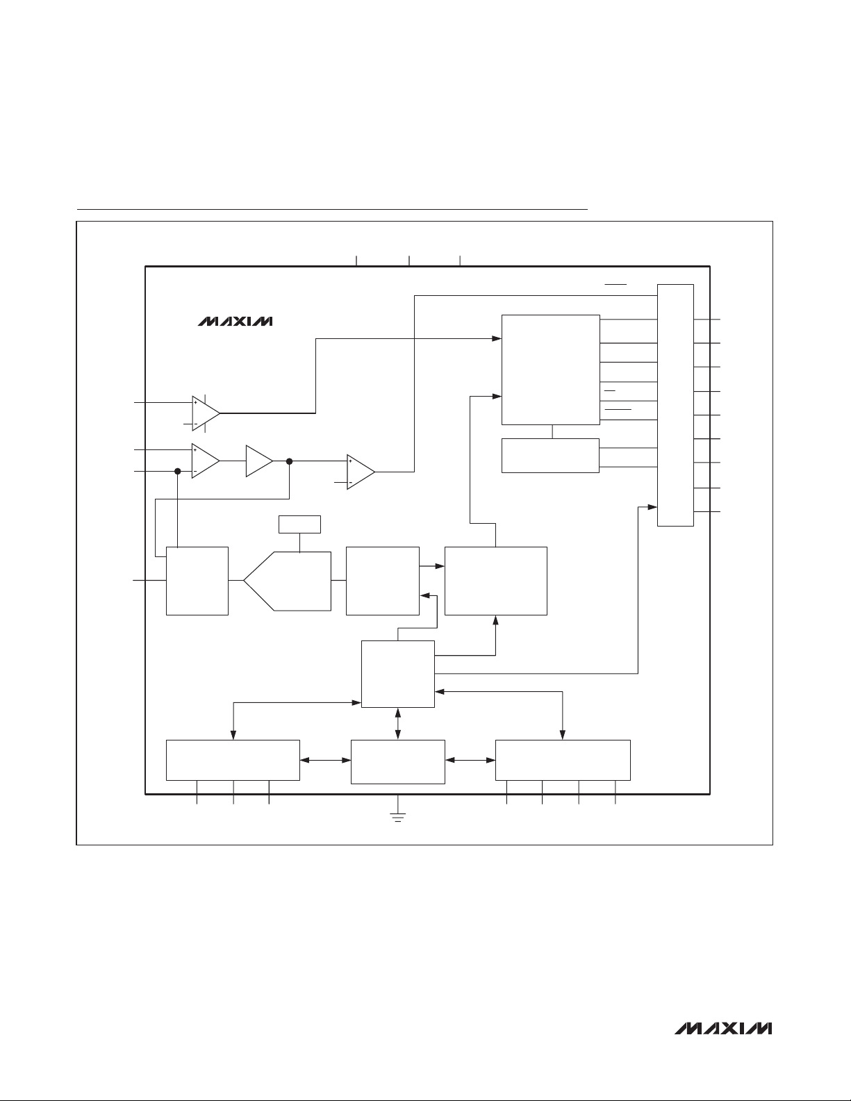
Functional Diagram
V
CC
MAX16070
MAX16071
EN
1.4V
CSP
CSM
A
V
V
CSTH
MAX16070/MAX16071
REF
MON1–
MON12
VOLTAGE
SCALING
AND
MUX
10-BIT ADC
(SAR)
REGISTERS
ADC
ABP DBP
DIGITAL
COMPARATORS
DECODE
LOGIC
WATCHDOG
TIMER
OVERC
RESET
ANYFAULT
FAULT1
FAULT2
MR
MARGIN
WDI
WDO
GPIO1–GPIO8
RESET
G
P
I
O
C
O
N
T
R
O
L
GPIO1
GPIO2
GPIO3
GPIO4
GPIO5
GPIO6
GPIO7
GPIO8
RAM
REGISTERS
SMBus INTERFACE
AO
SCL SDA
FLASH
MEMORY
GND
TDO TDI TCK TMS
JTAG
INTERFACE
10 _____________________________________________________________________________________
Page 11

12-Channel/8-Channel, Flash-Configurable System
Managers with Nonvolatile Fault Registers
Detailed Description
The MAX16070 monitors up to twelve system power supplies and the MAX16071 can monitor up to eight system
power supplies. After boot-up, if EN is high and the software enable bit is set to ‘1,’ monitoring begins based on
the configuration stored in flash. An internal multiplexer
cycles through each MON_ input. At each multiplexer
stop, the 10-bit ADC converts the monitored analog voltage to a digital result and stores the result in a register.
Each time a conversion cycle (50Fs, max) completes,
internal logic circuitry compares the conversion results
to the overvoltage and undervoltage thresholds stored in
memory. When a result violates a programmed threshold,
the conversion can be configured to generate a fault.
GPIO_ can be programmed to assert on combinations
of faults. Additionally, faults can be configured to shut off
the system and trigger the nonvolatile fault logger, which
writes all fault information automatically to the flash and
write-protects the data to prevent accidental erasure.
The MAX16070/MAX16071 contain both SMBus and
JTAG serial interfaces for accessing registers and flash.
Use only one interface at any given time. For more information on how to access the internal memory through
these interfaces, see the SMBus-Compatible Interface
and JTAG Serial Interface sections. The memory map
is divided into three pages with access controlled by
special SMBus and JTAG commands.
The factory-default values at POR (power-on reset) for all
RAM registers are ‘0’s. POR occurs when VCC reaches
the undervoltage-lockout threshold (UVLO) of 2.8V (max).
At POR, the device begins a boot-up sequence. During
the boot-up sequence, all monitored inputs are masked
from initiating faults and flash contents are copied to
the respective register locations. During boot-up, the
MAX16070/MAX16071 are not accessible through the
serial interface. The boot-up sequence takes up to
150Fs, after which the device is ready for normal operation. RESET is asserted low up to the boot-up phase and
remains asserted for its programmed timeout period once
sequencing is completed and all monitored channels
are within their respective thresholds. Up to the boot-up
phase, the GPIO_s are high impedance.
Power
Apply 2.8V to 14V to VCC to power the MAX16070/
MAX16071. Bypass VCC to ground with a 10FF capacitor. Two internal voltage regulators, ABP and DBP,
supply power to the analog and digital circuitry within
the device. For operation at 3.6V or lower, disable the
regulators by connecting ABP and DBP to VCC.
ABP is a 3.0V (typ) voltage regulator that powers the internal analog circuitry. Bypass ABP to GND with a 1FF ceramic capacitor installed as close to the device as possible.
DBP is an internal 3.0V (typ) voltage regulator. DBP powers flash and digital circuitry. All push-pull outputs refer to
DBP. Bypass the DBP output to GND with a 1FF ceramic
capacitor installed as close as possible to the device.
Do not power external circuitry from ABP or DBP.
Enable
To enable monitoring, the voltage at EN must be above
1.4V and the software enable bit in r73h[0] must be set
to ‘1.’ To power down and disable monitoring, either pull
EN below 1.35V or set the Software Enable bit to ‘0.’
See Table 1 for the software enable bit configurations.
Connect EN to ABP if not used.
MAX16070/MAX16071
Table 1. Software Enable Configurations
REGISTER
ADDRESS
73h 273h
FLASH
ADDRESS
______________________________________________________________________________________ 11
BIT RANGE DESCRIPTION
[0] Software enable
[1] Reserved
[2] 1 = Margin mode enabled
Early warning threshold select
[3]
[4]
0 = Early warning is undervoltage
1 = Early warning is overvoltage
Independent watchdog mode enable
1 = Watchdog timer is independent of sequencer
0 = Watchdog timer boots after sequence completes
Page 12
12-Channel/8-Channel, Flash-Configurable System
Managers with Nonvolatile Fault Registers
When in the monitoring state, a register bit, ENRESET,
is set to a ‘1’ when EN falls below the undervoltage
threshold. This register bit latches and must be cleared
through software. This bit indicates if RESET asserted
low due to EN going under the threshold. The POR state
of ENRESET is ‘0’. The bit is only set on a falling edge
of the EN comparator output or the software enable bit.
Voltage/Current Monitoring
The MAX16070/MAX16071 feature an internal 10-bit
ADC that monitors the MON_ voltage inputs. An internal
multiplexer cycles through each of the enabled inputs,
taking less than 40Fs for a complete monitoring cycle.
Each acquisition takes approximately 3.2Fs. At each
multiplexer stop, the 10-bit ADC converts the analog
input to a digital result and stores the result in a register.
ADC conversion results are stored in registers r00h to
r1Ah (see Table 6). Use the SMBus or JTAG serial interface to read ADC conversion results.
The MAX16070 provides twelve inputs, MON1 to MON12,
MAX16070/MAX16071
for voltage monitoring. The MAX16071 provides eight
inputs, MON1 to MON8, for voltage monitoring. Each
input voltage range is programmable in registers r43h to
r45h (see Table 5). When MON_ configuration registers
are set to ’11,’ MON_ voltages are not monitored, and
the multiplexer does not stop at these inputs, decreasing
the total cycle time. These inputs cannot be configured
to trigger fault conditions.
The three programmable thresholds for each monitored
voltage include an overvoltage, an undervoltage, and a
secondary warning threshold that can be set in r73h[3]
to be either an undervoltage or overvoltage threshold.
See the Faults section for more information on setting
overvoltage and undervoltage thresholds. All voltage
thresholds are 8 bits wide. The 8 MSBs of the 10-bit ADC
conversion result are compared to these overvoltage
and undervoltage thresholds.
Inputs that are not enabled are not converted by the
ADC; they contain the last value acquired before that
channel was disabled.
The ADC conversion result registers are reset to 00h at
boot-up. These registers are not reset when a reboot
command is executed.
Configure the MAX16070/MAX16071 for differential
mode in r46h (Table 5). The possible differential pairs
are MON1/MON2, MON3/MON4, MON5/MON6, MON7/
MON8, MON9/MON10, MON11/MON12 with the first
input always being at a higher voltage than the second.
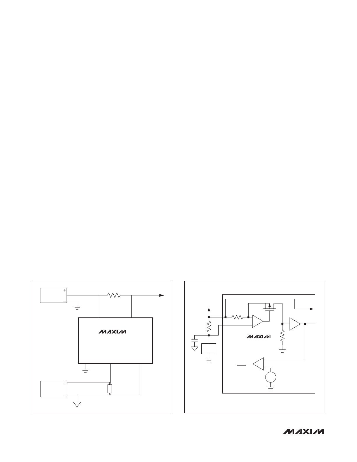
Use differential voltage sensing to eliminate voltage offsets or measure supply current. See Figure 3. In differential mode, the odd-numbered MON_ input measures
the absolute voltage with respect to GND while the result
of the even input is the difference between the odd and
even inputs. See Figure 3 for the typical differential measurement circuit.
POWER
SUPPLY
POWER
SUPPLY
MON
ODD
MAX16070
MAX16071
MON
S
ODD
LOAD
MON
EVEN
MON
EVEN
I
LOAD
R
SENSE
V
MON
LOAD
CS+
CS-
OVERC
*ADJUSTABLE BY r47h [1:0]
-
+
MAX16070
-
+
R
Figure 3. Differential Measurement Connections Figure 4. Current-Sense Amplifier
12 _____________________________________________________________________________________
TO ADC MUX
*A
V
+
*V
CSTH
-
Page 13

12-Channel/8-Channel, Flash-Configurable System
Managers with Nonvolatile Fault Registers
Boot-Up Delay
Once EN is above its threshold and the software-enable
bit is set, a boot-up delay occurs before monitoring
begins. This delay is configured in register 77h[3:0] as
shown in Tables 2 and 3.
Internal Current-Sense Amplifier
The current-sense inputs, CSP/CSM, and a currentsense amplifier facilitate power monitoring (see Figure
4). The voltage on CSP relative to GND is also monitored
by the ADC when the current-sense amplifier is enabled
with r47h[0]. The conversion results are located in registers r19h and r1Ah (see Table 6). There are two selectable voltage ranges for CSP set by r47h[1], see Table
4. Although the voltage can be monitored over SMBus
or JTAG, this voltage has no threshold comparators and
cannot trigger any faults. Regarding the current-sense
amplifier, there are four selectable ranges and the ADC
output for a current-sense conversion is:
X
where X
r18h, V
= (V
ADC
is the 8-bit decimal ADC result in register
ADC
is V
SENSE
CSP
x AV)/1.4V x (28 - 1)
SENSE
- V
and AV is the current-
CSM,
sense voltage gain set by r47h[3:2].
In addition, there are two programmable current-sense
trip thresholds: primary overcurrent and secondary overcurrent. For fast fault detection, the primary overcurrent
threshold is implemented with an analog comparator
connected to the internal OVERC signal. The OVERC
signal can be output on one of the GPIO_s. See the
General-Purpose Inputs/Outputs section for configuring the GPIO_ to output the OVERC signal. The primary
threshold is set by:
ITH = V
where ITH is the current threshold to be set, V
the threshold set by r47h[3:2], and R
CSTH/RSENSE
SENSE
is
CSTH
is the value
of the sense resistor. See Table 4 for a description of
r47h. OVERC depends only on the primary overcurrent
threshold. The secondary overcurrent threshold is implemented through ADC conversions and digital comparison set by r6Ch. The secondary overcurrent threshold
includes programmable time delay options located in
r73h[6:5]. Primary and secondary current-sense faults
are enabled/disabled through r47h[0].
MAX16070/MAX16071
Table 2. Boot-Up Delay Register
REGISTER
ADDRESS
77h 277h
FLASH
ADDRESS
BIT RANGE DESCRIPTION
Table 3. Boot-Up Delay Values
CODE VALUE
0000
0001
0010 1ms
0011 2ms
0100 3ms
0101 4ms
0110 6ms
0111 8ms
1000 10ms
1001 12ms
1010 25ms
1011 100ms
1100 200ms
1101 400ms
1110 800ms
1111 1.6s
[3:0] Boot-up delay
[7:0] Reserved
25Fs
500Fs
______________________________________________________________________________________ 13
Page 14

12-Channel/8-Channel, Flash-Configurable System
Managers with Nonvolatile Fault Registers
Table 4. Overcurrent Primary Threshold and Current-Sense Control
REGISTER
ADDRESS
47h 247h
73h 273h [6:5]
FLASH
ADDRESS
BIT
RANGE
[0]
[1]
[3:2]
1 = Current sense is enabled
0 = Current sense is disabled
1 = CSP full-scale range is 14V
0 = CSP full-scale range is 7V
Overcurrent primary threshold and current-sense gain setting
00 = 200mV threshold, AV = 6V/V
01 = 100mV threshold, AV = 12V/V
10 = 50mV threshold, AV = 24V/V
11 = 25mV threshold, AV = 48V/V
Overcurrent secondary threshold deglitch
00 = No delay
01 = 14ms
10 = 15ms
11 = 60ms
MAX16070/MAX16071
Table 5. ADC Configuration Registers
REGISTER ADDRESS
43h 243h
FLASH
ADDRESS
BIT RANGE DESCRIPTION
[1:0]
[3:2]
[5:4]
[7:6]
DESCRIPTION
ADC1 full-scale range
00 = 5.6V
01 = 2.8V
10 = 1.4V
11 = Channel not converted
ADC2 full-scale range
00 = 5.6V
01 = 2.8V
10 = 1.4V
11 = Channel not converted
ADC3 full-scale range
00 = 5.6V
01 = 2.8V
10 = 1.4V
11 = Channel not converted
ADC4 full-scale range
00 = 5.6V
01 = 2.8V
10 = 1.4V
11 = Channel not converted
14 _____________________________________________________________________________________
Page 15

12-Channel/8-Channel, Flash-Configurable System
Managers with Nonvolatile Fault Registers
Table 5. ADC Configuration Registers (continued)
MAX16070/MAX16071
REGISTER ADDRESS
44h 244h
45h 245h
FLASH
ADDRESS
BIT RANGE DESCRIPTION
ADC5 full-scale range
00 = 5.6V
[1:0]
[3:2]
[5:4]
[7:6]
[1:0]
[3:2]
[5:4]
[7:6]
01 = 2.8V
10 = 1.4V
11 = Channel not converted
ADC6 full-scale range
00 = 5.6V
01 = 2.8V
10 = 1.4V
11 = Channel not converted
ADC7 full-scale range
00 = 5.6V
01 = 2.8V
10 = 1.4V
11 = Channel not converted
ADC8 full-scale range
00 = 5.6V
01 = 2.8V
10 = 1.4V
11 = Channel not converted
ADC9 full-scale range
00 = 5.6V
01 = 2.8V
10 = 1.4V
11 = Channel not converted
ADC10 full-scale range
00 = 5.6V
01 = 2.8V
10 = 1.4V
11 = Channel not converted
ADC11 full-scale range
00 = 5.6V
01 = 2.8V
10 = 1.4V
11 = Channel not converted
ADC12 full-scale range
00 = 5.6V
01 = 2.8V
10 = 1.4V
11 = Channel not converted
______________________________________________________________________________________ 15
Page 16

12-Channel/8-Channel, Flash-Configurable System
Managers with Nonvolatile Fault Registers
Table 5. ADC Configuration Registers (continued)
REGISTER ADDRESS
46h 246h
FLASH
ADDRESS
BIT RANGE DESCRIPTION
[0]
[1]
[2]
[3]
[4]
MAX16070/MAX16071
[5]
Differential conversion ADC1, ADC2
0 = Disabled
1 = Enabled
Differential conversion ADC3, ADC4
0 = Disabled
1 = Enabled
Differential conversion ADC5, ADC6
0 = Disabled
1 = Enabled
Differential conversion ADC7, ADC8
0 = Disabled
1 = Enabled
Differential conversion ADC9, ADC10
0 = Disabled
1 = Enabled
Differential conversion ADC11, ADC12
0 = Disabled
1 = Enabled
16 _____________________________________________________________________________________
Page 17

12-Channel/8-Channel, Flash-Configurable System
Managers with Nonvolatile Fault Registers
Table 6. ADC Conversion Results (Read Only)
REGISTER ADDRESS BIT RANGE DESCRIPTION
00h [7:0] ADC1 result (MSB) bits 9–2
01h [7:6] ADC1 result (LSB) bits 1, 0
02h [7:0] ADC2 result (MSB) bits 9–2
03h [7:6] ADC2 result (LSB) bits 1, 0
04h [7:0] ADC3 result (MSB) bits 9–2
05h [7:6] ADC3 result (LSB) bits 1, 0
06h [7:0] ADC4 result (MSB) bits 9–2
07h [7:6] ADC4 result (LSB) bits 1, 0
08h [7:0] ADC5 result (MSB) bits 9–2
09h [7:6] ADC5 result (LSB) bits 1, 0
0Ah [7:0] ADC6 result (MSB) bits 9–2
0Bh [7:6] ADC6 result (LSB) bits 1, 0
0Ch [7:0] ADC7 result (MSB) bits 9–2
0Dh [7:6] ADC7 result (LSB) bits 1, 0
0Eh [7:0] ADC8 result (MSB) bits 9–2
0Fh [7:6] ADC8 result (LSB) bits 1, 0
10h [7:0] ADC9 result (MSB) bits 9–2
11h [7:6] ADC9 result (LSB) bits 1, 0
12h [7:0] ADC10 result (MSB) bits 9–2
13h [7:6] ADC10 result (LSB) bits 1, 0
14h [7:0] ADC11 result (MSB) bits 9–2
15h [7:6] ADC11 result (LSB) bits 1, 0
16h [7:0] ADC12 result (MSB) bits 9–2
17h [7:6] ADC12 result (LSB) bits 1, 0
18h [7:0] Current-sense ADC result
19h [7:0] CSP ADC output (MSB) bits 9–2
1Ah [7:6] CSP ADC output (LSB) bits 1, 0
MAX16070/MAX16071
______________________________________________________________________________________ 17
Page 18

12-Channel/8-Channel, Flash-Configurable System
Managers with Nonvolatile Fault Registers
General-Purpose Inputs/Outputs
GPIO1 to GPIO8 are programmable general-purpose
inputs/outputs. GPIO1–GPIO8 are configurable as a
manual reset input, a watchdog timer input and output,
logic inputs/outputs, fault-dependent outputs. When programmed as outputs, GPIO_s are open drain or pushpull. See Tables 8 and 9 for more detailed information on
configuring GPIO1 to GPIO8.
Table 7. GPIO_ State Registers
REGISTER
ADDRESS
1Eh —
MAX16070/MAX16071
3Eh 23Eh
FLASH
ADDRESS
BIT RANGE DESCRIPTION
[0] GPIO1 input state
[1] GPIO2 input state
[2] GPIO3 input state
[3] GPIO4 input state
[4] GPIO5 input state
[5] GPIO6 input state
[6] GPIO7 input state
[7] GPIO8 input state
[0] GPIO1 output state
[1] GPIO2 output state
[2] GPIO3 output state
[3] GPIO4 output state
[4] GPIO5 output state
[5] GPIO6 output state
[6] GPIO7 output state
[7] GPIO8 output state
When GPIO1 to GPIO8 are configured as general-purpose inputs/outputs, read values from the GPIO_ ports
through r1Eh and write values to GPIO_s through r3Eh.
Note that r3Eh has a corresponding flash register, which
programs the default state of a general-purpose output.
See Table 7 for more information on reading and writing
to the GPIO_.
Table 8. GPIO_ Configuration Registers
REGISTER
ADDRESS
3Fh 23Fh
40h 240h
41h 241h
18 _____________________________________________________________________________________
FLASH
ADDRESS
BIT RANGE DESCRIPTION
[2:0] GPIO1 configuration
[5:3] GPIO2 configuration
[7:6] GPIO3 configuration (LSB)
[0] GPIO3 configuration (MSB)
[3:1] GPIO4 configuration
[6:4] GPIO5 configuration
[7] GPIO6 configuration (LSB)
[1:0] GPIO6 configuration (MSB)
[4:2] GPIO7 configuration
[7:5] GPIO8 configuration
Page 19

12-Channel/8-Channel, Flash-Configurable System
Managers with Nonvolatile Fault Registers
Table 8. GPIO_ Configuration Registers (continued)
MAX16070/MAX16071
REGISTER
ADDRESS
42h 242h
FLASH
ADDRESS
BIT RANGE DESCRIPTION
Output configuration for GPIO1
[0]
[1]
[2]
[3]
[4]
[5]
[6]
[7]
0 = Push-pull
1 = Open drain
Output configuration for GPIO2
0 = Push-pull
1 = Open drain
Output configuration for GPIO3
0 = Push-pull
1 = Open drain
Output configuration for GPIO4
0 = Push-pull
1 = Open drain
Output configuration for GPIO5
0 = Push-pull
1 = Open drain
Output configuration for GPIO6
0 = Push-pull
1 = Open drain
Output configuration for GPIO7
0 = Push-pull
1 = Open drain
Output configuration for GPIO8
0 = Push-pull
1 = Open drain
Table 9. GPIO_ Function Configuration Bits
CODE GPIO1 GPIO2 GPIO3 GPIO4 GPIO5 GPIO6 GPIO7 GPIO8
000 Logic input
001 Logic output
010 Fault2 output
011 Fault1 output
100
101
110 MR input
111 WDI input — —
ANY_FAULT
output
OVERC
output
______________________________________________________________________________________ 19
Logic
input
Logic
output
Fault2
output
Fault1
output
—
OVERC
output
WDO
output
Logic input Logic input Logic input
Logic output Logic output Logic output
Fault2 output Fault2 output Fault2 output
— Fault1 output Fault1 output
ANY_FAULT
output
OVERC
output
MR input WDO output MR input
ANY_FAULT
output
OVERC
output
EXTFAULT
input/output
ANY_FAULT
output
OVERC
output
—
Logic
input
Logic
output
Fault2
output
Fault1
output
—
OVERC
output
WDO
output
MARGIN
input
Logic input Logic input
Logic output Logic output
Fault2 output
Fault1 output
ANY_FAULT
output
OVERC
output
MR input WDO output
—
Fault2
output
FAULT
output
OVERC
output
EXTFAULT
input/output
—
Page 20

12-Channel/8-Channel, Flash-Configurable System
Managers with Nonvolatile Fault Registers
Fault1 and Fault2
GPIO1 to GPIO8 are configurable as dedicated fault outputs, Fault1 or Fault2. Fault outputs can assert on one or
more overvoltage, undervoltage, or early warning conditions for selected inputs, as well as the secondary overcurrent comparator. Fault1 and Fault2 dependencies
Table 10. Fault1 and Fault2 Dependencies
REGISTER
ADDRESS
36h 236h
MAX16070/MAX16071
37h 237h
38h 238h
FLASH
ADDRESS
BIT
RANGE
0 1 = Fault1 depends on MON1
1 1 = Fault1 depends on MON2
2 1 = Fault1 depends on MON3
3 1 = Fault1 depends on MON4
4 1 = Fault1 depends on MON5
5 1 = Fault1 depends on MON6
6 1 = Fault1 depends on MON7
7 1 = Fault1 depends on MON8
0 1 = Fault1 depends on MON9
1 1 = Fault1 depends on MON10
2 1 = Fault1 depends on MON11
3 1 = Fault1 depends on MON12
4
5
6
7
[0] 1 = Fault2 depends on MON1
[1] 1 = Fault2 depends on MON2
[2] 1 = Fault2 depends on MON3
[3] 1 = Fault2 depends on MON4
[4] 1 = Fault2 depends on MON5
[5] 1 = Fault2 depends on MON6
[6] 1 = Fault2 depends on MON7
[7] 1 = Fault2 depends on MON8
1 = Fault1 depends on the overvoltage thresholds of the inputs selected by
r36h and r37h[3:0]
1 = Fault1 depends on the undervoltage thresholds of the inputs selected by
r36h and r37h[3:0]
1 = Fault1 depends on the early warning thresholds of the inputs selected by
r36h and r37h[3:0]
0 = Fault1 is an active-low digital output
1 = Fault1 is an active-high digital output
are set using registers r36h to r3Ah. See Table 10. When
a fault output depends on more than one MON_, the
fault output asserts when one or more MON_ exceeds a
programmed threshold voltage. These fault outputs act
independently of the critical fault system, described in
the Critical Faults section.
DESCRIPTION
20 _____________________________________________________________________________________
Page 21

12-Channel/8-Channel, Flash-Configurable System
Managers with Nonvolatile Fault Registers
Table 10. Fault1 and Fault2 Dependencies (continued)
REGISTER
ADDRESS
39h 239h
3Ah 23Ah
FLASH
ADDRESS
BIT
RANGE
[0] 1 = Fault2 depends on MON9
[1] 1 = Fault2 depends on MON10
[2] 1 = Fault2 depends on MON11
[3] 1 = Fault2 depends on MON12
[4]
[5]
[6]
[7]
[0] 1 = Fault1 depends on secondary overcurrent comparator
[1] 1 = Fault2 depends on secondary overcurrent comparator
[7:2] Reserved
1 = Fault2 depends on the overvoltage thresholds of the inputs selected by
r38h and r39h[3:0]
1 = Fault2 depends on the undervoltage thresholds of the inputs selected by
r38h and r39h[3:0]
1 = Fault2 depends on the early warning thresholds of the inputs selected by
r38h and r39h[3:0]
0 = Fault2 is an active-low digital output
1 = Fault2 is an active-high digital output
DESCRIPTION
MAX16070/MAX16071
ANY_FAULT
GPIO1, GPIO3, GPIO4, GPIO5, and GPIO7 are configurable to assert low during any fault condition.
Overcurrent Comparator (OVERC)
GPIO1 to GPIO8 are configurable to assert low when
the voltage across CSP and CSM exceed the primary
overcurrent threshold. See the Internal Current-Sense
Amplifier section for more details.
Manual Reset (MR)
GPIO1, GPIO3, GPIO5, and GPIO7 are configurable to act
as an active-low manual reset input, MR. Drive MR low to
assert RESET. RESET remains asserted for the selected
reset timeout period after MR transitions from low to high.
Watchdog Input (WDI) and Output (WDO)
GPIO2, GPIO4, GPIO6, and GPIO8 are configurable as
the watchdog timer output, WDO. GPIO1 is configurable
as WDI. See Table 17 for configuration details. WDO is an
active-low output. See the Watchdog Timer section for more
information about the operation of the watchdog timer.
External Fault (EXTFAULT)
GPIO4 and GPIO8 are configurable as the external fault
input/output. When configured as push-pull, EXTFAULT
signals that a critical fault has occurred on one or more
monitored voltages or current. When configured as
open-drain, EXTFAULT can be asserted low by an external circuit to trigger a critical fault. This signal can be
used to cascade multiple MAX16070/MAX16071s.
One configuration bit determines the behavior of the
MAX16070/MAX16071 when EXTFAULT is pulled low by
some other device. If register bit r6Dh[2] is set, EXTFAULT
going low triggers a nonvolatile fault log operation.
Faults
The MAX16070/MAX16071 monitor the input (MON_)
channels and compare the results with an overvoltage
threshold, an undervoltage threshold, and a selectable
overvoltage or undervoltage early warning threshold.
Based on these conditions, the MAX16070/MAX16071
assert various fault outputs and save specific information about the channel conditions and voltages into the
nonvolatile flash. Once a critical fault event occurs, the
failing channel condition, ADC conversions at the time of
the fault, or both can be saved by configuring the event
logger. The event logger records a single failure in the
internal flash and sets a lock bit that protects the stored
fault data from accidental erasure on a subsequent
power-up.
An overvoltage event occurs when the voltage at a monitored input exceeds the overvoltage threshold for that
input. An undervoltage event occurs when the voltage
at a monitored input falls below the undervoltage threshold. Fault thresholds are set in registers r48h to r6Ch as
shown in Table 11. Disabled inputs are not monitored for
fault conditions and are skipped over by the input multiplexer. Only the upper 8 bits of a conversion result are
compared with the programmed fault thresholds.
______________________________________________________________________________________ 21
Page 22

12-Channel/8-Channel, Flash-Configurable System
Managers with Nonvolatile Fault Registers
Table 11. Fault Threshold Registers
REGISTER
ADDRESS
48h 248h [7:0] MON1 secondary threshold
49h 249h [7:0] MON1 overvoltage threshold
4Ah 24Ah [7:0] MON1 undervoltage threshold
4Bh 24Bh [7:0] MON2 secondary threshold
4Ch 24Ch [7:0] MON2 overvoltage threshold
4Dh 24Dh [7:0] MON2 undervoltage threshold
4Eh 24Eh [7:0] MON3 secondary threshold
4Fh 24Fh [7:0] MON3 overvoltage threshold
50h 250h [7:0] MON3 undervoltage threshold
51h 251h [7:0] MON4 secondary threshold
52h 252h [7:0] MON4 overvoltage threshold
53h 253h [7:0] MON4 undervoltage threshold
54h 254h [7:0] MON5 secondary threshold
MAX16070/MAX16071
55h 255h [7:0] MON5 overvoltage threshold
56h 256h [7:0] MON5 undervoltage threshold
57h 257h [7:0] MON6 secondary threshold
58h 258h [7:0] MON6 overvoltage threshold
59h 259h [7:0] MON6 undervoltage threshold
5Ah 25Ah [7:0] MON7 secondary threshold
5Bh 25Bh [7:0] MON7 overvoltage threshold
5Ch 25Ch [7:0] MON7 undervoltage threshold
5Dh 25Dh [7:0] MON8 secondary threshold
5Eh 25Eh [7:0] MON8 overvoltage threshold
5Fh 25Fh [7:0] MON8 undervoltage threshold
60h 260h [7:0] MON9 secondary threshold
61h 261h [7:0] MON9 overvoltage threshold
62h 262h [7:0] MON9 undervoltage threshold
63h 263h [7:0] MON10 secondary threshold
64h 264h [7:0] MON10 overvoltage threshold
65h 265h [7:0] MON10 undervoltage threshold
66h 266h [7:0] MON11 secondary threshold
67h 267h [7:0] MON11 overvoltage threshold
68h 268h [7:0] MON11 undervoltage threshold
69h 269h [7:0] MON12 secondary threshold
6Ah 26Ah [7:0] MON12 overvoltage threshold
6Bh 26Bh [7:0] MON12 undervoltage threshold
6Ch 26Ch [7:0] Secondary overcurrent threshold
FLASH
ADDRESS
BIT RANGE DESCRIPTION
22 _____________________________________________________________________________________
Page 23

12-Channel/8-Channel, Flash-Configurable System
Managers with Nonvolatile Fault Registers
The general-purpose inputs/outputs (GPIO1 to GPIO8)
can be configured as ANY_FAULT outputs or dedicated
Fault1 and Fault2 outputs to indicate fault conditions.
These fault outputs are not masked by the critical fault
enable bits shown in Table 14. See the General-Purpose
Inputs/Outputs section for more information on configuring GPIO_s as fault outputs.
Deglitch
Fault conditions are detected at the end of each conversion. When the voltage on an input falls outside a monitored threshold for one acquisition, the input multiplexer
remains on that channel and performs several successive conversions. To trigger a fault, the input must stay
Table 12. Deglitch Configuration
outside the threshold for a certain number of acquisitions
as determined by the deglitch setting in r73h[6:5] and
r74h[6:5] (see Table 12).
Fault Flags
Fault flags indicate the fault status of a particular input.
The fault flag of any monitored input in the device can be
read at any time from registers r1Bh and r1Ch, as shown
in Table 13. Clear a fault flag by writing a ‘1’ to the appropriate bit in the flag register. Unlike the fault signals sent
to the fault outputs, these bits are masked by the Critical
Fault Enable bits (see Table 14). The fault flag is only set
when the matching enable bit in the critical fault enable
register is also set.
MAX16070/MAX16071
REGISTER
ADDRESS
73h 273h [6:5]
74h 274h [6:5]
ADDRESS
Table 13. Fault Flags
REGISTER
ADDRESS
1Bh
1Ch
FLASH
BIT RANGE DESCRIPTION
[0] MON1
[1] MON2
[2] MON3
[3] MON4
[4] MON5
[5] MON6
[6] MON7
[7] MON8
[0] MON9
[1] MON10
[2] MON11
[3] MON12
[4] Overcurrent
[5] External fault (EXTFAULT)
[6] SMB alert
BIT RANGE DESCRIPTION
Overcurrent comparator deglitch time
00 = No deglitch
01 = 4ms
10 = 15ms
11 = 60ms
Voltage comparator deglitch configuration
00 = 2 cycles
01 = 4 cycles
10 = 8 cycles
11 = 16 cycles
______________________________________________________________________________________ 23
Page 24

12-Channel/8-Channel, Flash-Configurable System
Managers with Nonvolatile Fault Registers
Table 14. Critical Fault Configuration
REGISTER
ADDRESS
6Dh 26Dh
6Eh 26Eh
MAX16070/MAX16071
6Fh 26Fh
70h 270h
71h 271h
FLASH
ADDRESS
BIT
RANGE
Fault information to log
00 = Save failed line flags and ADC values in flash
[1:0]
[2] 1 = Fault log triggered when EXTFAULT is pulled low externally
[7:3] Not used
[0] 1 = Fault log triggered when MON1 is below its undervoltage threshold
[1] 1 = Fault log triggered when MON2 is below its undervoltage threshold
[2] 1 = Fault log triggered when MON3 is below its undervoltage threshold
[3] 1 = Fault log triggered when MON4 is below its undervoltage threshold
[4] 1 = Fault log triggered when MON5 is below its undervoltage threshold
[5] 1 = Fault log triggered when MON6 is below its undervoltage threshold
[6] 1 = Fault log triggered when MON7 is below its undervoltage threshold
[7] 1 = Fault log triggered when MON8 is below its undervoltage threshold
[0] 1 = Fault log triggered when MON9 is below its undervoltage threshold
[1] 1 = Fault log triggered when MON10 is below its undervoltage threshold
[2] 1 = Fault log triggered when MON11 is below its undervoltage threshold
[3] 1 = Fault log triggered when MON12 is below its undervoltage threshold
[4] 1 = Fault log triggered when MON1 is above its overvoltage threshold
[5] 1 = Fault log triggered when MON2 is above its overvoltage threshold
[6] 1 = Fault log triggered when MON3 is above its overvoltage threshold
[7] 1 = Fault log triggered when MON4 is above its overvoltage threshold
[0] 1 = Fault log triggered when MON5 is above its overvoltage threshold
[1] 1 = Fault log triggered when MON6 is above its overvoltage threshold
[2] 1 = Fault log triggered when MON7 is above its overvoltage threshold
[3] 1 = Fault log triggered when MON8 is above its overvoltage threshold
[4] 1 = Fault log triggered when MON9 is above its overvoltage threshold
[5] 1 = Fault log triggered when MON10 is above its overvoltage threshold
[6] 1 = Fault log triggered when MON11 is above its overvoltage threshold
[7] 1 = Fault log triggered when MON12 is above its overvoltage threshold
[0] 1 = Fault log triggered when MON1 is above/below the early threshold warning
[1] 1 = Fault log triggered when MON2 is above/below the early threshold warning
[2] 1 = Fault log triggered when MON3 is above/below the early threshold warning
[3] 1 = Fault log triggered when MON4 is above/below the early threshold warning
[4] 1 = Fault log triggered when MON5 is above/below the early threshold warning
[5] 1 = Fault log triggered when MON6 is above/below the early threshold warning
[6] 1 = Fault log triggered when MON7 is above/below the early threshold warning
[7] 1 = Fault log triggered when MON8 is above/below the early threshold warning
01 = Save only failed line flags in flash
10 = Save only ADC values in flash
11 = Do not save anything
DESCRIPTION
24 _____________________________________________________________________________________
Page 25

12-Channel/8-Channel, Flash-Configurable System
Managers with Nonvolatile Fault Registers
Table 14. Critical Fault Configuration (continued)
MAX16070/MAX16071
REGISTER
ADDRESS
72h 272h
FLASH
ADDRESS
BIT
RANGE
[0] 1 = Fault log triggered when MON9 is above/below the early threshold warning
[1] 1 = Fault log triggered when MON10 is above/below the early threshold warning
[2] 1 = Fault log triggered when MON11 is above/below the early threshold warning
[3] 1 = Fault log triggered when MON12 is above/below the early threshold warning
[4] 1 = Fault log triggered when overcurrent early threshold is exceeded
[5] Reserved, must be set to ‘1’
[7:6] Reserved
If a GPIO_ is configured as an open-drain EXTFAULT
input/output, and EXTFAULT is pulled low by an external
circuit, bit r1Ch[5] is set.
The SMB Alert bit is set if the MAX16070/MAX16071
have asserted the SMBus Alert output. Clear by writing a
‘1’. See SMBALERT section for more details.
Critical Faults
During normal operation, a fault condition can be configured to store fault information in the flash memory by
setting the appropriate critical fault enable bits. Set the
appropriate critical fault enable bits in registers r6Eh to r72h
(see Table 14) for a fault condition to trigger a critical fault.
DESCRIPTION
Logged fault information is stored in flash registers r200h
to r20Fh (see Table 15). After fault information is logged,
the flash is locked and must be unlocked to enable a
new fault log to be stored. Write a ‘0’ to r8Ch[1] to unlock
the fault flash. Fault information can be configured to
store ADC conversion results and/or fault flags in registers. Select the critical fault configuration in r6Dh[1:0].
Set r6Dh[1:0] to ‘11’ to turn off the fault logger. All stored
ADC results are 8 bits wide.
Table 15. Nonvolatile Fault Log Registers
FLASH ADDRESS BIT RANGE DESCRIPTION
200h — Reserved
[0] Fault log triggered on MON1
[1] Fault log triggered on MON2
[2] Fault log triggered on MON3
201h
202h
______________________________________________________________________________________ 25
[3] Fault log triggered on MON4
[4] Fault log triggered on MON5
[5] Fault log triggered on MON6
[6] Fault log triggered on MON7
[7] Fault log triggered on MON8
[0] Fault log triggered on MON9
[1] Fault log triggered on MON10
[2] Fault log triggered on MON11
[3] Fault log triggered on MON12
[4] Fault log triggered on overcurrent
[5] Fault log triggered on EXTFAULT
[7:6] Not used
Page 26

12-Channel/8-Channel, Flash-Configurable System
Managers with Nonvolatile Fault Registers
Table 15. Nonvolatile Fault Log Registers (continued)
FLASH ADDRESS BIT RANGE DESCRIPTION
203h [7:0] MON1 ADC output
204h [7:0] MON2 ADC output
205h [7:0] MON3 ADC output
206h [7:0] MON4 ADC output
207h [7:0] MON5 ADC output
208h [7:0] MON6 ADC output
209h [7:0] MON7 ADC output
20Ah [7:0] MON8 ADC output
20Bh [7:0] MON9 ADC output
20Ch [7:0] MON10 ADC output
20Dh [7:0] MON11 ADC output
20Eh [7:0] MON12 ADC output
20Fh [7:0] Current-sense ADC output
MAX16070/MAX16071
The reset output, RESET, indicates the status of the monitored inputs.
During normal monitoring, RESET can be configured to
assert when any combination of MON_ inputs violates
configurable combinations of thresholds: undervoltage,
overvoltage, or early warning. Select the combination of
thresholds using r3Bh[1:0], and select the combination
of MON_ inputs using rCh[7:1] and r3Dh[4:0]. Note that
MON_ inputs configured as critical faults will always cause
RESET to assert regardless of these configuration bits.
RESET can be configured as push-pull or open drain
using r3Bh[3], and active-high or active-low using
r3Bh[2]. Select the reset timeout by loading a value from
Table 16 into r3Bh[7:4]. RESET can be forced to assert
by writing a ‘1’ into r3Ch[0]. RESET remains asserted
for the reset timeout period after a ‘0’ is written into
r3Ch[0]. See Table 16. The current state of RESET can
be checked by reading r20h[0].
Reset Output
Watchdog Timer
The watchdog timer operates together with or independently of the MAX16070/MAX16071. When operating in
dependent mode, the watchdog is not activated until EN
goes high and RESET is deasserted. When operating in
independent mode, the watchdog timer activates immediately after VCC exceeds the UVLO threshold and the
boot phase is complete. Set r73h[4] to ‘0’ to configure
the watchdog in dependent mode. Set r73h[4] to ‘1’ to
configure the watchdog in independent mode. See Table
17 for more information on configuring the watchdog
timer in dependent or independent mode.
Dependent Watchdog Timer Operation
Use the watchdog timer to monitor FP activity in two
modes. Flexible timeout architecture provides an adjustable watchdog startup delay of up to 300s, allowing complicated systems to complete lengthy boot-up
routines. An adjustable watchdog timeout allows the
supervisor to provide quick alerts when processor activity fails. After each reset event (VCC drops below UVLO
then returns above UVLO, software reboot, manual reset
(MR), EN input going low then high, or watchdog reset),
the watchdog startup delay provides an extended time
for the system to power up and fully initialize all FP and
system components before assuming responsibility for
routine watchdog updates. Set r76h[6:4] to a value other
than ‘000’ to enable the watchdog startup delay. Set
r76h[6:4] to ‘000’ to disable the watchdog startup delay.
26 _____________________________________________________________________________________
Page 27

12-Channel/8-Channel, Flash-Configurable System
Managers with Nonvolatile Fault Registers
Table 16. Reset Output Configuration
MAX16070/MAX16071
REGISTER
ADDRESS
3Bh 23Bh
3Ch 23Ch
3Dh 23Dh
FLASH
ADDRESS
BIT RANGE DESCRIPTION
Reset output depends on:
00 = Undervoltage threshold violations
[1:0]
[2]
[3]
[7:4]
[0]
[1] 1 = RESET depends on MON1
[2] 1 = RESET depends on MON2
[3] 1 = RESET depends on MON3
[4] 1 = RESET depends on MON4
[5] 1 = RESET depends on MON5
[6] 1 = RESET depends on MON6
[7] 1 = RESET depends on MON7
[0] 1 = RESET depends on MON8
[1] 1 = RESET depends on MON9
[2] 1 = RESET depends on MON10
[3] 1 = RESET depends on MON11
[4] 1 = RESET depends on MON12
[7:5] Reserved
01 = Early warning threshold violations
10 = Overvoltage threshold violations
11 = Undervoltage or overvoltage threshold violations
0 = Active-low
1 = Active-high
0 = Push-pull
1 = Open drain
Reset timeout period
0000 = 25μs
0001 = 1.5ms
0010 = 2.5ms
0011 = 4ms
0100 = 6ms
0101 = 10ms
0110 = 15ms
0111 = 25ms
1000 = 40ms
1001 = 60ms
1010 = 100ms
1011 = 150ms
1100 = 250ms
1101 = 400ms
1110 = 600ms
1111 = 1s
Reset soft trigger
0 = Normal RESET behavior
1 = Force RESET to assert
______________________________________________________________________________________ 27
Page 28

12-Channel/8-Channel, Flash-Configurable System
Managers with Nonvolatile Fault Registers
Table 17. Watchdog Configuration
REGISTER
ADDRESS
73h 273h [4]
MAX16070/MAX16071
76h 276h
FLASH
ADDRESS
BIT RANGE DESCRIPTION
1 = Independent mode
0 = Dependent mode
[7]
[6:4]
[3:0]
1 = Watchdog affects RESET output
0 = Watchdog does not affect RESET output
Watchdog startup delay
000 = No initial timeout
001 = 30s
010 = 40s
011 = 80s
100 = 120s
101 = 160s
110 = 220s
111 = 300s
Watchdog timeout
0000 = Watchdog disabled
0001 = 1ms
0010 = 2ms
0011 = 4ms
0100 = 8ms
0101 = 14ms
0110 = 27ms
0111 = 50ms
1000 = 100ms
1001 = 200ms
1010 = 400ms
1011 = 750ms
1100 = 1.4s
1101 = 2.7s
1110 = 5s
1111 = 10s
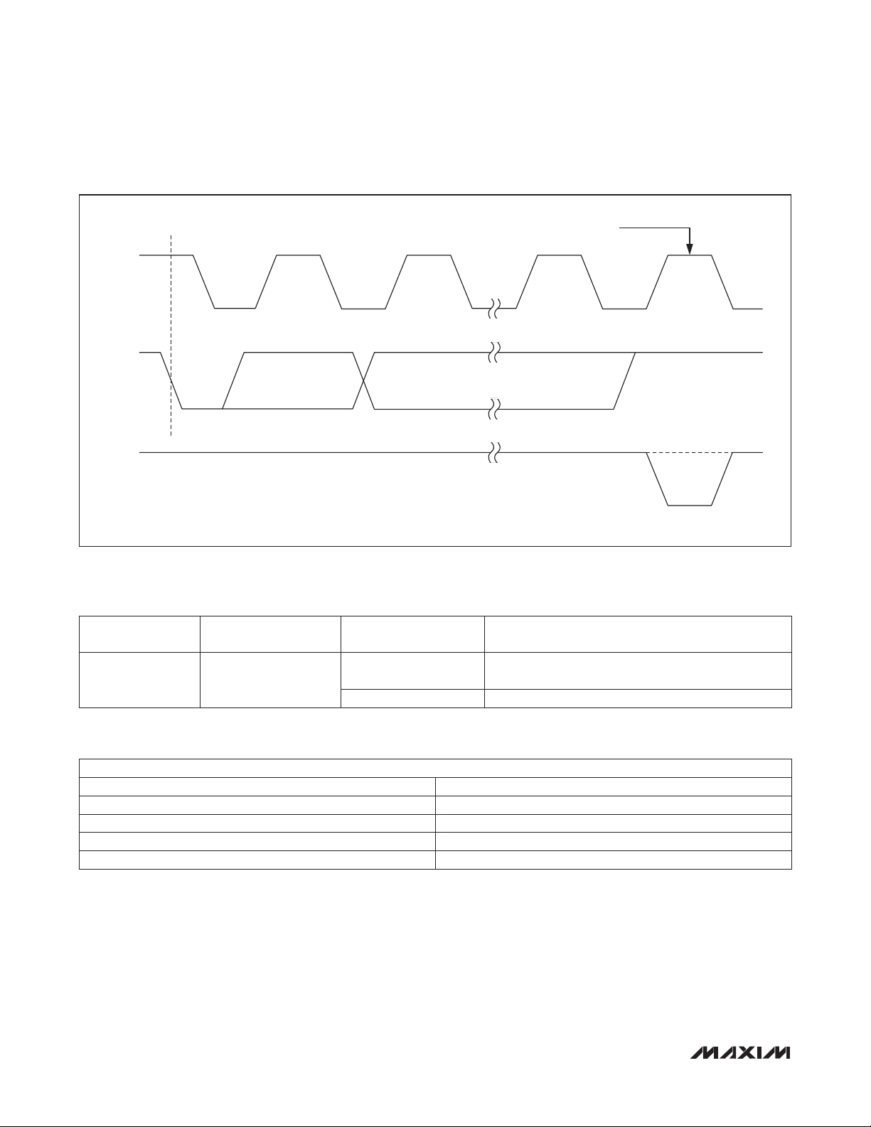
The normal watchdog timeout period, t
the first transition on WDI before the conclusion of the
long startup watchdog period, t
WDI_STARTUP
During the normal operating mode, WDO asserts if the
FP does not toggle WDI with a valid transition (high-tolow or low-to-high) within the standard timeout period,
t
. WDO remains asserted until WDI is toggled or
WDI
RESET is asserted (Figure 6).
While EN is low, the watchdog timer is in reset. The
watchdog timer does not begin counting until RESET is
deasserted. The watchdog timer is reset and WDO deas-
serts any time RESET is asserted (Figure 7). The watchdog timer will be held in reset while RESET is asserted.
28 _____________________________________________________________________________________
, begins after
WDI
(Figure 5).
The watchdog can be configured to control the RESET
output as well as the WDO output. RESET asserts for
the reset timeout, tRP, when the watchdog timer expires
and the Watchdog Reset Output Enable bit (r76h[7]) is
set to ‘1.’ When RESET is asserted, the watchdog timer
is cleared and WDO is deasserted, therefore, WDO
pulses low for a short time (approximately 1Fs) when
the watchdog timer expires. RESET is not affected by
the watchdog timer when the Watchdog Reset Output
Enable bit (r76h[7]) is set to ‘0.’ If a RESET is asserted
by the watchdog timeout, the WDRESET bit is set to ‘1’. A
connected processor can check this bit to see the reset
was due to a watchdog timeout. See Table 17 for more
information on configuring watchdog functionality.
Page 29

12-Channel/8-Channel, Flash-Configurable System
Managers with Nonvolatile Fault Registers
V
LAST MON_
TH
< t
WDI
MAX16070/MAX16071
WDI
RESET
Figure 5. Normal Watchdog Startup Sequence
V
CC
WDI
WDO
0V
V
CC
0V
< t
< t
WDI
WDI
< t
WDI
t
WDI_STARTUP
< t
WDI
t
RP
> t
WDI
t
WDI
< t
< t
WDI
WDI
< t
WDI
Figure 6. Watchdog Timer Operation
V
CC
< t
WDI
V
RESET
V
WDO
WDI
0V
CC
0V
CC
0V
t
WDI
1µs
t
RP
Figure 7. Watchdog Startup Sequence with Watchdog Reset Enable Bit Set to ‘1’
______________________________________________________________________________________ 29
< t
WDI_STARTUP
< t
WDI
Page 30

12-Channel/8-Channel, Flash-Configurable System
Managers with Nonvolatile Fault Registers
Independent Watchdog Timer Operation
When r73h[3] is ‘1’ the watchdog timer operates in
the independent mode. In the independent mode, the
watchdog timer operates as if it were a separate device.
The watchdog timer is activated immediately upon VCC
exceeding UVLO and once the boot-up sequence is finished. When RESET is asserted, the watchdog timer and
WDO are not affected.
There will be a startup delay if r76h[6:4] is set to a value
different than ‘000.’ If r76h[6:4] is set to ‘000,’ there will
not be a startup delay. See Table 17 for delay times.
In independent mode, if the Watchdog Reset Output
Enable bit r76h[7] is set to ‘1,’ when the watchdog timer
expires, WDO asserts then RESET asserts. WDO will
then deassert. WDO will be low for approximately 1Fs.
If the Watchdog Reset Output Enable bit (r76h[7]) is set
to ‘0,’ when the WDT expires, WDO asserts but RESET
is not affected.
MAX16070/MAX16071
Register r8Ah provides storage space for a user-defined
configuration or firmware version number. Note that this
register controls the contents of the JTAG USERCODE
register bits 7:0. The user-defined register is stored at
r28Ah in the flash memory.
User-Defined Register
Memory Lock Bits
Register r8Ch contains the lock bits for the configuration
registers, configuration flash, user flash, and fault register lock. See Table 18 for details.
SMBus-Compatible Interface
The MAX16070/MAX16071 feature an SMBuscompatible, 2-wire serial interface consisting of a serialdata line (SDA) and a serial-clock line (SCL). SDA and
SCL facilitate bidirectional communication between the
MAX16070/MAX16071 and the master device at clock
rates up to 400kHz. Figure 1 shows the 2-wire interface
timing diagram. The MAX16070/MAX16071 are transmit/
receive slave-only devices, relying upon a master device
to generate a clock signal. The master device (typically
a microcontroller) initiates a data transfer on the bus and
generates SCL to permit that transfer.
A master device communicates to the MAX16070/
MAX16071 by transmitting the proper address followed
by a command and/or data words. The slave address
input, A0, is capable of detecting four different states,
allowing multiple identical devices to share the same
serial bus. The slave address is described further in
the Slave Address section. Each transmit sequence is
framed by a START (S) or REPEATED START (SR) condition and a STOP (P) condition. Each word transmitted
over the bus is 8 bits long and is always followed by an
acknowledge pulse. SCL is a logic input, while SDA is
an open-drain input/output. SCL and SDA both require
external pullup resistors to generate the logic-high voltage. Use 4.7kI for most applications.
Table 18. Memory Lock Bits
REGISTER
ADDRESS
8Ch 28Ch
30 _____________________________________________________________________________________
FLASH ADDRESS BIT RANGE DESCRIPTION
Configuration register lock
0
1
2
3
1 = Locked
0 = Unlocked
Flash fault register lock
1 = Locked
0 = Unlocked
Flash configuration lock
1 = Locked
0 = Unlocked
User flash lock
1 = Locked
0 = Unlocked
Page 31

12-Channel/8-Channel, Flash-Configurable System
Managers with Nonvolatile Fault Registers
MAX16070/MAX16071
SDA
SCL
DATA LINE STABLE,
DATA VALID
Figure 8. Bit Transfer Figure 9. START and STOP Conditions
CHANGE OF
DATA ALLOWED
SDA
SCL
START
CONDITION
Bit Transfer
Each clock pulse transfers one data bit. The data on
SDA must remain stable while SCL is high (Figure 8);
otherwise the MAX16070/MAX16071 register a START or
STOP condition (Figure 9) from the master. SDA and SCL
idle high when the bus is not busy.
START and STOP Conditions
Both SCL and SDA idle high when the bus is not busy.
A master device signals the beginning of a transmission
with a START condition by transitioning SDA from high to
low while SCL is high. The master device issues a STOP
condition by transitioning SDA from low to high while
SCL is high. A STOP condition frees the bus for another
transmission. The bus remains active if a REPEATED
START condition is generated, such as in the block read
protocol (see Figure 1).
The acknowledge bit (ACK) is the 9th bit attached to any
8-bit data word. The receiving device always generates
an ACK. The MAX16070/MAX16071 generate an ACK
when receiving an address or data by pulling SDA low
during the 9th clock period (Figure 11). When transmitting data, such as when the master device reads data
back from the MAX16070/MAX16071, the device waits for
the master device to generate an ACK. Monitoring ACK
allows for detection of unsuccessful data transfers. An
unsuccessful data transfer occurs if the receiving device
is busy or if a system fault has occurred. In the event of an
unsuccessful data transfer, the bus master can reattempt
communication at a later time. The MAX16070/MAX16071
generate a NACK after the command byte received during a software reboot, while writing to the flash, or when
receiving an illegal memory address.
Early STOP Conditions
The MAX16070/MAX16071 recognize a STOP condition
at any point during transmission except if a STOP condition occurs in the same high pulse as a START condition.
This condition is not a legal SMBus format; at least one
clock pulse must separate any START and STOP condition.
REPEATED START Conditions
A REPEATED START can be sent instead of a STOP
condition to maintain control of the bus during a read
operation. The START and REPEATED START conditions
are functionally identical.
Use the slave address input, A0, to allow multiple identical devices to share the same serial bus. Connect A0 to
GND, DBP (or an external supply voltage greater than
2V), SCL, or SDA to set the device address on the bus.
See Table 20 for a listing of all possible 7-bit addresses.
The slave address can also be set to a custom value by
loading the address into register r8Bh[6:0]. See Table
19. If r8Bh[6:0] is loaded with 00h, the address is set by
input A0. Do not set the address to 09h or 7Fh to avoid
address conflicts. The slave address setting takes effect
immediately after writing to the register.
PS
STOP
CONDITION
Acknowledge
Slave Address
______________________________________________________________________________________ 31
Page 32
12-Channel/8-Channel, Flash-Configurable System
Managers with Nonvolatile Fault Registers
CLOCK PULSE FOR ACKNOWLEDGE
SCL
SDA BY
TRANSMITTER
S
SDA BY
RECEIVER
1
MAX16070/MAX16071
Figure 10. Acknowledge
Table 19. SMBus Settings Register
REGISTER
ADDRESS
8Bh 28Bh
FLASH ADDRESS BIT RANGE DESCRIPTION
2
[6:0]
[7] 1 = Enable PEC (packet error check).
I2C Slave Address Register. Set to 00h to use A0 pin
address setting.
8 9
NACK
ACK
Table 20. Setting the SMBus Slave Address
SLAVE ADDRESSES
A0 SLAVE ADDRESS
0 1010 000R
1 1010 001R
SCL 1010 010R
SDA 1010 011R
R = Read/Write select bit
32 _____________________________________________________________________________________
Page 33

12-Channel/8-Channel, Flash-Configurable System
Managers with Nonvolatile Fault Registers
Packet Error Checking (PEC)
The MAX16070/MAX16071 feature a PEC mode that is
useful for improving the reliability of the communication
bus by detecting bit errors. By enabling PEC, an extra
CRC-8 error check byte is added in the data string during each read and/or write sequence. Enable PEC by
writing a ‘1’ to r8Bh[7].
The CRC-8 byte is calculated using the polynomial
C = X8 + X2 + X + 1
The PEC calculation includes all bytes in the transmission, including address, command, and data. The PEC
calculation does not include ACK, NACK, START, STOP,
or REPEATED START.
Command Codes
The MAX16070/MAX16071 use eight command codes
for block read, block write, and other commands. See
Table 21 for a list of command codes.
To initiate a software reboot, send A7h using the send byte
format. A software-initiated reboot is functionally the same
as a hardware-initiated power-on reset. During boot-up,
flash configuration data in the range of 230h to 28Ch is
copied to r30h to r8Ch registers in the default page.
Send command code A8h to trigger a fault store to flash.
Configure the Critical Fault Log Control register (6Dh) to
store ADC conversion results and/or fault flags.
While in the flash page, send command code A9h to
access the flash page (addresses from 200h to 28Fh).
Once command code A9h has been sent, all addresses
are recognized as flash addresses only. Send command
code AAh to return to the default page (addresses from
000h to 0FFh). Send command code ABh to access
the user flash-page (addresses from 300h to 3A4h and
3ADh–3ffh), and send command code ACh to return to
the flash page.
Flash must be written to 8 bytes at a time. The initial
address must be aligned to 8-byte boundaries—the
three LSBs of the initial address must be ‘000.’ Write the
8 bytes using a single block-write command or using 8
successive Write Byte commands.
The send byte protocol allows the master device to send
one byte of data to the slave device (see Figure 11). The
send byte presets a register pointer address for a subsequent read or write. The slave sends a NACK instead of
an ACK if the master tries to send a memory address or
command code that is not allowed. If the master sends
A5h or A6h, the data is ACK, because this could be the
start of the write block or read block. If the master sends
a STOP condition before the slave asserts an ACK, the
internal address pointer does not change. If the master
sends A7h, this signifies a software reboot. The send
byte procedure is the following:
1) The master sends a START condition.
2) The master sends the 7-bit slave address and a write
bit (low).
3) The addressed slave asserts an ACK on SDA.
4) The master sends an 8-bit memory address or command code.
5) The addressed slave asserts an ACK (or NACK) on SDA.
6) The master sends a STOP condition.
Restrictions When Writing to Flash
Send Byte
MAX16070/MAX16071
Table 21. Command Codes
COMMAND
CODE
A5h Block write
A6h Block read
A7h Reboot flash in register file
A8h Trigger emergency save to flash
A9h Flash page access ON
AAh Flash page access OFF
ABh User flash access ON (must be in flash page already)
ACh User flash access OFF (return to flash page)
______________________________________________________________________________________ 33
ACTION
Page 34

12-Channel/8-Channel, Flash-Configurable System
Managers with Nonvolatile Fault Registers
Send Byte Format
ADDRESS
S
Slave Address: Address
of the slave on the serial
interface bus.
Write Byte Format
S
Slave Address: Address
of the slave on the serial
interface bus.
Read Byte Format
S
Slave Address: Address
of the slave on the serial
interface bus.
Block Write Format
MAX16070/MAX16071
S
Slave Address: Address
of the slave on the
serial interface bus.
Block Read Format
S
Slave Address: Address
of the slave on the
serial interface bus.
Write Byte Format with PEC
S
R/W ACK COMMAND ACK P
7 bits 0 00 8 bits
Data Byte: Presets the internal
address pointer or represents
a command.
ADDRESS
R/W ACK COMMAND ACK
7 bits 0 0 0
SLAVE
R/W ACK COMMAND ACK
ADDRESS
7 bits 0 0 0 0 18 bits
ADDRESS
R/W
7 bits 0
ADDRESS
R/W R/W
7 bits
R/W
ADDRESS
7 BITS
8 bits
Command Byte:
Sets the internal
address pointer.
Command Byte:
Sets the internal
address pointer.
ACK COMMAND ACK
0
Command Byte:
FAh
ACK COMMAND ACK
Command Byte:
FBh
COMMAND
A
8 BITS
00 8 BITS 0
0
0
AADATA
0
DATA ACK P
8 bits
Data Byte: Data is written to
the locations set by the
internal address pointer.
SLAVE
SR
ADDRESS
7 bits 1
BYTE
COUNT = N
8 bits
ADDRESS
SR ACK
7 bits0 0
Slave Address: Address
of the slave on the
serial interface bus.
8 BITS
Receive Byte Format
S
0
R/W
ACK P
DATA BYTE 1 ACK
8 bits
0 0
Data Byte: Data is written to the locations
set by the internal address pointer.
1
PEC P
A
0
ADDRESS
R/W ACK DATA NACK P
7 bits 1 0
Slave Address: Address
of the slave on the serial
interface bus.
SMBALERT#
S ADDRESS R/W ACK DATA NACK P
ACK DATA BYTE
8 bits
Data Byte: Data is written to
the locations set by the
internal address pointer.
DATA BYTE … ACK
BYTE
COUNT = N
0 0 0
8 bits
Data Byte: Data is read from the locations
set by the internal address pointer.
Data Byte: Data is read from
the location pointed to by the
internal address pointer.
0001100 D.C. 8 bits
Alert Response Address:
Only the device that
interrupted the master
responds to this address.
NACK P
DATA BYTE N ACK
0 08 bits
8 bits
ACK P
DATA BYTE N ACK
8 bits
18 bits
0 1
Slave Address: Slave places
its own address on the
serial bus.
8 bits
8 bits
ACK DATA BYTE N
0
DATA BYTE … NACK
8 bits
Slave to master
Master to slave
18 bits
Read Byte Format with PEC
SR
S
ADDRESS
R/W
7 BITS
0
Block Write with PEC
S
ADDRESS
R/W
7 BITS
0
Block Read with PEC
ADDRESS
7 BITS
R/W
0
S
S = START Condition
P = STOP Condition
Sr = Repeated START Condition
D.C. = Don’t Care
COMMAND
A
8 BITS
0
COMMAND
A
8 BITS
0
A
COMMAND
8 BITS
0
ACK = Acknowledge, SDA pulled low during rising edge of SCL.
NACK = Not acknowledge, SDA left high during rising edge of SCL.
All data is clocked in/out of the device on rising edges of SCL.
A
0
A
BYTE COUNT N
0
SR
A
0
8 BITS
ADDRESS
7 BITS
ADDRESS
7 BITS
A
R/W
8 BITS
0
1 0
A
DATA BYTE 1
0
8 BITS
BYTE COUNT N
R/W
A
1
0
A
DATA
0
DATA BYTE
A
0
8 BITS
A
DATA BYTE 1
8 BITS
0
= SDA transitions from high to low during period of SCL.
= SDA transitions from low to high during period of SCL.
PEC
8 BITS
8 BITS
P
A
A
DATA N
8 BITS
0
A
0
A
0
DATA BYTE
8 BITS
PEC
8 BITS
A
0
A
0
DATA N
8 BITS
P
A
0
Figure 11. SMBus Protocols
34 _____________________________________________________________________________________
PEC
8 BITS
NPP
Page 35

12-Channel/8-Channel, Flash-Configurable System
Managers with Nonvolatile Fault Registers
Receive Byte
The receive byte protocol allows the master device to
read the register content of the MAX16070/MAX16071
(see Figure 11). The flash or register address must be
preset with a send byte or write word protocol first. Once
the read is complete, the internal pointer increases by
one. Repeating the receive byte protocol reads the contents of the next address. The receive byte procedure
follows:
1) The master sends a START condition.
2) The master sends the 7-bit slave address and a read
bit (high).
3) The addressed slave asserts an ACK on SDA.
4) The slave sends 8 data bits.
5 The master asserts a NACK on SDA.
6) The master generates a STOP condition.
Write Byte
The write byte protocol (see Figure 11) allows the master
device to write a single byte in the default page, extended page, or flash page, depending on which page is currently selected. The write byte procedure is the following:
1) The master sends a START condition.
2) The master sends the 7-bit slave address and a write
bit (low).
3) The addressed slave asserts an ACK on SDA.
4) The master sends an 8-bit memory address.
5) The addressed slave asserts an ACK on SDA.
6) The master sends an 8-bit data byte.
7) The addressed slave asserts an ACK on SDA.
8) The master sends a STOP condition.
To write a single byte, only the 8-bit memory address
and a single 8-bit data byte are sent. The data byte is
written to the addressed location if the memory address
is valid. The slave asserts a NACK at step 5 if the memory address is not valid.
When PEC is enabled, the Write Byte protocol becomes:
1) The master sends a START condition.
2) The master sends the 7-bit slave ID plus a write
bit (low).
3) The addressed slave asserts an ACK on the data line.
4) The master sends an 8-bit command code.
5) The active slave asserts an ACK on the data line.
6) The master sends an 8-bit data byte.
7) The slave asserts an ACK on the data line.
8) The master sends an 8-bit PEC byte.
9) The slave asserts an ACK on the data line (if PEC is
good, otherwise NACK).
10) The master generates a STOP condition.
Read Byte
The read byte protocol (see Figure 11) allows the master
device to read a single byte located in the default page,
extended page, or flash page depending on which page
is currently selected. The read byte procedure is the
following:
1) The master sends a START condition.
2) The master sends the 7-bit slave address and a
write bit (low).
3) The addressed slave asserts an ACK on SDA.
4) The master sends an 8-bit memory address.
5) The addressed slave asserts an ACK on SDA.
6) The master sends a REPEATED START condition.
7) The master sends the 7-bit slave address and a
read bit (high).
8) The addressed slave asserts an ACK on SDA.
9) The slave sends an 8-bit data byte.
10) The master asserts a NACK on SDA.
11) The master sends a STOP condition.
If the memory address is not valid, it is NACKed by the
slave at step 5 and the address pointer is not modified.
When PEC is enabled, the Read Byte protocol becomes:
1) The master sends a START condition.
2) The master sends the 7-bit slave ID plus a write
bit (low).
3) The addressed slave asserts an ACK on the data line.
4) The master sends 8 data bits.
5) The active slave asserts an ACK on the data line.
6) The master sends a REPEATED START condition.
7) The master sends the 7-bit slave ID plus a read bit (high).
8) The addressed slave asserts an ACK on the data line.
9) The slave sends 8 data bits.
10) The master asserts an ACK on the data line.
11) The slave sends an 8-bit PEC byte.
12) The master asserts a NACK on the data line.
13) The master generates a STOP condition.
MAX16070/MAX16071
______________________________________________________________________________________ 35
Page 36

12-Channel/8-Channel, Flash-Configurable System
Managers with Nonvolatile Fault Registers
Block Write
The block write protocol (see Figure 11) allows the master device to write a block of data (1 byte to 16 bytes) to
memory. Preload the destination address by a previous
send byte command; otherwise the block write command begins to write at the current address pointer.
After the last byte is written, the address pointer remains
preset to the next valid address. If the number of bytes
to be written causes the address pointer to exceed 8Fh
for configuration registers or configuration flash or FFh
for user flash, the address pointer stays at 8Fh or FFh,
respectively, overwriting this memory address with the
remaining bytes of data. The slave generates a NACK at
step 5 if the command code is invalid or if the device is
busy, and the address pointer is not altered.
The block write procedure is the following:
1) The master sends a START condition.
2) The master sends the 7-bit slave address and a
write bit (low).
MAX16070/MAX16071
3) The addressed slave asserts an ACK on SDA.
4) The master sends the 8-bit command code for block
write (94h).
5) The addressed slave asserts an ACK on SDA.
6) The master sends the 8-bit byte count (1 byte to 16
bytes), n.
7) The addressed slave asserts an ACK on SDA.
8) The master sends 8 bits of data.
9) The addressed slave asserts an ACK on SDA.
10) Repeat steps 8 and 9 n - 1 times.
11) The master sends a STOP condition.
When PEC is enabled, the Block Write protocol becomes:
1) The master sends a START condition.
2) The master sends the 7-bit slave ID plus a write
bit (low).
3) The addressed slave asserts an ACK on the data line.
4) The master sends 8 bits of the block write command code.
5) The slave asserts an ACK on the data line.
6) The master sends an 8-bit byte count (min 1, max
16), n.
7) The slave asserts an ACK on the data line.
8) The master sends 8 bits of data.
9) The slave asserts an ACK on the data line.
10) Repeat 8 and 9 n - 1 times.
11) The master sends an 8-bit PEC byte.
12) The slave asserts an ACK on the data line (if PEC is
good, otherwise NACK).
13) The master generates a STOP condition.
Block Read
The block read protocol (see Figure 11) allows the
master device to read a block of up to 16 bytes from
memory. Read fewer than 16 bytes of data by issuing
an early STOP condition from the master, or by generating a NACK with the master. The destination address
should be preloaded by a previous send byte command;
otherwise the block read command begins to read at
the current address pointer. If the number of bytes to
be read causes the address pointer to exceed 8Fh for
the configuration register or configuration flash or FFh
in user flash, the address pointer stays at 8Fh or FFh,
respectively. The block read procedure is the following:
1) The master sends a START condition.
2) The master sends the 7-bit slave address and a write
bit (low).
3) The addressed slave asserts an ACK on SDA.
4) The master sends 8 bits of the block read com-
mand (95h).
5) The slave asserts an ACK on SDA, unless busy.
6) The master generates a REPEATED START condition.
7) The master sends the 7-bit slave address and a read
bit (high).
8) The slave asserts an ACK on SDA.
9) The slave sends the 8-bit byte count (16).
10) The master asserts an ACK on SDA.
11) The slave sends 8 bits of data.
12) The master asserts an ACK on SDA.
13) Repeat steps 11 and 12 up to fifteen times.
14) The master asserts a NACK on SDA.
15) The master sends a STOP condition.
When PEC is enabled, the Block Read protocol becomes:
1) The master sends a START condition.
2) The master sends the 7-bit slave ID plus a write
bit (low).
36 _____________________________________________________________________________________
Page 37

12-Channel/8-Channel, Flash-Configurable System
Managers with Nonvolatile Fault Registers
Table 22. SMBus Alert Configuration
REGISTER
ADDRESS
35h 235h [1:0]
FLASH
ADDRESS
BIT RANGE DESCRIPTION
SMBus Alert Configuration
00 = Disabled
01 = Fault1 is SMBus ALERT
10 = Fault2 is SMBus ALERT
11 = Any_Fault is SMBus ALERT
MAX16070/MAX16071
3) The addressed slave asserts an ACK on the data line.
4) The master sends 8 bits of the block read command code.
5) The slave asserts an ACK on the data line unless busy.
6) The master sends a REPEATED START condition.
7) The master sends the 7-bit slave ID plus a read
bit (high).
8) The slave asserts an ACK on the data line.
9) The slave sends an 8-bit byte count (16).
10) The master asserts an ACK on the data line.
11) The slave sends 8 bits of data.
12) The master asserts an ACK on the data line.
13) Repeat steps 11 and 12 up to 15 times.
14) The slave sends an 8-bit PEC byte.
15) The master asserts a NACK on the data line.
16) The master generates a STOP condition.
SMBALERT
The MAX16070/MAX16071 support the SMBus alert
protocol. To enable the SMBus alert output, set r35h[1:0]
according to Table 22, which configures a Fault1, Fault2,
or Any_Fault output to act as the SMBus alert. This
output is open-drain and uses the wired-OR configuration with other devices on the SMBus. During a fault,
the MAX16070/MAX16071 assert ALERT low, signaling
the master that an interrupt has occurred. The master
responds by sending the ARA (Alert Response Address)
protocol on the SMBus. This protocol is a read byte with
09h as the slave address. The slave acknowledges the
ARA (09h) address and sends its own SMBus address to
the master. The slave then deasserts ALERT. The master
can then query the slave and determine the cause of the
fault. By checking r1C[6], the master can confirm that
the MAX16070/MAX16071 triggered the SMBus alert.
The master must send the ARA before clearing r1Ch[6].
Clear r1Ch[6] by writing a ‘1’.
JTAG Serial Interface
The MAX16070/MAX16071 feature a JTAG port that
complies with a subset of the IEEE 1149.1 specification.
Either the SMBus or the JTAG interface can be used to
access internal memory; however, only one interface is
allowed to run at a time. The MAX16070/MAX16071 do
not support IEEE 1149.1 boundary-scan functionality.
The MAX16070/MAX16071 contain extra JTAG instructions and registers not included in the JTAG specification that provide access to internal memory. The extra
instructions include LOAD ADDRESS, WRITE, READ,
REBOOT, SAVE.
______________________________________________________________________________________ 37
Page 38

12-Channel/8-Channel, Flash-Configurable System
Managers with Nonvolatile Fault Registers
REGISTERS
AND FLASH
MEMORY WRITE REGISTER
[LENGTH = 8 BITS]
MEMORY READ REGISTER
[LENGTH = 8 BITS]
MEMORY ADDRESS REGISTER
[LENGTH = 8 BITS]
USER CODE REGISTER
[LENGTH = 32 BITS]
MAX16070/MAX16071
V
DB
R
PU
IDENTIFICATION REGISTER
[LENGTH = 32 BITS]
BYPASS REGISTER
[LENGTH = 1 BIT]
INSTRUCTION REGISTER
[LENGTH = 5 BITS]
01100
01011
01010
01001
01000
00111
00110
00101
00100
00011
00000
11111
MUX 1
COMMAND
DECODER
01001
01010
01011
01100
01000
00111
SETFLSHADD
RSTFLSHADD
SETUSRFLSH
RSTUSRFLSH
SAVE
REBOOT
TMS
TCK
TDI
TEST ACCESS PORT
(TAP) CONTROLLER
MUX 2
Figure 12. JTAG Block Diagram
Test Access Port (TAP)
Controller State Machine
The TAP controller is a finite state machine that responds
to the logic level at TMS on the rising edge of TCK. See
Figure 13 for a diagram of the finite state machine. The
possible states are described in the following:
Test-Logic-Reset: At power-up, the TAP controller
is in the test-logic-reset state. The instruction register
contains the IDCODE instruction. All system logic of the
device operates normally. This state can be reached
from any state by driving TMS high for five clock cycles.
Run-Test/Idle: The run-test/idle state is used between
scan operations or during specific tests. The instruction
register and test data registers remain idle.
Select-DR-Scan: All test data registers retain their previous state. With TMS low, a rising edge of TCK moves the
controller into the capture-DR state and initiates a scan
sequence. TMS high during a rising edge on TCK moves
the controller to the select-IR-scan state.
Capture-DR: Data can be parallel-loaded into the test
data registers selected by the current instruction. If the
instruction does not call for a parallel load or the selected
test data register does not allow parallel loads, the test
38 _____________________________________________________________________________________
TDO
Page 39

12-Channel/8-Channel, Flash-Configurable System
Managers with Nonvolatile Fault Registers
TEST-LOGIC-RESET
1
0
0
RUN-TEST/IDLE
1
SELECT-DR-SCAN SELECT-IR-SCAN
1
CAPTURE-DR
SHIFT-DR SHIFT-IR
EXIT1-DR EXIT1-IR
PAUSE-DR PAUSE-IR
0
EXIT2-DR EXIT2-IR
UPDATE-DR
1
1 1
0
1
0
0
1
1
0
0
1
0
1
0
CAPTURE-IR
UPDATE-IR
1
0
0
0
1
1
0
0
1
1
0
MAX16070/MAX16071
Figure 13. Tap Controller State Diagram
data register remains at its current value. On the rising
edge of TCK, the controller goes to the shift-DR state if
TMS is low or it goes to the exit1-DR state if TMS is high.
Shift-DR: The test data register selected by the current
instruction connects between TDI and TDO and shifts
data one stage toward its serial output on each rising
edge of TCK while TMS is low. On the rising edge of TCK,
the controller goes to the exit1-DR state if TMS is high.
Exit1-DR: While in this state, a rising edge on TCK puts
the controller in the update-DR state. A rising edge on TCK
with TMS low puts the controller in the pause-DR state.
Pause-DR: Shifting of the test data registers halts while
in this state. All test data registers retain their previous
state. The controller remains in this state while TMS is
low. A rising edge on TCK with TMS high puts the controller in the exit2-DR state.
Exit2-DR: A rising edge on TCK with TMS high while in
this state puts the controller in the update-DR state. A rising edge on TCK with TMS low enters the shift-DR state.
Update-DR: A falling edge on TCK while in the updateDR state latches the data from the shift register path of
the test data registers into a set of output latches. This
prevents changes at the parallel output because of
changes in the shift register. On the rising edge of TCK,
the controller goes to the run-test/idle state if TMS is low
or goes to the select-DR-scan state if TMS is high.
Select-IR-Scan: All test data registers retain the previous states. The instruction register remains unchanged
during this state. With TMS low, a rising edge on TCK
moves the controller into the capture-IR state. TMS high
during a rising edge on TCK puts the controller back into
the test-logic-reset state.
Capture-IR: Use the capture-IR state to load the shift
register in the instruction register with a fixed value. This
value is loaded on the rising edge of TCK. If TMS is high
on the rising edge of TCK, the controller enters the exit1IR state. If TMS is low on the rising edge of TCK, the
controller enters the shift-IR state.
Shift-IR: In this state, the shift register in the instruction
register connects between TDI and TDO and shifts data
one stage for every rising edge of TCK toward the TDO
serial output while TMS is low. The parallel outputs of
the instruction register as well as all test data registers
remain at the previous states. A rising edge on TCK with
TMS high moves the controller to the exit1-IR state. A
rising edge on TCK with TMS low keeps the controller in
the shift-IR state while moving data one stage through
the instruction shift register.
______________________________________________________________________________________ 39
Page 40

12-Channel/8-Channel, Flash-Configurable System
Managers with Nonvolatile Fault Registers
Exit1-IR: A rising edge on TCK with TMS low puts the
controller in the pause-IR state. If TMS is high on the
rising edge of TCK, the controller enters the update-IR
state.
Pause-IR: Shifting of the instruction shift register halts
temporarily. With TMS high, a rising edge on TCK puts
the controller in the exit2-IR state. The controller remains
in the pause-IR state if TMS is low during a rising edge
on TCK.
Exit2-IR: A rising edge on TCK with TMS high puts the
controller in the update-IR state. The controller loops
back to shift-IR if TMS is low during a rising edge of TCK
in this state.
Update-IR: The instruction code that has been shifted
into the instruction shift register latches to the parallel
outputs of the instruction register on the falling edge of
TCK as the controller enters this state. Once latched,
this instruction becomes the current instruction. A rising
edge on TCK with TMS low puts the controller in the run-
MAX16070/MAX16071
test/idle state. With TMS high, the controller enters the
select-DR-scan state.
Instruction Register
The instruction register contains a shift register as well
as a latched 5-bit-wide parallel output. When the TAP
controller enters the shift-IR state, the instruction shift
register connects between TDI and TDO. While in the
shift-IR state, a rising edge on TCK with TMS low shifts
the data one stage toward the serial output at TDO. A
rising edge on TCK in the exit1-IR state or the exit2-IR
state with TMS high moves the controller to the updateIR state. The falling edge of that same TCK latches the
data in the instruction shift register to the instruction register parallel output. Table 23 shows the instructions supported by the MAX16070/MAX16071 and the respective
operational binary codes.
BYPASS: When the BYPASS instruction is latched into
the instruction register, TDI connects to TDO through the
1-bit bypass test data register. This allows data to pass
from TDI to TDO without affecting the device’s operation.
IDCODE: When the IDCODE instruction is latched into the
parallel instruction register, the identification data register
is selected. The device identification code is loaded into
the identification data register on the rising edge of TCK
following entry into the capture-DR state. Shift-DR can be
used to shift the identification code out serially through
TDO. During test-logic-reset, the IDCODE instruction
is forced into the instruction register. The identification
code always has a ‘1’ in the LSB position. The next 11 bits
identify the manufacturer’s JEDEC number and number
of continuation bytes followed by 16 bits for the device
and 4 bits for the version. See Table 24.
Table 23. JTAG Instruction Set
INSTRUCTION CODE NOTES
BYPASS 0x1F Mandatory instruction code
IDCODE 0x00 Load manufacturer ID code/part number
USERCODE 0x03 Load user code
LOAD ADDRESS 0x04 Load address register content
READ DATA 0x05 Read data pointed by current address
WRITE DATA 0x06 Write data pointed by current address
REBOOT 0x07 Reboot FLASH data content into register file
SAVE 0x08 Trigger emergency save to flash
SETFLSHADD 0x09 Flash page access ON
RSTFLSHADD 0x0A Flash page access OFF
SETUSRFLSH 0x0B User flash access ON (must be in flash page already)
RSTUSRFLSH 0x0C User flash access OFF (return to flash page)
Table 24. 32-Bit Identification Code
MSB LSB
VERSION PART NUMBER (16 BITS) MANUFACTURER (11 BITS) FIXED VALUE (1 BIT)
MAX16070 REV 1000000000000011 00011001011 1
MAX16071 REV 1000000000000100 00011001011 1
40 _____________________________________________________________________________________
Page 41

12-Channel/8-Channel, Flash-Configurable System
Managers with Nonvolatile Fault Registers
Table 25. 32-Bit User-Code Data
MSB LSB
Don’t Care SMBus slave id User ID (r8A[7:0])
00000000000000000 See Table 20
MAX16070/MAX16071
USERCODE: When the USERCODE instruction latches
into the parallel instruction register, the user-code data
register is selected. The device user-code loads into the
user-code data register on the rising edge of TCK following entry into the capture-DR state. Shift-DR can be
used to shift the user-code out serially through TDO. See
Table 25. This instruction can be used to help identify
multiple MAX16070/MAX16071 devices connected in a
JTAG chain.
LOAD ADDRESS: This is an extension to the standard
IEEE 1149.1 instruction set to support access to the
memory in the MAX16070/MAX16071. When the LOAD
ADDRESS instruction latches into the instruction register,
TDI connects to TDO through the 8-bit memory address
test data register during the shift-DR state.
READ DATA: This is an extension to the standard IEEE
1149.1 instruction set to support access to the memory
in the MAX16070/MAX16071. When the READ instruction
latches into the instruction register, TDI connects to TDO
through the 8-bit memory read test data register during
the shift-DR state.
WRITE DATA: This is an extension to the standard IEEE
1149.1 instruction set to support access to the memory
in the MAX16070/MAX16071. When the WRITE instruction latches into the instruction register, TDI connects to
TDO through the 8-bit memory write test data register
during the shift-DR state.
REBOOT: This is an extension to the standard IEEE
1149.1 instruction set to initiate a software-controlled
reset to the MAX16070/MAX16071. When the REBOOT
instruction latches into the instruction register, the
MAX16070/MAX16071 reset and immediately begin the
boot-up sequence.
SAVE: This is an extension to the standard IEEE 1149.1
instruction set that triggers a fault log. The current ADC
conversion results along with fault information are saved
to flash depending on the configuration of the Critical
Fault Log Control register (r6Dh).
SETFLSHADD: This is an extension to the standard IEEE
1149.1 instruction set that allows access to the flash
page. Flash registers include ADC conversion results,
DACOUT enables, and GPIO_ input/output data. Use
this page to access registers 200h to 2FFh
RSTFLSHADD: This is an extension to the standard
IEEE 1149.1 instruction set. Use RSTFLSHADD to return
to the default page and disable access to the flash page.
SETUSRFLSH: This is an extension to the standard IEEE
1149.1 instruction set that allows access to the user flash
page. When on the configuration flash page, send the
SETUSRFLSH command, all addresses are recognized
as flash addresses only. Use this page to access registers 300h to 3FFh.
RSTUSRFLSH: This is an extension to the standard IEEE
1149.1 instruction set. Use RSTUSRFLSH to return to the
configuration flash page and disable access to the user
flash.
Restrictions When Writing to Flash
Flash must be written to 8 bytes at a time. The initial
address must be aligned to 8-byte boundaries—the 3
LSBs of the initial address must be ‘000’. Write the 8
bytes using eight successive Write Data commands.
Applications Information
Device Behavior at Power-Up
When VCC is ramped from 0, the RESET output is high
impedance until VCC reaches 1.4V, at which point RESET
goes low. All other outputs are high impedance until VCC
reaches 2.7V, when the flash contents are copied into
register memory. This takes 150Fs (max), after which the
outputs assume their programmed states.
Maintaining Power
During a Fault Condition
Power to the MAX16070/MAX16071 must be maintained
for a specific period of time to ensure a successful flash
fault log operation during a fault that removes power to
the circuit. Table 26 shows the amount of time required
depends on the settings in the fault control register
(r6Dh[1:0]).
Maintain power for shutdown during fault conditions in
applications where the always-on power supply cannot
be relied upon by placing a diode and a large capacitor
between the voltage source, VIN, and VCC (Figure 14).
______________________________________________________________________________________ 41
Page 42

12-Channel/8-Channel, Flash-Configurable System
Managers with Nonvolatile Fault Registers
The capacitor value depends on VIN and the time delay
required, t
FAULT_SAVE
. Use the following formula to cal-
culate the capacitor size:
C = (t
FAULT_SAVE
where the capacitance is in Farads and t
seconds, I
CC(MAX)
x I
CC(MAX)
is 14mA, V
)/(VIN - V
DIODE
DIODE
FAULT_SAVE
is the voltage drop
- V
UVLO
Table 26. Maximum Write Time
R6Dh[1:0]
VALUE
00
01 Save flags 102
10 Save ADC readings 153
11 Do not save anything —
DESCRIPTION
Save flags and ADC
readings
MAXIMUM
WRITE TIME
(ms)
153
MAX16070/MAX16071
)
is in
across the diode, and V
a VIN of 14V, a diode drop of 0.7V, and a t
is 2.7V. For example, with
UVLO
FAULT_SAVE
of 153ms, the minimum required capacitance is 202FF.
V
IN
C
Figure 14. Power Circuit for Shutdown During Fault Conditions
V
CC
MAX16070
MAX16071
GND
Figure 15. Graphical User Interface Screenshot
42 _____________________________________________________________________________________
Page 43

12-Channel/8-Channel, Flash-Configurable System
Managers with Nonvolatile Fault Registers
Configuring the Device
An evaluation kit and a graphical user interface (GUI) is
available to create a custom configuration for the device.
Refer to the MAX16070/MAX16071 evaluation kit for configuration.
Cascading Multiple MAX16070/MAX16071s
Multiple MAX16070/MAX16071s can be cascaded to
increase the number of monitored rails. There are many
ways to cascade the devices depending on the desired
behavior. In general, there are several techniques:
U Configure a GPIO_ on each device to be EXTFAULT
(open drain). Externally wire them together with a
single pullup resistor. Set register bits r72h[5] and
r6Dh[2] to ‘1’ so that all faults will propagate between
devices. If a critical fault occurs on one device,
EXTFAULT will assert, triggering the nonvolatile fault
logger in all cascaded devices and recording a snapshot of all system voltages.
U Connect open-drain RESET outputs together to obtain
a master system reset signal.
U Connect all EN inputs together for a master enable
signal.
Monitoring Current Using
the Differential Inputs
The MAX16070/MAX16071 can monitor up to seven
currents using the dedicated current-sense amplifier as
well as up to six pairs of inputs configured in differential
mode. The accuracy of the differential pairs is limited by
the voltage range and the 10-bit conversions. Each input
pair uses an odd-numbered MON_ input in combination
with an even-numbered MON_ input to monitor both the
voltage from the odd-numbered MON_ to ground and
the voltage difference between the two MON_ inputs.
This way a single pair of inputs can monitor the voltage
and the current of a power-supply rail. The overvoltage
threshold on the even numbered MON_ input can be
used as an overcurrent flag.
POWER
SUPPLY
MON
Figure 16. Current Monitoring Connection
Figure 16 shows how to connect a current-sense resistor to a pair of MON_ inputs for monitoring both current
and voltage.
For best accuracy, set the voltage range on the evennumbered MON_ to 1.4V. Since the ADC conversion
results are 10 bits, the monitoring precision is 1.4/1024
= 1.4mV. For more accurate current measurements,
use larger current-sense resistors. The application
requirements should determine the balance between
accuracy and voltage drop across the current-sense
resistor.
Bypass DBP and ABP each with a 1FF ceramic capacitor
to GND. Bypass VCC with a 10FF capacitor to ground.
Avoid routing digital return currents through a sensitive
analog area, such as an analog supply input return path
or ABP’s bypass capacitor ground connection. Use
dedicated analog and digital ground planes. Connect
the capacitors as close as possible to the device.
R
ODD
S
MAX16070
MAX16071
MON
EVEN
I
LOAD
Layout and Bypassing
MAX16070/MAX16071
______________________________________________________________________________________ 43
Page 44

12-Channel/8-Channel, Flash-Configurable System
Managers with Nonvolatile Fault Registers
Register Map
FLASH
ADDRESS
ADC VALUES, FAULT REGISTERS, GPIO_S AS INPUT PORTS–NOT IN FLASH
— 000 R MON1 ADC output, MSBs
— 001 R MON1 ADC output, LSBs
— 002 R MON2 ADC output, MSBs
— 003 R MON2 ADC output, LSBs
— 004 R MON3 ADC output, MSBs
— 005 R MON3 ADC output, LSBs
— 006 R MON4 ADC output, MSBs
— 007 R MON4 ADC output, LSBs
— 008 R MON5 ADC output, MSBs
— 009 R MON5 ADC output, LSBs
— 00A R MON6 ADC output, MSBs
— 00B R MON6 ADC output, LSBs
MAX16070/MAX16071
— 00C R MON7 ADC output, MSBs
— 00D R MON7 ADC output, LSBs
— 00E R MON8 ADC output, MSBs
— 00F R MON8 ADC output, LSBs
— 010 R MON9 ADC output, MSBs
— 011 R MON9 ADC output, LSBs
— 012 R MON10 ADC output, MSBs
— 013 R MON10 ADC output, LSBs
— 014 R MON11 ADC output, MSBs
— 015 R MON11 ADC output, LSBs
— 016 R MON12 ADC output, MSBs
— 017 R MON12 ADC output, LSBs
— 018 R Current-sense ADC output
— 019 R CSP ADC output, MSBs
— 01A R CSP ADC output, LSBs
— 01B R/W Fault register--failed line flags
— 01C R/W Fault register—failed line flags/overcurrent
— 01D R Reserved
— 01E R GPIO data in (read only)
— 01F R Reserved
— 020 R/W Flash status/reset output monitor
— 021 R Reserved
REGISTER
ADDRESS
READ/
WRITE
DESCRIPTION
44 _____________________________________________________________________________________
Page 45

12-Channel/8-Channel, Flash-Configurable System
Managers with Nonvolatile Fault Registers
Register Map (continued)
MAX16070/MAX16071
FLASH
ADDRESS
GPIO AND OUTPUT DEPENDENCIES/CONFIGURATIONS
230 030 R/W Reserved
231 031 R/W Reserved
232 032 R/W Reserved
233 033 R/W Reserved
234 034 R/W Reserved
235 035 R/W SMBALERT pin configuration
236 036 R/W Fault1 dependencies
237 037 R/W Fault1 dependencies
238 038 R/W Fault2 dependencies
239 039 R/W Fault2 dependencies
23A 03A R/W Fault1/Fault2 secondary overcurrent dependencies
23B 03B R/W RESET output configuration
23C 03C R/W RESET output dependencies
23D 03D R/W RESET output dependencies
23E 03E R/W GPIO data out
23F 03F R/W GPIO configuration
240 040 R/W GPIO configuration
241 041 R/W GPIO configuration
242 042 R/W GPIO push-pull/open drain
ADC—CONVERSIONS
243 043 R/W ADCs voltage ranges—MON_ monitoring
244 044 R/W ADCs voltage ranges—MON_ monitoring
245 045 R/W ADCs voltage ranges—MON_ monitoring
246 046 R/W Differential pairs enables
247 047 R/W Current-sense gain-setting (CSP, HV or LV)
INPUT THRESHOLDS
248 048 R/W MON1 secondary selectable UV/OV
249 049 R/W MON1 primary OV
24A 04A R/W MON1 primary UV
24B 04B R/W MON2 secondary selectable UV/OV
24C 04C R/W MON2 primary OV
24D 04D R/W MON2 primary UV
24E 04E R/W MON3 secondary selectable UV/OV
24F 04F R/W MON3 primary OV
250 050 R/W MON3 primary UV
251 051 R/W MON4 secondary selectable UV/OV
252 052 R/W MON4 primary OV
253 053 R/W MON4 primary UV
REGISTER
ADDRESS
READ/
WRITE
DESCRIPTION
______________________________________________________________________________________ 45
Page 46

12-Channel/8-Channel, Flash-Configurable System
Managers with Nonvolatile Fault Registers
Register Map (continued)
FLASH
ADDRESS
254 054 R/W MON5 secondary selectable UV/OV
255 055 R/W MON5 primary OV
256 056 R/W MON5 primary UV
257 057 R/W MON6 secondary selectable UV/OV
258 058 R/W MON6 primary OV
259 059 R/W MON6 primary UV
25A 05A R/W MON7 secondary selectable UV/OV
25B 05B R/W MON7 primary OV
25C 05C R/W MON7 primary UV
25D 05D R/W MON8 secondary selectable UV/OV
25E 05E R/W MON8 primary OV
25F 05F R/W MON8 primary UV
260 060 R/W MON9 secondary selectable UV/OV
MAX16070/MAX16071
261 061 R/W MON9 primary OV
262 062 R/W MON9 primary UV
263 063 R/W MON10 secondary selectable UV/OV
264 064 R/W MON10 primary OV
265 065 R/W MON10 primary UV
266 066 R/W MON11 secondary selectable UV/OV
267 067 R/W MON11 primary OV
268 068 R/W MON11 primary UV
269 069 R/W MON12 secondary selectable UV/OV
26A 06A R/W MON12 primary OV
26B 06B R/W MON12 primary UV
26C 06C R/W Secondary overcurrent threshold
FAULT SETUP
26D 06D R/W Save after EXTFAULT fault control
26E 06E R/W Faults causing store in flash
26F 06F R/W Faults causing store in flash
270 070 R/W Faults causing store in flash
271 071 R/W Faults causing store in flash
272 072 R/W Faults causing store in flash
TIMEOUTS
273 073 R/W
274 074 R/W ADC fault deglitch configuration
275 075 R/W WDI toggle
276 076 R/W Watchdog reset output enable, watchdog timers
277 077 R/W Boot-up delay
REGISTER
ADDRESS
READ/
WRITE
Overcurrent debounce, watchdog mode, secondary threshold type, software
enables
DESCRIPTION
46 _____________________________________________________________________________________
Page 47

12-Channel/8-Channel, Flash-Configurable System
Managers with Nonvolatile Fault Registers
Register Map (continued)
MAX16070/MAX16071
FLASH
ADDRESS
278 078 R/W Reserved
279 079 R/W Reserved
27A 07A R/W Reserved
27B 07B R/W Reserved
27C 07C R/W Reserved
27D 07D R/W Reserved
MISCELLANEOUS
27E 07E R/W Reserved
27F 07F R/W Reserved
280 080 R/W Reserved
281 081 R/W Reserved
282 082 R/W Reserved
283 083 R/W Reserved
284 084 R/W Reserved
285 085 R/W Reserved
286 086 R/W Reserved
287 087 R/W Reserved
288 088 R/W Reserved
289 089 R/W Reserved
28A 08A R/W Customer use (version)
28B 08B R/W PEC enable/I2C address
28C 08C R/W Lock bits
28D 08D R Revision code
NONVOLATILE FAULT LOG
200 — R/W Reserved
201 — R/W FAULT flags, MON1–MON8
202 — R/W FAULT flags, MON9–MON12, EXTFAULT
203 — R/W MON1 ADC output
204 — R/W MON2 ADC output
205 — R/W MON3 ADC output
206 — R/W MON4 ADC output
207 — R/W MON5 ADC output
208 — R/W MON6 ADC output
209 — R/W MON7 ADC output
20A — R/W MON8 ADC output
20B — R/W MON9 ADC output
20C — R/W MON10 ADC output
20D — R/W MON11 ADC output
20E — R/W MON12 ADC output
20F — R/W Current-sense ADC output
REGISTER
ADDRESS
READ/
WRITE
DESCRIPTION
______________________________________________________________________________________ 47
Page 48

12-Channel/8-Channel, Flash-Configurable System
Managers with Nonvolatile Fault Registers
Register Map (continued)
FLASH
ADDRESS
REGISTER
ADDRESS
READ/
WRITE
DESCRIPTION
USER FLASH
300 39F R/W User flash
3A0 3AF — Reserved
3B0 3FF R/W User flash
Typical Operating Circuits
V
SUPPLY
+3.3V
GND
GND
GND
OUT
OUT
OUT
MON1
MON2–MON11
MON12
V
CC
MAX16070
MAX16071
GND
SCL
SDA
RESET
FAULT
WDI
WDO
AO
µC
RESET
INT
I/O
INT
MAX16070/MAX16071
IN
DC-DC
IN
DC-DC
IN
DC-DC
48 _____________________________________________________________________________________
Page 49

12-Channel/8-Channel, Flash-Configurable System
Managers with Nonvolatile Fault Registers
Typical Operating Circuits (continued)
V
SUPPLY
+3.3V
MAX16070/MAX16071
NOTE: MON
MON
IN
DC-DC
IN
DC-DC
IN
DC-DC
= MON1, MON3, MON5, MON7, MON9, MON11
ODD
= MON2, MON4, MON6, MON8, MON10, MON12
EVEN
OUT
GND
OUT
GND
OUT
GND
LOAD
LOAD
LOAD
MON1
MON2
MON
MON
MON11
MON12
ODD
EVEN
V
CC
MAX16070
MAX16071
GND
SCL
SDA
RESET
FAULT
WDI
WDO
µC
RESET
INT
I/O
INT
AO
______________________________________________________________________________________ 49
Page 50

12-Channel/8-Channel, Flash-Configurable System
Managers with Nonvolatile Fault Registers
Pin Configurations
TOP VIEW
V
CC
ABP
GND
MON7
MON8
MON9
MON10
MON11
MON12
MON1
MAX16070/MAX16071
DBP
DBP
V
CC
V
CC
ABP
GND
MON7
MON8
N.C.
MON1
DBP
31
32
33
34
35
36
37
38
39
40
1 2
MON2
N.C.
31
32
33
34
35
36
37
38
39
40
1 2
MON2
N.C.
EN
N.C.
N.C.
27282930 26 24 23 22
MAX16070
+
4 5 6 7
3
MON3
MON5
MON6
MON4
TQFN
N.C.
N.C.
EN
N.C.
27282930 26 24 23 22
MAX16071
+
4 5 6 7
3
MON3
MON5
MON6
MON4
TQFN
GPIO5
GPIO4
8 9 10
TMS
RESET
N.C.
GPIO6
8 9 10
TMS
RESET
21
21
GPIO3
20
19
18
17
16
15
14
13
12
11
TDI
GPIO5
20
19
18
17
16
15
14
13
12
11
TDI
GPIO2
GPIO1
GPIO8
GPIO7
GND
SCL
AO
SDA
TDO
TCK
GPIO4
GPIO3
GPIO2
GPIO1
GND
SCL
AO
SDA
TDO
TCK
N.C.
GPIO6
25
*EP
CSP
CSM
N.C.
N.C.
25
*EP
CSP
CSM
50 _____________________________________________________________________________________
Page 51

12-Channel/8-Channel, Flash-Configurable System
Managers with Nonvolatile Fault Registers
Chip Information
PROCESS: BiCMOS
Package Information
For the latest package outline information and land patterns, go to www.maxim-ic.com/packages. Note that
a “+”, “#”, or “-” in the package code indicates RoHS
status only. Package drawings may show a different suffix character, but the drawing pertains to the package
regardless of RoHS status.
PACKAGE TYPE PACKAGE CODE DOCUMENT NO.
40 TQFN-EP*
T4066-5
21-0141
MAX16070/MAX16071
Maxim cannot assume responsibility for use of any circuitry other than circuitry entirely embodied in a Maxim product. No circuit patent licenses are implied.
Maxim reserves the right to change the circuitry and specifications without notice at any time.
Maxim Integrated Products, 120 San Gabriel Drive, Sunnyvale, CA 94086 408-737-7600 51
©
2009 Maxim Integrated Products Maxim is a registered trademark of Maxim Integrated Products, Inc.
 Loading...