

Page 1

General Description
The MAX16064 is a fully integrated 4-channel digital
power-supply controller and monitor IC that can be connected up to four power supplies to provide complete
digital configurability. By interfacing to the power-supply
reference input or feedback node, and the output enable,
the MAX16064 takes control of the power supply to provide tracking, soft-start, sequencing, margining, and
dynamic adjustment of the output voltage.
Power-supply sequencing can be performed
autonomously or controlled over the PMBus™ interface.
Sequencing is controlled during power-down as well as
power-up. Multiple MAX16064s can be combined to
autonomously sequence more supplies. The sequencing
order is stored in an external configuration EEPROM so
sequence order changes can be reprogrammed without
changing the PCB layout.
The MAX16064 features an internal temperature sensor
providing an additional level of system monitoring.
Other features include a reset output and an SMBus™
alert output.
Each channel of the MAX16064 includes an accurate
12-bit analog-to-digital converter (ADC) input and a differential amplifier for accurately monitoring and reporting the voltage at the load without being influenced by any difference in
ground potentials. An integrated 12-bit digital-to-analog converter (DAC) can margin power supplies and dynamically
adjust the output voltage using a closed-loop control system
to provide an output-voltage accuracy of ±0.3%.
The user-programmable registers provide flexible and
accurate control of time events such as delay time and
transition period, monitoring for overvoltage and undervoltage, overtemperature fault and warning handling.
The closed-loop operation is also programmable to make
sure the MAX16064 works with any existing power supply to provide superior regulation accuracy and accurate
margining.
The MAX16064 operates using a PMBus-compliant communication protocol. The device can be programmed
using this protocol or with a free graphic-user interface
(GUI) available from the Maxim website that significantly
reduces development time. Once the configuration is
complete, the results can be saved into an EEPROM or
loaded into the device through PMBus at power-up. This
allows remote configuration of any power supply using
the MAX16064, replacing expensive recalls or field service. The MAX16064 can be programmed with up to 114
distinct addresses to support large systems. The
MAX16064 is offered in a space-saving, 36-pin, lead-free,
6mm x 6mm TQFN package and is fully specified from
-40°C to +85°C.
Features
♦ Accurate Voltage Output Control (AVOC) Controls
Output Voltage with ±0.3% Accuracy
♦ PMBus Interface for Programming, Monitoring,
Sequencing Up and Down, and Margining
♦ Output Voltage and Temperature Monitoring with
Adjustable Monitor Rate
♦ Programmable Soft-Start and Soft-Stop Ramp
Rates
♦ Power-Supply Control using REFIN or FB
Terminals
♦ Master-Slave Clocking Option Provides Accurate
Timing Reference Across Multiple Devices
♦ External EEPROM Interface for Autoboot on
Power-Up
♦ 3.0V to 3.6V Operating Voltage Range
♦ 6mm x 6mm, 36-Pin TQFN Package
Applications
Routers
Servers
Storage Systems
Telecom/Networking
DC-DC Modules and Power Supplies
MAX16064
±0.3% Accurate, Quad, Power-Supply Controller with
Active-Voltage Output Control and PMBus Interface
________________________________________________________________
Maxim Integrated Products
1
Ordering Information
19-4807; Rev 0; 7/09
For pricing, delivery, and ordering information, please contact Maxim Direct at 1-888-629-4642,
or visit Maxim’s website at www.maxim-ic.com.
+
Denotes a lead(Pb)-free/RoHS-compliant package.
*
EP = Exposed pad.
PART TEMP RANGE
PIN-PACKAGE
MAX16064ETX+ -40°C to +85°C 36 TQFN-EP*
PMBus is a trademark of SMIF, Inc.
SMBus is a trademark of Intel Corp.
Pin Configuration and Typical Operating Circuit appears at
end of data sheet.
Page 2
MAX16064
±0.3% Accurate, Quad, Power-Supply Controller with
Active-Voltage Output Control and PMBus Interface
2 _______________________________________________________________________________________
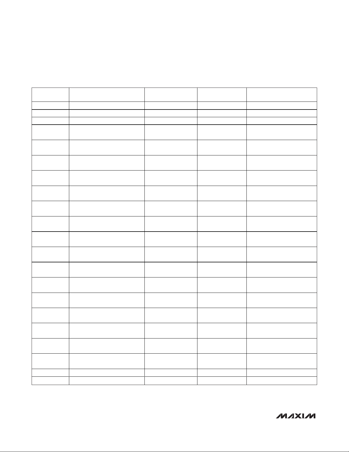
ABSOLUTE MAXIMUM RATINGS
ELECTRICAL CHARACTERISTICS
(V
AVDD
= V
DVDD
= 3.0V to 3.6V, VEN= 2V, V
RS_+
- V
RS_-
= 2V, V
RS_-
= 0V, TA= TJ= -40°C to +85°C, unless otherwise specified.
Typical values are at V
AVDD
= V
DVDD
= 3.3V, TA= +25°C.) (Note 2)
Stresses beyond those listed under “Absolute Maximum Ratings” may cause permanent damage to the device. These are stress ratings only, and functional
operation of the device at these or any other conditions beyond those indicated in the operational sections of the specifications is not implied. Exposure to
absolute maximum rating conditions for extended periods may affect device reliability.
Note 1: Package thermal resistances were obtained using the method described in JEDEC specification JESD51-7, using a four-
layer board. For detailed information on package thermal considerations, refer to www.maxim-ic.com/thermal-tutorial
.
AVDD, DVDD to AGND ............................................-0.3V to +4V
AVDD to DVDD......................................................-0.3V to +0.3V
AGND to DGND.....................................................-0.3V to +0.3V
AGND1 to DGND...................................................-0.3V to +0.3V
RS_+, RS_- to AGND................................................-0.3V to +6V
RS_C, A1/SCLE, A2/SDAE,
A3/CONTROL to AGND ......................-0.3V to (AVDD + 0.3V)
RESET, SMBALERT, ENOUT_ to AGND...................-0.3V to +6V
SCL, SDA to DGND ..................................................-0.3V to +4V
DACOUT_, EN, CLKIO, REFO to AGND.....-0.3V to (AVDD + 0.3V)
DACOUT_ Current ..............................................................10mA
SDA Current ........................................................-1mA to +50mA
Input/Output Current (all other pins) ...................................20mA
Continuous Power Dissipation (T
A
= +70°C)
36-Pin 6mm x 6mm TQFN
(derate 35.7mW/°C above +70°C).............................2857mW
Thermal Resistance (Note 1)
θ
JA
................................................................................28°C/W
θ
JC
..................................................................................1°C/W
Operating Temperature Range ...........................-40°C to +85°C
Junction Temperature......................................................+150°C
Storage Temperature Range .............................-65°C to +150°C
Lead Temperature (soldering, 10s) .................................+300°C
AVDD/DVDD Operating Voltage
Range
AVDD Undervoltage Lockout
(AVDD Rising)
AVDD Undervoltage Lockout
Hysteresis
AVDD and DVDD Total Supply
Current
OUTPUT-VOLTAGE SENSING
Voltage Regulation Accuracy
(2V Range)
Voltage Regulation Accuracy
(5.5V Range)
RS_+, RS_- Differential Mode
Range
RS_- to GND Differential Voltage -250 +250 mV
RS_+ Input Bias Current
RS_- Input Bias Current 2V or 5.5V range, V
PARAMETER SYMBOL CONDITIONS MIN TYP MAX UNITS
V
UVLO
V
UVLO-HYS
= V
V
RS_+
TA = +25°C, V
T
= -40°C to +85°C, V
A
= 0V
V
RS_-
TA = +25°C, V
T
= -40°C to +85°C, V
A
V
= 0V
RS_-
2V range, V
5.5V range, V
RS_-
= 0V 12 18.5 mA
= 1.0V, V
RS_+
RS_+
= 2.5V, V
RS_+
RS_+
= -0.25V to +2V -20 +20
RS_+
= -0.25V to +5.5V -20 +100
RS_+
= -0.25V to +0.25V -20 0 µA
RS_-
= 0V -4 +4 mV
RS_-
= 1.0V,
= 0V -11 +11 mV
RS_-
= 2.5V,
3.0 3.6 V
2.75 2.8 2.95 V
100 mV
-6 +6 mV
-16.5 +16.5 mV
0 5.5 V
µA
Page 3
MAX16064
±0.3% Accurate, Quad, Power-Supply Controller with
Active-Voltage Output Control and PMBus Interface
_______________________________________________________________________________________ 3
ELECTRICAL CHARACTERISTICS (continued)
(V
AVDD
= V
DVDD
= 3.0V to 3.6V, VEN= 2V, V
RS_+
- V
RS_-
= 2V, V
RS_-
= 0V, TA= TJ= -40°C to +85°C, unless otherwise specified.
Typical values are at V
AVDD
= V
DVDD
= 3.3V, TA= +25°C.) (Note 2)
INTERNAL TEMPERATURE SENSOR
Temperature Sensing Accuracy TA = 0°C to +85°C ±3 °C
INTERNAL OSCILLATOR
Frequency 7.6 8 8.4 MHz
ADC
Resolution 12 Bits
INTERNAL REFERENCE
Reference Voltage V
DAC
Resolution 12 Bits
Differential Nonlinearity DNL -2.5 +2.5 LSB
Maximum Output-Voltage Range No load
Capacitive Load 200 pF
Output-Voltage Slew Rate 0.35 V/µs
DAC Output Resistance 10 Ω
DAC Driving Capability DAC output > 100mV; output error < 25mV -1 +1 mA
DAC Output Leakage Current
CLKIO
Input Logic-Low Voltage 0.8 V
Input Logic-High Voltage 2.1 V
Input Bias Current V
Input Clock Duty Cycle 50 %
Output Low Voltage CLKIO in output mode, I
Output High Leakage V
CLKIO Pullup Voltage 3.6 V
CLKIO Input Frequency Range f
CLKIO Output Frequency 1 MHz
ENABLE INPUT (EN)
EN Falling Threshold Voltage V
EN Rising Threshold Voltage 1.175 1.23 1.281 V
EN Input Leakage Current -0.25 +0.25 µA
OUTPUTS (ENOUT_, RESET, SMBALERT)
Output Low Voltage V
Output Leakage V
PARAMETER SYMBOL CONDITIONS MIN TYP MAX UNITS
REF
EXT_CLK
EN_TH
OL
TA = +25°C 2.048 V
DAC output switch open,
V
I
V
_ = V
DACOUT
= 3.6V or 0V -1 +1 µA
CLKIO
= 3.6V -1 +1 µA
CLKIO
= 10mA 0.4 V
SINK
= V
AVDD
ENOUT_
DVDD
= 5V, 0V -1 +1 µA
V
REF -
1 LSB
or 0V
REF
= 1.1V, I
= 4mA 0.4 V
SINK
= 100µA 0.4 V
SINK
-250 +250 nA
100 1000 kHz
1.17 1.21 1.23 V
V
Page 4
MAX16064
±0.3% Accurate, Quad, Power-Supply Controller with
Active-Voltage Output Control and PMBus Interface
4 _______________________________________________________________________________________
ELECTRICAL CHARACTERISTICS (continued)
(V
AVDD
= V
DVDD
= 3.0V to 3.6V, VEN= 2V, V
RS_+
- V
RS_-
= 2V, V
RS_-
= 0V, TA= TJ= -40°C to +85°C, unless otherwise specified.
Typical values are at V
AVDD
= V
DVDD
= 3.3V, TA= +25°C.) (Note 2)
Note 2: 100% production tested at TA= +25°C. Limits over temperature are guaranteed by design.
Note 3: The MAX16064 supports SCL clock stretching.
PARAMETER SYMBOL CONDITIONS MIN TYP MAX UNITS
ADDRESS PINS (A1/SCLE, A2/SDAE, A3/CONTROL)
Input Logic-Low Voltage 0.3 V
Input Logic-Low Hysteresis 50 mV
V
Input Logic-High Voltage
AVDD
- 0.4
Input Logic-High Hysteresis 50 mV
Input Leakage Current -12 +12 µA
SMBus INTERFACE (SCL, SDA) (Note 3)
SCL, SDA Input Low Voltage V
SCL, SDA Input High Voltage V
SCL, SDA Input Leakage Current
(Per Pin)
Input Capacitance C
SCL, SDA Output Low Voltage V
Input voltage falling 0.8 V
IL
Input voltage rising 2.1 V
IH
Device powered or unpowered, V
IN
OL
to 3.6V, V
I
= 3mA 0.4 V
SINK
SCL
= V
SDA
= 0 or V
AVDD
AVDD
= 0V
-1 +1 µA
10 pF
SMBUS TIMING
Serial-Clock Frequency f
Bus Free Time Between STOP
and START Condition
START Condition Setup Time t
START Condition Hold Time t
STOP Condition Setup Time t
SU:STA
HD:STA
SU:STO
Clock Low Period t
Clock High Period t
Data Setup Time t
SU:DAT
Output Fall Time t
Data Hold Time t
HD:DAT
Pulse Width of Spike Suppressed t
SMBus Timeout t
TIMEOUT
SCL
t
BUF
LOW
HIGH
OF
SP
C
= 10pF to 400pF 300 ns
BUS
From 50% SCL falling to SDA change 300 ns
SMBCLK time low for reset 25 55 ms
10 100 kHz
4.7 µs
4.7 µs
4.0 µs
4.0 µs
4.7 µs
4.0 µs
250 ns
30 ns
OTHER TIMING PARAMETERS
PMBus Command Response
Time
Fault Response Time t
Recovery Time After Device
Reset
t
PMB_RSP
FAULT_RSP
t
RST_WAIT
300 µs
5ms
15 µs
V
Page 5
MAX16064
±0.3% Accurate, Quad, Power-Supply Controller with
Active-Voltage Output Control and PMBus Interface
_______________________________________________________________________________________ 5
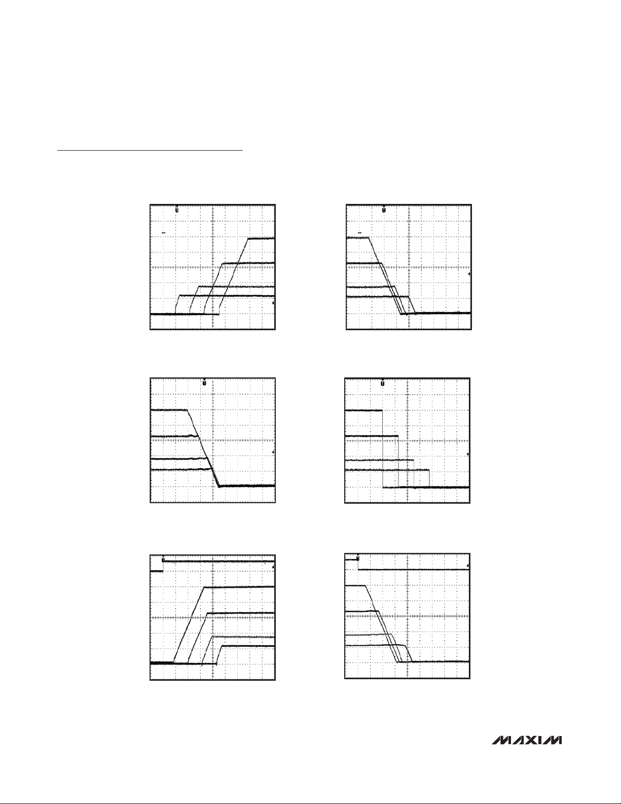
Typical Operating Characteristics
(V
AVDD
= V
DVDD
= 3.3V, TA= +25°C, unless otherwise noted.)
TOTAL SUPPLY CURRENT
vs. SUPPLY VOLTAGE
20
16
12
8
TOTAL SUPPLY CURRENT (mA)
4
0
2.6 3.6
TA = +85
V
AVDD
NC
= V
TA = +25NC
DVDD
UV_FAULT TO RESET RESPONSE
5V
3.3V
1ms/div
(V)
TA = -40NC
3.43.23.02.8
MAX16064 toc04
1.010
1.008
1.006
MAX16064 toc01
1.004
1.002
1.000
0.998
0.996
NORMALIZED EN THRESHOLD
0.994
0.992
0.990
-40 85
0.8
0.7
0.6
V
OUT0
2V/div
RESET
2V/div
0.5
0.4
0.3
0.2
ENOUT_ OUTPUT LOW VOLTAGE (V)
0.1
0
040
NORMALIZED EN THRESHOLD
vs. TEMPERATURE
NORMALIZED AT TA = +25NC
603510-15
TEMPERATURE (NC)
ENOUT_ OUTPUT LOW VOLTAGE
vs. SINK CURRENT
I
(mA)
SINK
NORMALIZED RESET TIMEOUT
1.10
1.08
MAX16064 toc02
1.06
1.04
1.02
1.00
0.98
0.96
NORMALIZED RESET TIMEOUT
0.94
0.92
0.90
0.5
0.4
0.3
MAX16064 toc05
0.2
0.1
-0.1
-0.2
-0.3
-0.4
POWER SUPPLIES OUTPUT ACCURACY (%)
35305 10 15 20 25
-0.5
PERIOD vs. TEMPERATURE
NORMALIZED AT TA = +25NC
-40 85
TEMPERATURE (NC)
603510-15
POWER SUPPLIES OUTPUT ACCURACY
vs. TEMPERATURE
VOUT2 = 1.8V
0
VOUT0 = 5V
VOUT1 = 3.3V
-40 85
TEMPERATURE (NC)
VOUT3 = 1.1V
603510-15
MAX16064 toc03
MAX16064 toc06
ENOUT_WITH AVDD = DVDD RISING
AVDD = DVDD RISING 3.3V/ms
200ms/div
MAX16064 toc07
AVDD = DVDD
1V/div
ENOUT1,2,3,4
2V/div
ENOUT_ WITH AVDD = DVDD FALLING
400Fs/div
MAX16064 toc08
AVDD = DVDD
1V/div
ENOUT1,2,3,4
2V/div
Page 6
MAX16064
±0.3% Accurate, Quad, Power-Supply Controller with
Active-Voltage Output Control and PMBus Interface
6 _______________________________________________________________________________________
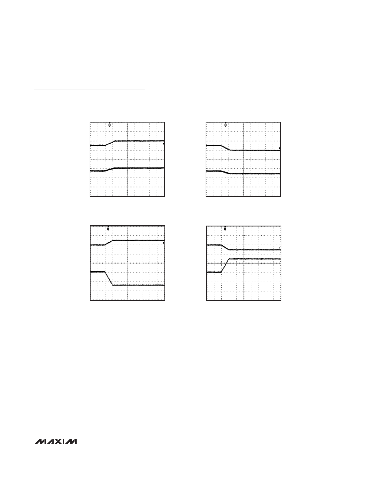
Typical Operating Characteristics (continued)
(V
AVDD
= V
DVDD
= 3.3V, TA= +25°C, unless otherwise noted.)
REFIN MODE SOFT-START
WITH SEQUENCING
2ms/div
REFIN MODE SOFT-STOP
WITH TRACKING
MAX16064 toc09
MAX16064 toc11
VOUT0 = 5V
VOUT1 = 3.3V
VOUT2 = 1.8V
VOUT3 = 1.1V
VOUT0 = 5V
VOUT1 = 3.3V
VOUT2 = 1.8V
VOUT3 = 1.1V
REFIN MODE SOFT-STOP
WITH SEQUENCING
2ms/div
MAX16064 toc10
REFIN MODE OPERATION OFF
WITH SEQUENCING
MAX16064 toc12
VOUT0 = 5V
VOUT1 = 3.3V
VOUT2 = 1.8V
VOUT3 = 1.1V
VOUT0 = 5V
VOUT1 = 3.3V
VOUT2 = 1.8V
VOUT3 = 1.1V
2ms/div
REFIN MODE SOFT-START FROM
A3 WITH SEQUENCING
2ms/div
MAX16064 toc13
REFIN MODE SOFT-STOP FROM
A3/CONTROL
5V/div
VOUT0 = 5V
VOUT1 = 3.3V
VOUT2 = 1.8V
VOUT3 = 1.1V
40ms/div
A3 WITH SEQUENCING
2ms/div
MAX16064 toc14
A3/CONTROL
5V/div
VOUT0 = 5V
VOUT1 = 3.3V
VOUT2 = 1.8V
VOUT3 = 1.1V
Page 7
MAX16064
±0.3% Accurate, Quad, Power-Supply Controller with
Active-Voltage Output Control and PMBus Interface
_______________________________________________________________________________________
7
Typical Operating Characteristics (continued)
(V
AVDD
= V
DVDD
= 3.3V, TA= +25°C, unless otherwise noted.)
REFIN MODE MARGINING
500mV HIGH AT 1mV/µs
400Fs/div
FB MODE MARGINING HIGH
FROM 5V TO 5.5V
5V
0.6V
MAX16064 toc15
MAX16064 toc17
5V
VOUT0
1V/div
0.6V
VDACOUT0
200mV/div
VOUT0
1V/div
4.5V
0.54V
0.6V
REFIN MODE MARGINING
500mV LOW AT 1mV/µs
400Fs/div
FB MODE MARGINING LOW
FROM 5V TO 4.5V
5V
MAX16064 toc16
VOUT0
1V/div
VDACOUT0
200mV/div
MAX16064 toc18
VOUT0
1V/div
VDACOUT0
200mV/div
VDACOUT0
200mV/div
400ms/div
400ms/div
Page 8
MAX16064
±0.3% Accurate, Quad, Power-Supply Controller with
Active-Voltage Output Control and PMBus Interface
8 _______________________________________________________________________________________
Pin Description
PIN NAME FUNCTION
1 RS2-
2 RS2+
3 RS3+
4 RS3-
5 RS3C Filter Capacitor for V
6EN
7 DACOUT1
8 AGND Analog Ground. Connect AGND to AGND1 and to DGND externally close to the device.
9 ENOUT0
10 ENOUT1
11 ENOUT2
12 ENOUT3
13 CLKIO
14 A1/SCLE
15 A2/SDAE
Differential Remote-Sense Input 2 Return of the DC-DC Output Voltage. Connect to the return terminal
at the load.
Differential Remote-Sense Input 2 of DC-DC Output Voltage. Connect to the load terminal where the
output must be regulated.
Differential Remote-Sense Input 3 of DC-DC Output Voltage. Connect to the load terminal where the
output must be regulated.
Differential Remote-Sense Input 3 Return of the DC-DC Output Voltage. Connect to the return terminal
at the load.
Amplifier 3. Connect a 1µF capacitor from RS3C to AGND.
SENSE
Enable Input. All ENOUT_ are deasserted when the voltage on EN is below 1.2V (typ). Used to turn
on/off the controlled power supplies in conjunction with the PMBus OPERATION command.
Analog Voltage Output of Internal 12-Bit DAC 1. Connect to TRIM, REFIN, or FB of a DC-DC module
or an LDO to adjust the power-supply output voltage. High impedance in shutdown.
On/Off Signal Output 0. Typically used to turn on/off a power supply. Controlled by the PMBus
OPERATION command or the sequencer. Can be configured as either an active-high or an active-low
open-drain output. See the ENOUT_ Operation section.
On/Off Signal Output 1. Typically used to turn on/off a power supply. Controlled by the PMBus
OPERATION command or the sequencer. Can be configured as either an active-high or an active-low
open-drain output. See the ENOUT_ Operation section.
On/Off Signal Output 2. Typically used to turn on/off a power supply. Controlled by the PMBus
OPERATION command or the sequencer. Can be configured as either an active-high or an active-low
open-drain output. See the ENOUT_ Operation section.
On/Off Signal Output 3. Typically used to turn on/off a power supply. Controlled by the PMBus
OPERATION command or the sequencer. Can be configured as either an active-high or an active-low
open-drain output. See the ENOUT_ Operation section.
Clock Input/Output. User-configurable clock input/output signal. The system controller can provide a
clock input to synchronize the time bases of multiple MAX16064 devices. Alternatively, a MAX16064
can provide a 1MHz output clock to other MAX16064s for synchronization. See the MFR_MODE (D1h)
section. When configured as an output, CLKIO is an open-drain output and a pullup resistor is
required.
Dual-Functioned MAX16064 Slave Address Identifier (LSB) and EEPROM I
MAX16064 Address Assignment and External EEPROM Interface sections.
Dual-Functioned MAX16064 Slave Address Identifier and EEPROM I
MAX16064 Address Assignment and External EEPROM Interface sections.
2
C Clock Output. See the
2
C Data Input/Output. See the
Dual-Functioned MAX16064 Slave Address Identifier (MSB) and Power-Supply On/Off Control Using
16 A3/CONTROL
17 RESET Active-Low, Open-Drain Reset Output
the MFR_MODE Command. See the MAX16064 Address Assignment and A3/CONTROL Operation
sections.
Page 9
MAX16064
±0.3% Accurate, Quad, Power-Supply Controller with
Active-Voltage Output Control and PMBus Interface
_______________________________________________________________________________________ 9
Pin Description (continued)
PIN NAME FUNCTION
18 SMBALERT Active-Low, Open-Drain Fault-Detection Interrupt Output
19 SCL SMBus Serial-Clock Input/Output
20 SDA SMBus Serial-Data Input/Output
21 DGND Digital Ground. Connect DGND to AGND and AGND1 externally close to the device.
22 DVDD Digital Power-Supply Input. Connect a 1µF capacitor from DVDD to DGND.
23 RSVD Reserved. Connect to DVDD externally.
24 DACOUT3
25 AGND1 Analog Ground. Connect to AGND and DGND externally close to the device.
26 AVDD Analog Power-Supply Input. Connect a 1µF capacitor from AVDD to AGND.
27 DACOUT2
28 RS1-
29 RS1+
30 RS1C Filter Capacitor for V
31 REFO Reference Output. Connect a 1µF capacitor from REFO to AGND.
32 RS0+
33 RS0C Filter Capacitor for V
34 RS0-
35 DACOUT0
36 RS2C Filter Capacitor for V
—EP
Analog Voltage Output of Internal 12-Bit DAC 3. Connect to TRIM, REFIN, or FB of a DC-DC module
or an LDO to adjust the power-supply output voltage. High impedance in shutdown.
Analog Voltage Output of Internal 12-Bit DAC 2. Connect to TRIM, REFIN, or FB of a DC-DC module
or an LDO to adjust the power-supply output voltage. High impedance in shutdown.
Differential Remote-Sense Input 1 Return of the DC-DC Output Voltage. Connect to the return terminal
at the load.
Differential Remote-Sense Input 1 of DC-DC Output Voltage. Connect to the load terminal where the
output must be regulated.
Amplifier 1. Connect a 1µF capacitor from RS1C to AGND.
SENSE
Differential Remote-Sense Input 0 of DC-DC Output Voltage. Connect to the load terminal where the
output must be regulated.
Amplifier 0. Connect a 1µF capacitor from RS0C to AGND.
SENSE
Differential Remote-Sense Input 0 Return of the DC-DC Output Voltage. Connect to the return terminal
at the load.
Analog Voltage Output of Internal 12-Bit DAC 0. Connect to TRIM, REFIN, or FB of a DC-DC module
or an LDO to adjust the power-supply output voltage. High impedance in shutdown.
Amplifier 2. Connect a 1µF capacitor from RS2C to AGND.
SENSE
Exposed Pad. Internally connected to AGND. Connect EP to the ground plane of the power supplies
for best temperature measurement performance.
Page 10
MAX16064
±0.3% Accurate, Quad, Power-Supply Controller with
Active-Voltage Output Control and PMBus Interface
10 ______________________________________________________________________________________
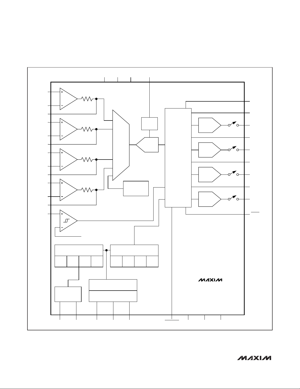
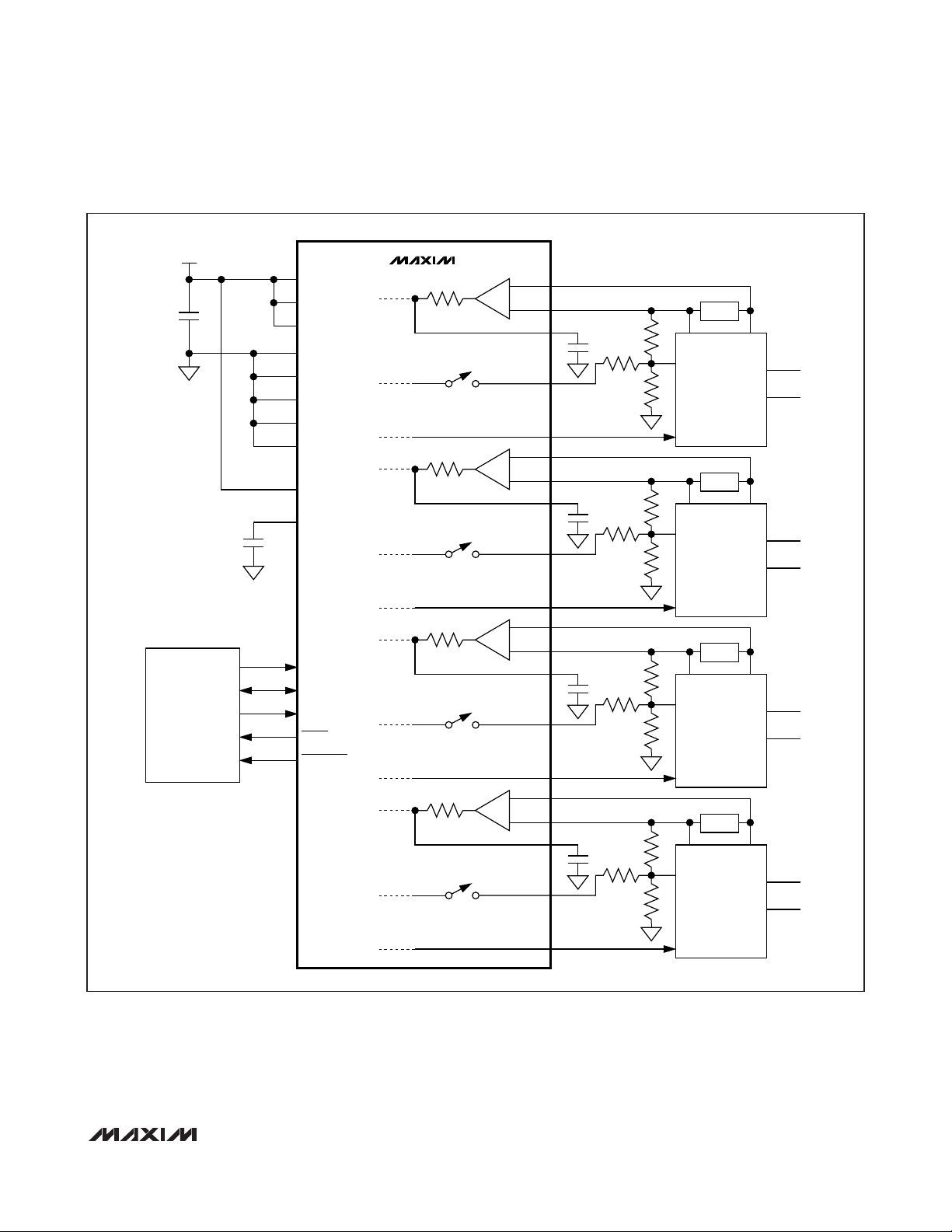
Figure 1. MAX16064 Functional Diagram
RS0+
RS0-
RS0C
RS1+
RS1-
RS1C
RS2+
RS2-
RS2C
RS3+
RS3-
RS3C
EN
VOLTAGE
SCALING
AND
MUX
RSVDDVDDAVDD
INTERNAL
TEMP
SENSOR
REFO
REF
12-BIT ADC
(SAR)
DIGITAL
COMPARATORS
AND
SEQUENCER
12-BIT VOUT
DAC 0
12-BIT VOUT
DAC 1
12-BIT VOUT
DAC 2
12-BIT VOUT
DAC 3
CLK0
ENOUT0
S0
DACOUT0
ENOUT1
S1
DACOUT1
ENOUT2
S2
DACOUT2
ENOUT3
S3
DACOUT3
RESET
1.2V
PMBus DEFAULT MEMORY
(EXTERNAL EEPROM)
PAGE
PAGE1PAGE2PAGE
0
EXTERNAL
EEPROM
INTERFACE
A1/SCLE A2/SDAE A3/CONTROL SCL SDA DGND AGND AGND1SMBALERT
3
I2C SMBus INTERFACE
PAGE
PMBus CONTROL
PMBus
OPERATING MEMORY
PAGE1PAGE2PAGE
0
3
MAX16064
Page 11
MAX16064
±0.3% Accurate, Quad, Power-Supply Controller with
Active-Voltage Output Control and PMBus Interface
______________________________________________________________________________________ 11
Detailed Description
The MAX16064 adds digital control functionality to four
power supplies. Using a closed-loop control system,
the MAX16064 can continuously adjust the power-supply output voltages to maintain ±0.3% output-voltage
accuracy. The MAX16064 can also be programmed to
sequence, track, and margin each power supply.
A PMBus-compliant interface bus provides access to
configuration parameters of the MAX16064, including
monitoring thresholds, sequence delays, soft-start and
soft-stop slew rates, output-voltage settings, an on-chip
temperature sensor, and more.
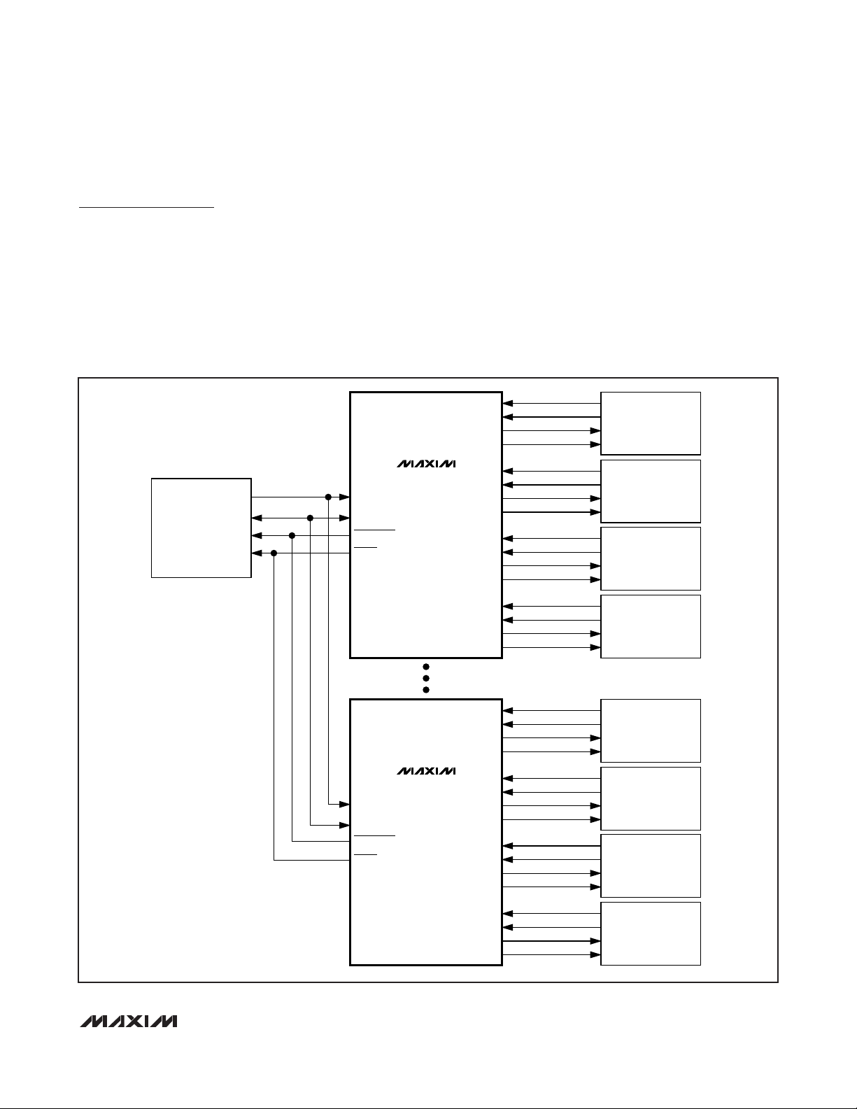
Up to 114 MAX16064s can reside on the same PMBus
bus, each controlling its own power supplies, under
commands from the PMBus system controller, as shown
in Figure 2. The MAX16064s can be placed close to the
power supplies they control so that all sensitive analog
traces are short and less susceptible to noise. The
power supplies can also be placed close to the load
where they provide the best transient response and lowest losses with short power plane runs.
MAX16064
RS0+ VO+
RS0- VO-
DACOUT0 FB
ENOUT0 EN
POWER
SUPPLY
0
RS1+ VO+
RS1- VO-
DACOUT1 FB
ENOUT1 EN
POWER
SUPPLY
1
RS2+ VO+
RS2- VO-
DACOUT2 FB
ENOUT2 EN
POWER
SUPPLY
2
RS3+ VO+
RS3- VO-
DACOUT3 FB
ENOUT3 EN
POWER
SUPPLY
3
SCL
SDA
IRQ
RST
SYSTEM
CONTROLLER
SCL
SDA
SMBALERT
RESET
MAX16064
RS0+ VO+
RS0- VO-
DACOUT0 FB
ENOUT0 EN
POWER
SUPPLY
(N-3)
RS1+ VO+
RS1- VO-
DACOUT1 FB
ENOUT1 EN
POWER
SUPPLY
(N-2)
RS2+ VO+
RS2- VO-
DACOUT2 FB
ENOUT2 EN
POWER
SUPPLY
(N-1)
RS3+ VO+
RS3- VO-
DACOUT3 FB
ENOUT3 EN
POWER
SUPPLY
(N)
SCL
SDA
SMBALERT
RESET
Figure 2. System Application Showing Multiple MAX16064s Controlling Power Supplies
Page 12

MAX16064
±0.3% Accurate, Quad, Power-Supply Controller with
Active-Voltage Output Control and PMBus Interface
12 ______________________________________________________________________________________
MAX16064 Operating Modes
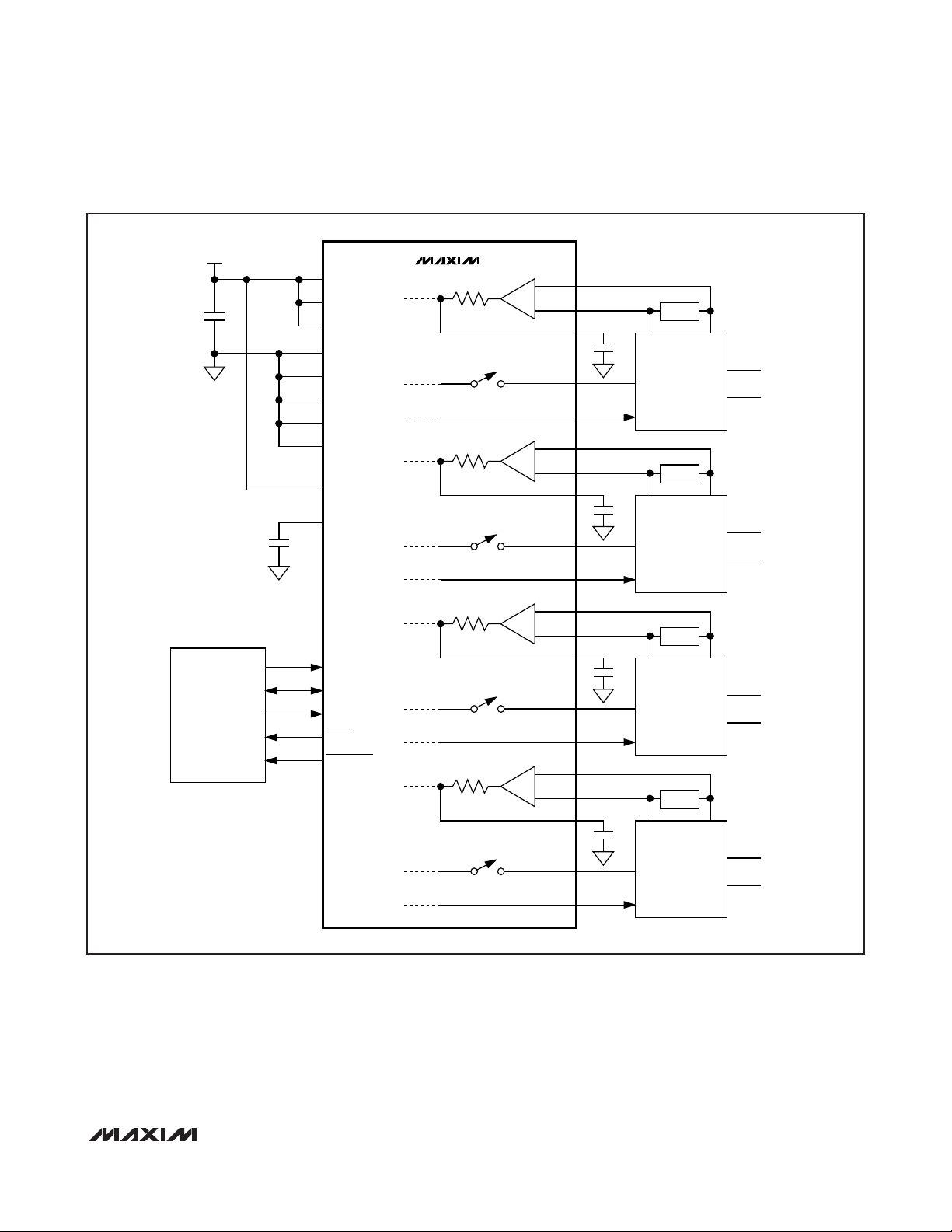
Reference Input (REFIN) Mode
Figure 3 shows how to connect a MAX16064 to the reference voltage input of a typical power supply, allowing
the MAX16064 to fully control the power-supply output
voltage. Connect a DACOUT_ of the MAX16064 to the
REFIN input of the power supply and connect the output-voltage terminals of the power supply to the RS_+
and RS_- sense inputs of the MAX16064. The sensed
voltage on RS_+ and RS_- is filtered by an internal
200Ω resistor and an external capacitor connected to
RS_C, and is digitized by a 12-bit ADC that uses an
accurate internal reference voltage.
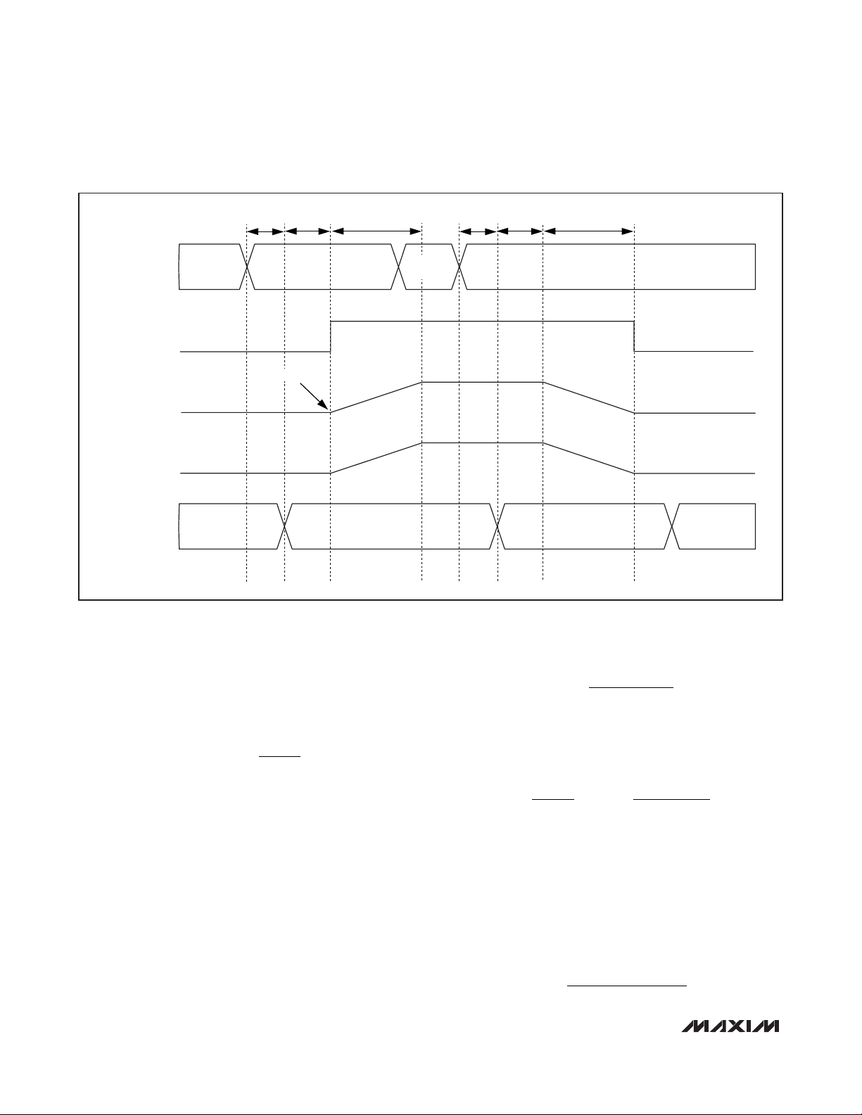
Normal operation begins as follows: upon receiving an
OPERATION ON command or a turn-on signal from
A3/CONTROL, the MAX16064 waits the programmed
t
ON_DELAY
time, then switches on the associated
ENOUT_ output and ramps up the power-supply output
voltage to its target VOUT_COMMAND value precisely
in the programmed t
ON_RISE
time. This facilitates easy
implementation of tracking of multiple output rails. On
reaching the target output voltage, the MAX16064 continuously monitors the power-supply output voltage
obtained at the RS_+ and RS_- inputs, and regulates it
to within ±0.3% by incrementing or decrementing the
DACOUT_ output 1 LSB (0.5mV) at a time. The
MAX16064 output-voltage correction rate is controlled
by MFR_MODE.1, VLTO, and DAC_ACT_CNT, as discussed in the
ADC Conversion, Monitoring, and AVOC
Adjustment Rates
section.
Once the requested target power-supply voltage is
reached, it can be margined up or down at a slew rate
programmed by the VOUT_TRANSITION_RATE parameter. To achieve this, the MAX16064 increments or
decrements the DACOUT_ output in a suitable number
of steps that depend on the programmed transition
rate. The number of steps is calculated from the
VOUT_SCALE_LOOP parameter, which must be set to
the ratio of the power-supply output voltage to the
power-supply reference voltage. This ratio is the same
as the voltage-divider ratio implemented on the power
supply from its output voltage node to the inverting
input of its error amplifier. This allows the MAX16064 to
correctly calculate the number of DACOUT steps and
voltage increments/decrements per step and thus
achieve the programmed rise time and transition time.
Since the reference voltage input is provided by the
MAX16064, the REFIN mode provides complete control
of the power supply in terms of soft-start, soft-stop, and
margining transitions.
Upon receiving an OPERATION OFF command or a
turn-off signal from A3/CONTROL, the MAX16064 waits
the programmed t
OFF_DELAY
time, ramps the output
voltage down to zero in the programmed t
OFF_FALL
time, then deasserts the ENOUT_ output. Each of the
four power-supply converters has its own set of delay
parameters, so sequencing is accomplished by loading
different delay times for each power supply.
Feedback (FB) Mode
Some power-supply converters do not provide a reference input. In these applications, the feedback node
can be used instead. Connect a DACOUT_ output of
the MAX16064 to the feedback node (FB) through a
resistor RFBas shown in Figure 5. In steady-state operation, the MAX16064 controls the power-supply voltage
as measured between RS_+ and RS_- to 0.3% accuracy by adjusting DACOUT_ 1 LSB at a time (0.5mV), up
and down as required. This mode of operation is
termed FB mode. Since the MAX16064 does not have
control over the power-supply error-amplifier reference
voltage, this mode relies on the power-supply soft-start
setting to implement the required soft-start time.
Upon receiving an OPERATION ON command or a
turn-on signal from A3/CONTROL, the MAX16064 waits
the programmed t
ON_DELAY
time, turns on the ENOUT_
output, causing the power supply to ramp up its output
voltage to its target value. The soft-start time taken by
the power supply to ramp from zero to its commanded
output voltage should be entered into the MAX16064
with the t
ON_RISE
parameter.
During t
ON_RISE
, the MAX16064 maintains DACOUT_ in
a high-impedance state by keeping the S_ switches
open. This allows the voltage at DACOUT_ to equal that
of the FB node of the power supply. At the end of the
t
ON_RISE
delay time, the internal DAC output voltage is
set to match the external voltage measured on
DACOUT_, and then the DACOUT_ switch S_ is closed.
The voltages on either side of the resistor RFBshould
be equal, or very close to equal. Under these conditions, little or no current flows into the FB node from
DACOUT_ and no perturbations are introduced to the
output voltage. From this point on, the MAX16064
adjusts the voltage at DACOUT_ to provide accurate
output-voltage control. In FB mode, the user must supply t
ON_DELAY
and t
ON_RISE
. If those parameters are
not set (the default values are zero), S_ closes prematurely and causes the supply voltage to overshoot or
undershoot.
Page 13
MAX16064
±0.3% Accurate, Quad, Power-Supply Controller with
Active-Voltage Output Control and PMBus Interface
______________________________________________________________________________________ 13
Figure 3. Typical System Application—REFIN Mode
3.3V
1µF
SYSTEM
CONTROLLER
IRQ
1µF
AVDD
DVDD
RSVD
AGND
AGND1
DGND
A1/SCLE
A2/SDAE
A3/CONTROL
REFO
SCL
SDA
EN
RESET
SMBALERT
MAX16064
200Ω
S0
200Ω
S1
200Ω
S2
200Ω
S3
RS0-
RS0+
RS0C
DACOUT0
ENOUT0
RS1-
RS1+
RS1C
DACOUT1
ENOUT1
RS2-
RS2+
RS2C
DACOUT2
ENOUT2
RS3-
RS3+
RS3C
DACOUT3
ENOUT3
LOAD
VO+ VO-
POWER
SUPPLY
REFIN
0
EN
LOAD
VO+ VO-
POWER
SUPPLY
REFIN
1
EN
LOAD
VO+ VO-
POWER
SUPPLY
REFIN
2
EN
LOAD
VO+ VO-
POWER
SUPPLY
REFIN
3
EN
VIN+
VIN-
VIN+
VIN-
VIN+
VIN-
VIN+
VIN-
Page 14
MAX16064
±0.3% Accurate, Quad, Power-Supply Controller with
Active-Voltage Output Control and PMBus Interface
14 ______________________________________________________________________________________
After receiving an OPERATION OFF command or a
turn-off signal from A3/CONTROL, the MAX16064 waits
the programmed t
OFF_DELAY
time, deasserts the
ENOUT_ output, and turns off the power supply.
For the FB mode, use the following formula to calculate
the value of RFB:
Where R1is the upper feedback divider resistor, ∆VOis
the required change in output voltage, and ∆V
DAC
is
the DACOUT output-voltage change that the user
allows. The recommended operating range for the
DACOUT_ voltage for power-supply output voltage
adjustment is between 30mV and 2V. Note that ∆V
DAC
is the difference between the steady-state power-supply FB node voltage, VFB, and the voltage limits on
DACOUT_. This is best illustrated with an example as
follows:
Consider an application involving a power supply with
VFB= 0.6V. Let the desired margining be ±10% for a
power-supply output voltage of 1V. For a power supply
with an upper voltage divider resistor R
1
= 10kΩ, RFBis
calculated as follows:
This value of RFBallows the MAX16064 to margin the
power-supply output voltage up by 10%. It is useful to
check the margin low condition by using the formula:
The effective margining range for the 57kΩ resistor
therefore turns out to be between +10% and -24.5%.
Note that the VOUT_TRANSITION_RATE parameter has
no effect on FB mode. The transition time for margining
in the FB mode of operation is a function of the update
rate (f
AVOC
), see the
MFR_DAC_ACT_CNT (E0h)
sec-
tion for the calculation of f
AVOC
. RFBand R1, and is
given by the following formula:
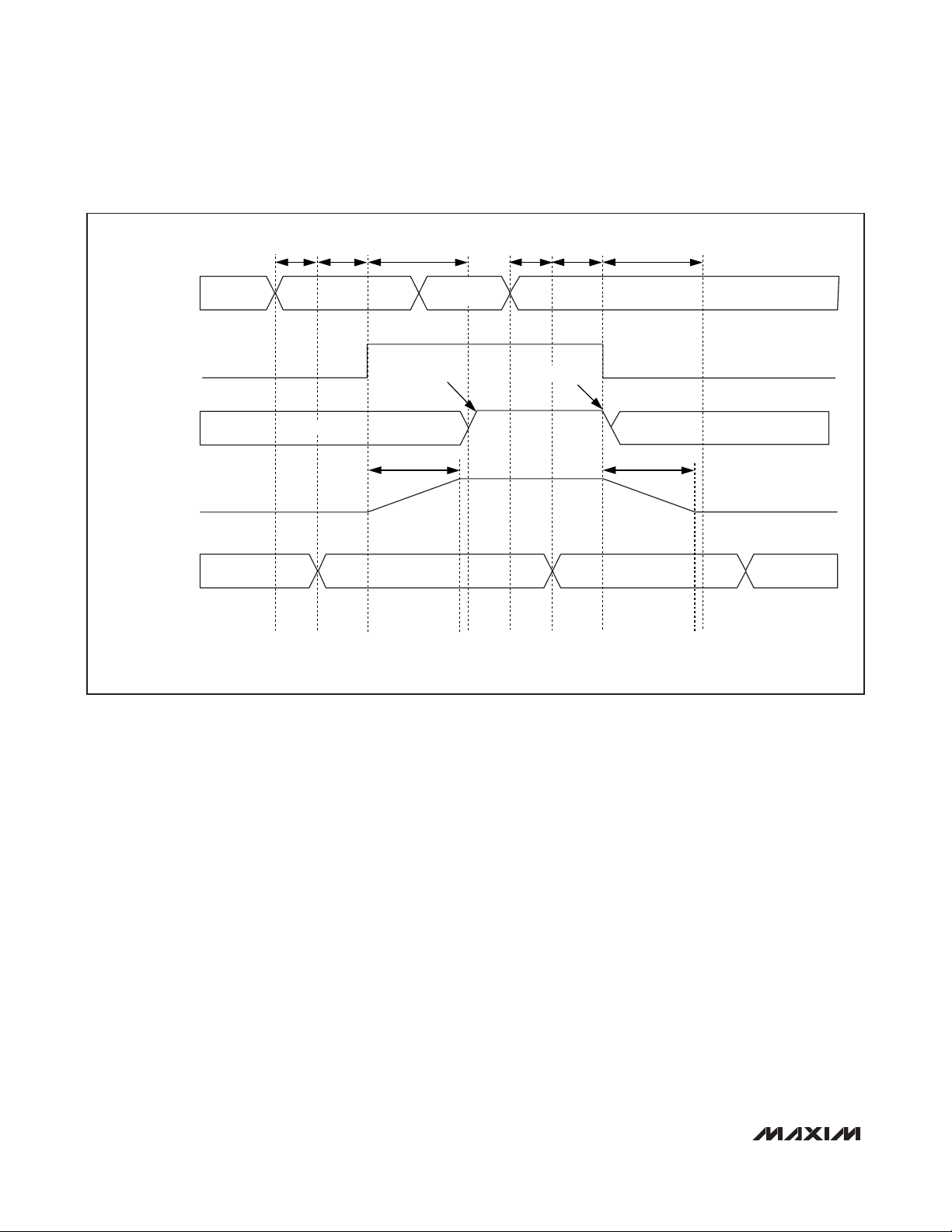
Figure 4. REFIN Mode Timing
t
PMB_RSPtON_DELAY
PMBus
ENOUT_
OPERATION
ON
IDLE IDLE
CLOSE S_
DAC OUTPUT
POWER-SUPPLY
V
OUT
POWER-SUPPLY
OPERATION
RR
=×
FB
V
∆
DAC
1
V
∆
O
t
ON_RISE
TURN-ON
t
PMB_RSPtOFF_DELAY
OPERATION
OFF
t
ON_FALL
TURN-OFF
−
VV
06 003
Rk
=× =
10
FB
(. . )
V
01
.
∆
V
∆
VR
=× = × =
O
DAC
1
R
FB
10
Ω
k
−
VV
20 06
(. . )
Ω
k
57
RxVx
t
FB
⎛
=
⎜
⎝
∆ 2000
FB O
fxR
AVOC
⎞
⎟
⎠
1
k
57ΩΩ
024
.55V
Page 15
MAX16064
±0.3% Accurate, Quad, Power-Supply Controller with
Active-Voltage Output Control and PMBus Interface
______________________________________________________________________________________ 15
Figure 5. Typical System Application—Feedback Mode
3.3V
1µF
1µF
AVDD
DVDD
RSVD
AGND
AGND1
DGND
A1/SCLE
A2/SDAE
A3/CONTROL
REFO
MAX16064
200Ω
S0
200Ω
S1
RS0-
RS0+
RS0C
DACOUT0
ENOUT0
RS1-
RS1+
RS1C
DACOUT1
LOAD
R1
VO+ VO-
FB
R
FB
R1
R
FB
POWER
SUPPLY
0
EN
LOAD
VO+ VO-
FB
POWER
SUPPLY
1
VIN+
VIN-
VIN+
VIN-
SCL
SDA
SYSTEM
CONTROLLER
IRQ
EN
RESET
SMBALERT
200Ω
S2
200Ω
S3
ENOUT1
RS2-
RS2+
RS2C
DACOUT2
ENOUT2
RS3-
RS3+
RS3C
DACOUT3
ENOUT3
EN
LOAD
R1
VO+ VO-
FB
R
FB
R1
R
FB
POWER
SUPPLY
2
EN
LOAD
VO+ VO-
FB
POWER
SUPPLY
3
EN
VIN+
VIN-
VIN+
VIN-
Page 16
MAX16064
±0.3% Accurate, Quad, Power-Supply Controller with
Active-Voltage Output Control and PMBus Interface
16 ______________________________________________________________________________________
Temperature Sensing
To obtain useful temperature readings, place the
MAX16064 in close proximity to the power supplies.
The on-chip temperature sensor on the MAX16064
senses the temperature of the die, which is related to
the exposed pad temperature of the MAX16064 by the
junction-to-case thermal resistance. The exposed pad
of the MAX16064 can connect to the heat dissipating
ground plane of the power supplies, and the power
supplies’ boards can be characterized to obtain the
relationship between the power supplies’ temperature
and temperature as measured by the MAX16064. This
information can be used to set overtemperature fault
settings in the MAX16064.
ADC Conversion, Monitoring,
and AVOC Adjustment Rates
Several timing parameters control the rate at which the
MAX16064 monitors voltages and temperatures and the
rate at which the MAX16064 adjusts the power-supply
output voltages. Each of the four voltage input channels
and the single temperature channel conversions are
performed round-robin fashion. If the input filter is
turned on by setting register MFR_MODE[1] to 0, then
four conversions are performed for each channel
instead of just one. A small programmable delay is
inserted in between each conversion, determined by
the MFR_VLTO register. This establishes the total conversion rate of the voltages and temperature. Smaller
values of MFR_VLTO results in a higher sampling rate,
and larger values of MFR_VLTO allow for more ADC
settling time.
The ADC conversion result registers are compared to
the fault threshold registers at a rate that is independent of the total conversion rate. The value of register
MFR_SAMPLE_RATE determines how frequently this
comparison occurs. Using higher fault comparison
rates increases glitch sensitivity, but slows the
response time of the MAX16064 to PMBus commands.
Using lower fault comparison rates makes the
MAX16064 less sensitive to power-supply output voltage glitches.
PMBus
OPERATION
ON
IDLEIDLE
t
PMB_RSPtON_DELAY
t
ON_RISE
t
PS_RISE
t
PS_FALL
t
PMB_RSPtOFF_DELAY
t
OFF_FALL
HIGH-Z
ENOUT_
DAC OUTPUT
POWER-SUPPLY
V
OUT
POWER-SUPPLY
OPERATION
IN FB MODE, t
PS_RISE
AND t
PS_FALL
ARE NOT CONTROLLED BY THE MAX16064 AND ARE DEPENDENT ON POWER-SUPPLY IMPLEMENTATION.
CLOSE S_
TURN-ON
TURN-OFF
OPEN S_
HIGH-Z
OPERATION
OFF
Figure 6. Feedback Mode Timing
Page 17

MAX16064
±0.3% Accurate, Quad, Power-Supply Controller with
Active-Voltage Output Control and PMBus Interface
______________________________________________________________________________________ 17
Finally, the AVOC system uses a separate control loop
rate that is related to the total ADC conversion rate. The
value of register MFR_DAC_ACT_CNT sets the number
of total ADC conversion cycles (one cycle is a complete
set of ADC conversions for 4 voltages and 1 temperature) that must occur before AVOC changes the DAC
output voltage. Smaller values of MFR_DAC_ACT_CNT
shorten the adjustment time. Larger values of
MFR_DAC_ACT_CNT adjust the output voltage at much
slower rates, reducing possible negative effects on the
power-supply control loop.
External EEPROM Interface
The MAX16064 can communicate with an EEPROM
attached to the A1/SCLE and A2/SDAE. The MAX16064
communicates to the EEPROM with an address byte of
1010 0000 for writing and 1010 0001 for reading. For
the data values of 2 bytes, the most significant byte is
stored in the lower address of the EEPROM, whereas
the least significant byte is stored in the higher address
of the EEPROM.
Upon reset, the MAX16064 tests for the presence of a
configuration EEPROM. It searches for the SIGNATURE
bytes in the attached EEPROM. If the SIGNATURE
bytes are present, it concludes that it has a valid configuration EEPROM and starts reading configuration
information from the attached EEPROM. If the slave
address (MFR_SET_ADDRESS) is a value other than
0x00, this overrides the slave address information previously set by the address A3:A1 pins.
Table 1b shows the contents and addresses of the configuration information expected by the MAX16064. This
information is for reference only. It is recommended to
use a properly configured, working MAX16064 to save
its state to the EEPROM and limit direct modifications to
as few fields as possible (such as the slave address).
Temperature and voltage values are stored in an internal representation, which is not the same as the format
used by the corresponding PMBus commands. For
details on the EEPROM internal representation, see
Conversion Rules (Table 1a).
For example, to store to the EEPROM PAGE 2
VOUT_COMMAND = 3.0V, m = 19995, b = 0, R = -1.
First calculate the PMBUS command value, which is
5998. If the voltage range is 2V, no conversion is
required. Hence write 17h to address 28 and 6Eh to
address 29. If the voltage range is 5.5V, the stored
EEPROM value = 5998/2.75 = 2181. So write 08h to
address 28 and write 85h to address 29.
Note that the conversion is automatically handled by
the MAX16064 when it stores and loads configuration
information.
Table 1a. Conversion Rules
READ (INTERNAL TO PMBus) WRITE (PMBus TO INTERNAL)
TEMPERATURE Subtract 3010 (decimal) from the PMBus value Add 3010 (decimal) to the PMBus value
VOLTAGE
No conversion in 2V mode;
multiply by 2.75 in 5.5V mode
No conversion in 2V mode;
divide by 2.75 in 5.5V mode
Table 1b. 16-Bit Words Stored in EEPROM
EEPROM
ADDRESS
NAME PAGE
PMBus COMMAND
NOTES
0 MFR_FAULT_REASON — 0E2h —
2 MFR_MODE — 0D1h
Must also match
MFR_TICK_RELOAD
4 TEMPERATURE_PEAK — 0D6h
Internal representation
(temperature)
6 MFR_FAULT_TEMP — 0E4h
Internal representation
(temperature)
8 MFR_VOUT_PEAK 0
10 MFR_VOUT_PEAK 1
12 MFR_VOUT_PEAK 2
14 MFR_VOUT_PEAK 3
0D4h
Internal representation
(voltage)
Page 18

MAX16064
±0.3% Accurate, Quad, Power-Supply Controller with
Active-Voltage Output Control and PMBus Interface
18 ______________________________________________________________________________________
Table 1b. 16-Bit Words Stored in EEPROM (continued)
EEPROM
ADDRESS
NAME PAGE
PMBus COMMAND
NOTES
16 MFR_FAULT_VOUT 0
18 MFR_FAULT_VOUT 1
20 MFR_FAULT_VOUT 2
22 MFR_FAULT_VOUT 3
0E3h
Internal representation
(voltage)
24 VOUT_COMMAND 0
26 VOUT_COMMAND 1
28 VOUT_COMMAND 2
30 VOUT_COMMAND 3
21h
Internal representation
(voltage)
32 TON_RISE 0
34 TON_RISE 1
36 TON_RISE 2
38 TON_RISE 3
61h —
40 TON_DELAY 0
42 TON_DELAY 1
44 TON_DELAY 2
46 TON_DELAY 3
60h —
48 VOUT_MARGIN_HIGH 0
50 VOUT_MARGIN_HIGH 1
52 VOUT_MARGIN_HIGH 2
54 VOUT_MARGIN_HIGH 3
25h
Internal representation
(voltage)
56 VOUT_MARGIN_LOW 0
58 VOUT_MARGIN_LOW 1
60 VOUT_MARGIN_LOW 2
62 VOUT_MARGIN_LOW 3
26h
Internal representation
(voltage)
64 TOFF_FALL 0
66 TOFF_FALL 1
68 TOFF_FALL 2
70 TOFF_FALL 3
65h —
72 OT_FAULT_LIMIT — 4Fh
Internal representation
74 MFR_SAMPLE_RATE — 0D3h —
76–87 Reserved (set to 0) — — —
88 MFR_FAULT_RESPONSE 0
90 MFR_FAULT_RESPONSE 1
92 MFR_FAULT_RESPONSE 2
94 MFR_FAULT_RESPONSE 3
0D9h —
96 MFR_FAULT_RETRY 0
98 MFR_FAULT_RETRY 1
100 MFR_FAULT_RETRY 2
102 MFR_FAULT_RETRY 3
0DAh —
Page 19

MAX16064
±0.3% Accurate, Quad, Power-Supply Controller with
Active-Voltage Output Control and PMBus Interface
______________________________________________________________________________________ 19
Table 1b. 16-Bit Words Stored in EEPROM (continued)
EEPROM
ADDRESS
NAME PAGE
PMBus COMMAND
NOTES
104–115 MFR_DATE — 9Dh —
116 MFR_STATUS_WORD — 0D8h Set to 0
118 WRITE_PROTECT — 10h —
120 ON_OFF_CONFIG 0
122 ON_OFF_CONFIG 1
124 ON_OFF_CONFIG 2
126 ON_OFF_CONFIG 3
02h —
128 VOUT_SCALE_LOOP 0
130 VOUT_SCALE_LOOP 1
132 VOUT_SCALE_LOOP 2
134 VOUT_SCALE_LOOP 3
29h —
136 OT_WARN_LIMIT — 51h
Internal representation
(temperature)
138 Reserved (set to 0) — — —
140 MFR_SET_ADDRESS — 0DBh
Low byte: I
2
C address,
high byte: reserved
142 Reserved (set to 0) — — —
144 TOFF_DELAY 0
146 TOFF_DELAY 1
148 TOFF_DELAY 2
150 TOFF_DELAY 3
64h —
152 VOUT_TRANSITION_RATE 0
154 VOUT_TRANSITION_RATE 1
156 VOUT_TRANSITION_RATE 2
158 VOUT_TRANSITION_RATE 3
27h —
160–175 Reserved (set to 0) 0 — —
176 MFR_MODE_OUTPUT 0
178 MFR_MODE_OUTPUT 1
180 MFR_MODE_OUTPUT 2
182 MFR_MODE_OUTPUT 3
0DEh —
184–199 Reserved (set to 0) — — —
200 MFR_RESET_DELAY — 0DDh —
202 MFR_RESET_OUTPUT — 0E1h —
204 Reserved (set to 0) — — —
206 MFR_TICK_RELOAD — 0D1h —
208 MFR_STATUS_WORD 0
210 MFR_STATUS_WORD 1
212 MFR_STATUS_WORD 2
214 MFR_STATUS_WORD 3
0D8h Set to 0
Page 20
MAX16064
±0.3% Accurate, Quad, Power-Supply Controller with
Active-Voltage Output Control and PMBus Interface
20 ______________________________________________________________________________________
Table 1b. 16-Bit Words Stored in EEPROM (continued)
EEPROM
ADDRESS
NAME PAGE
PMBus COMMAND
NOTES
216–237 MFR_LOCATION — 9Ch —
238–255 MFR_SERIAL — 9Eh —
256–297 MFR_USERDATA_00 — 0B0h —
298 VOUT_OV_FAULT_LIMIT 0 40h
Internal representation
(voltage)
300 VOUT_UV_FAULT_LIMIT 0 44h
Internal representation
(voltage)
302 VOUT_OV_WARN_LIMIT 0 42h
Internal representation
(voltage)
304 VOUT_UV_WARN_LIMIT 0 43h
Internal representation
(voltage)
306 VOUT_OV_FAULT_LIMIT 1 40h
Internal representation
(voltage)
308 VOUT_UV_FAULT_LIMIT 1 44h
Internal representation
(voltage)
310 VOUT_OV_WARN_LIMIT 1 42h
Internal representation
(voltage)
312 VOUT_UV_WARN_LIMIT 1 43h
Internal representation
(voltage)
314 VOUT_OV_FAULT_LIMIT 2 40h
Internal representation
(voltage)
316 VOUT_UV_FAULT_LIMIT 2 44h
Internal representation
(voltage)
318 VOUT_OV_WARN_LIMIT 2 42h
Internal representation
(voltage)
320 VOUT_UV_WARN_LIMIT 2 43h
Internal representation
(voltage)
322 VOUT_OV_FAULT_LIMIT 3 40h
Internal representation
(voltage)
324 VOUT_UV_FAULT_LIMIT 3 44h
Internal representation
(voltage)
326 VOUT_OV_WARN_LIMIT 3 42h
Internal representation
(voltage)
328 VOUT_UV_WARN_LIMIT 3 43h
Internal representation
(voltage)
330–509 Unused (set to 0) — — —
510 SIGNATURE (set to 4432h) — N/A —
Page 21

MAX16064
±0.3% Accurate, Quad, Power-Supply Controller with
Active-Voltage Output Control and PMBus Interface
______________________________________________________________________________________ 21
Figure 7 shows how the MAX16064 interfaces to an
external serial EEPROM using the A1/SCLE and
A2/SDAE in applications where a master controller
does not exist or is not required. Using the GUI, the
user can select each MAX16064 device and configure
all the required output-voltage settings and sequencing/tracking information. Once the configuration is complete, the results can be saved to the external EEPROM
by using the STORE_DEFAULT_ALL command and
configuration restored on the MAX16064 power-on
reset. The EEPROM can also be preprogrammed prior
to board assembly in the manufacturing environment.
A3/CONTROL can be used as a control signal to turn
on/off the power supply in a similar fashion as the
OPERATION command.
Use a serial EEPROM IC with a minimum of 4kb of storage to ensure proper device operation.
MAX16064 Operation
On power-up reset, the MAX16064 goes through an initialization process as shown in Figure 8.
After initialization, the MAX16064 monitors the PMBus and
executes the PMBus commands accordingly. In addition,
if the power supply has been commanded to turn on, the
MAX16064 also monitors the power-supply output voltage
and temperature at the MFR_SAMPLE_RATE. The
PMBus system controller can monitor the power-supply
health by issuing various inquiries and status commands to the MAX16064.
RESET
Output Operation
RESET is an active-low, open-drain output that is low when
the device is powering on. RESET is assigned to one of
the power supplies using the MFR_RESET_OUTPUT
command. When that power-supply output is at the target
voltage, RESET goes high after the reset timeout period
(see Figure 9). The reset timeout period (tRP) is set by the
MFR_RESET_DELAY command.
The MFR_RESET_OUTPUT value defines which powersupply output affects RESET. If MFR_RESET_OUTPUT is
set to 0, 1, 2, or 3, then RESET goes high tRPafter that
output has reached its target value. If MFR_RESET_OUTPUT is any other value, RESET is permanently low.
If the power-supply output selected by
MFR_RESET_OUTPUT is later disabled for any reason
(either due to a fault condition, or an OPERATION OFF
command), then RESET goes low immediately. To
enable faults on any power supply to cause RESET to
go low, set the MFR_MODE_OUTPUT.GLOBALFAULTS
bit to a 1 for all the supplies.
RESET requires an external pullup resistor.
33kΩ33kΩ
V
CC
1µF
1µF
VO+ VO-
1µF
DVDD
AVDD
3.3V
RSVD
EEPROM
24LCXX
SYSTEM
CONTROLLER
DGND
MAX16064
A1/SCLE
A2/SDAE
A3/CONTROL
SCL
SDA
RESET
SMBALERT
POWER
SUPPLY
A1
A2
A3
SCL
SDA
GND
IRQ
AGND
RS_RS_+
RS_C
DACOUT_
REFIN
VIN+
VIN-
REFO
ENOUT_
EN
LOAD
Figure 7. Typical System Application with External EEPROM
Page 22

MAX16064
±0.3% Accurate, Quad, Power-Supply Controller with
Active-Voltage Output Control and PMBus Interface
22 ______________________________________________________________________________________
SMBALERT
Output Operation
SMBALERT is an optional interrupt signal defined in
Appendix A of the SMBus specification. The MAX16064
provides an output SMBALERT as this interrupt signal.
SMBALERT is an active-low, open-drain output and it
asserts to signal the PMBus master if any of the voltage
or temperature fault has occurred. Typically,
SMBALERT is connected to all other SMBALERT opendrain signals in the system, creating a wired-OR function with all SMBALERT outputs. When the master is
interrupted by its SMBALERT input, it stops or finishes
the current bus transfer and places an alert response
address (ARA) on the bus. The slave that pulled the
SMBALERT signal low acknowledges the ARA and
places its own address on the bus, identifying itself to
the master as the slave that caused the interrupt.
SMBALERT deasserts when the MAX16064 responds to
the ARA. SMBALERT deasserts when all the fault conditions are removed. SMBALERT is also cleared by the
CLEAR_FAULTS command.
ENOUT_ Operation
When power is applied, all ENOUT_ are held low. Upon
receiving a command to turn on the power supply,
ENOUT_ goes high. The polarity can be changed by
the ENOUT_POL bit of the MFR_MODE_OUTPUT command. Setting the bit to a 1 makes the ENOUT_ active
low. If the bit in the external EEPROM is set to 1, upon
power-up, the ENOUT_ is held low until the bit is copied
from the EEPROM to the on-chip register at which time
the ENOUT_ goes high. Upon receiving a command to
turn on the power supply, ENOUT_ goes low. It takes
1.60ms (typ) to copy the configuration bits from the
EEPROM to the on-chip registers.
EN Operation
The MAX16064 includes an enable input (EN) that controls all ENOUT_ signals in conjunction with the
MFR_MODE command. Unless MFR_MODE.IGNORE_EN
is set, a below-threshold level on EN prevents any
ENOUT_ from turning on. Additionally, if the voltage at
EN falls below the 1.2V (typ) threshold during
OPERATION ON, the MAX16064 follows the fault action
in MFR_FAULT_RESPONSE.EN. Figure 9 shows a typical sequencing with MFR_MODE.IGNORE_EN = 0.
RESET
INITIALIZE
INTERNAL
REGISTERS
SET PMBus
ADDRESS
ACCORDING TO
A3:A1
VALID
EEPROM?
RESTORE
CONFIGURATION
FROM EEPROM
INTERNAL
REFERENCE
STABLE?
ENABLE PMBus
COMMUNICATION
PMBus
COMMAND?
Y
N
Y
Y
N
N
EXECUTE PMBus
COMMAND
ASSERT
SMBALERT
Figure 8. MAX16064 Initialization
Table 2. ENOUT_ Active State
ENOUT_
DEFAULT
STARTUP
STATE
MFR_MODE_OUTPUT.
ENOUT_POL
ENOUT_ ACTIVE
STATE
Low 0 Active high
Low 1 Active low
Page 23

MAX16064
±0.3% Accurate, Quad, Power-Supply Controller with
Active-Voltage Output Control and PMBus Interface
______________________________________________________________________________________ 23
MAX16064 Address Assignment
The MAX16064 picks a slave address in one of the two
ways described below:
1) Hardwired by A3:A2:A1.
2) Restored from EEPROM at power-on.
Address assignment order is shown in Figure 10.
The MAX16064 reads A3:A2:A1 address pins upon
device reset and determines its address according to
Table 3.
RESET
t
ON0
t
RP
t
OFF0
t
ON1
t
OFF1
t
OFF2
t
OFF3
t
ON2
t
ON3
ENOUT3
ENOUT2
ENOUT1
ENOUT0
EN
NOTE: MFR_RESET_OUTPUT = 3
Figure 9. MAX16064 Typical Sequencing Timing
Table 3. MAX16064 A3:A1 Slave Address Assignment
A3/CONTROL A2/SDAE A1/SCLE ADDRESS (BITS 7–1)
L L L 40h
LLZ 01h*
LZL 02h
LZZ 03h
ZLL 04h
ZLZ 05h
ZZL 06h
ZZZ 07h
L L H 09h
LZH 0Bh
ZLH 0Dh
Page 24

MAX16064
±0.3% Accurate, Quad, Power-Supply Controller with
Active-Voltage Output Control and PMBus Interface
24 ______________________________________________________________________________________
The hardwired address pins give 33= 27 address
options. For example, to configure the MAX16064 to
have a slave address of 010 0101 (25h), set A3:A2:A1
= H:L:Z. The MAX16064 also responds to the broadcast address (00h).
If an EEPROM with valid SIGNATURE bytes is attached
to the MAX16064, the MAX16064 tries to restore its
slave address from the EEPROM. This overrides the
address set by the address pins. This gives a total of
128 possible slave addresses. Note that there are 14
reserved addresses that are restricted by the PMBus
specification and may not be used in PMBus systems.
If the address bit 7 from the EEPROM is set to 1, this is
an invalid address and the MAX16064 continues using
the address set by the address pins. When an
EEPROM is attached to A2/SDAE and A1/SCLE, these
pins assume either a logic-high or a logic-low level,
therefore, the resulting number of possible addresses
set by the A3:A2:A1 pins in this scenario is 23= 8.
In addition, for the MAX16064 with an EEPROM
attached, the system controller can change the
MAX16064 slave address by sending the new address
with the MFR_SET_ADDRESS command. However, the
new address is not immediately effective. The new
address must be stored to the EEPROM first using the
STORE_DEFAULT_ALL command. Then, the
MAX16064 power must be cycled to start the address
assignment procedure and recalls the new address
from the EEPROM.
A3/CONTROL Operation
The A3/CONTROL input is utilized in combination with
the A2 and A1 inputs to set the PMBus address when
power is applied to the device. After the PMBus
address detection, the A3/CONTROL input functions as
the PMBus CONTROL input.
The ON_OFF_CONFIG command determines whether
the A3/CONTROL input affects the on/off behavior of the
power supply. When A3/CONTROL is enabled by the
ON_OFF_CONFIG command, a transition of A3/CONTROL from low to high turns the power supply on, as if
the MAX16064 has received an OPERATION ON
command. A transition of A3/CONTROL from high to low
initiates a soft-off to the power supply, as if the
MAX16064 has received an OPERATION OFF command (soft-off, with sequencing). The MAX16064 still
responds to the PMBus OPERATION command while
A3/CONTROL is enabled. To detect the A3/CONTROL
input, the A3/CONTROL signal pulse width has to satisfy the t
A3_LOW
and t
A3_HIGH
requirements to be detect-
ed. See the
ON_OFF_CONFIG (02h)
section and Table
6 for more information.
Table 3. MAX16064 A3:A1 Slave Address Assignment (continued)
A3/CONTROL A2/SDAE A1/SCLE ADDRESS (BITS 7–1)
ZZH 0Fh
L H L 12h
LHZ 13h
ZHL 16h
ZHZ 17h
L H H 1Bh
ZHH 1Fh
H L L 24h
HLZ 25h
HZL 26h
HZZ 27h
HLH 2Dh
HZH 2Fh
H H L 36h
HHZ 37h
H H H 3Fh
*
The shaded addresses are not available if external EEPROM is attached.
Page 25

MAX16064
±0.3% Accurate, Quad, Power-Supply Controller with
Active-Voltage Output Control and PMBus Interface
______________________________________________________________________________________ 25
Figure 10. MAX16064 Address Assignment
SET SLAVE
POWER ON
POWER OFF
ADDRESS
ACCORDING TO
A3:A1
VALID EEPROM
AND BIT7 STORED
ADDRESS IN EEPROM
IS NOT 1?
N
MFR_SET_ADDR?
N
SAVE TO
EEPROM?
Y
Y
Y
RESTORE SLAVE
ADDRESS FROM
EEPROM
SLAVE ADDRESS
UNCHANGED.
STORE NEW ADDRESS
TEMPORARILY.
SAVE NEW
ADDRESS TO
EEPROM
N
Page 26

MAX16064
±0.3% Accurate, Quad, Power-Supply Controller with
Active-Voltage Output Control and PMBus Interface
26 ______________________________________________________________________________________
The dual functionality of A3/CONTROL of the
MAX16064 requires that the system enable signal be
isolated from A3 until the address setting has been
read and latched by the MAX16064. Figure 11 shows
one implementation for the three possible states of the
A3/CONTROL setting. In each case, the system enable
signal (MAX16064_EN) is applied to the input of a
three-state buffer whose output is kept in the highimpedance state by a control input signal (HIZ_EN) for
a time period during which the MAX16064 reads and
latches the A3/CONTROL address setting. After this
period, the control signal HIZ_EN goes low and allows
the system enable signal to be applied to the
MAX16064 A3/CONTROL pin. After a t
A3_LOW
, the
MAX16064_EN signal transitions from low to high and
causes the MAX16064s to commence power-supply
startup operations.
PMBus Digital Interface
From a software perspective, the MAX16064 appears
as a PMBus device capable of executing a subset of
PMBus commands. A PMBus 1.0-compliant device
uses the SMBus version 1.1 for transport protocol and
responds to the SMBus slave address. In this data
sheet, the term SMBus is used to refer to the electrical
characteristics of the PMBus communication using the
SMBus physical layer. The term PMBus is used to refer
to the PMBus command protocol.
The MAX16064 employs five standard SMBus protocols
(Write Word, Read Word, Write Byte, Read Byte, and
Send Byte (see Figures 12–15)) to program output voltage and warning/faults thresholds, read monitored
data, and provide access to all manufacturer-specific
commands.
1µF
A3
A2
A1
REFO
AVDD
REFO
HIZ_EN
MAX16064_EN
HIZ_EN PLACES U1, U2, AND U3 OUTPUTS IN HIGH-IMPEDANCE STATE WHEN ASSERTED.
U1, U2, AND U3 ARE NOT NECESSARY IF AN EEPROM IS ATTACHED TO A1/SCLE
AND A2/SDAE. A1/SCLE, A2/SDAE ARE EITHER PULLED UP OR PULLED DOWN WITH
33kΩ WHEN CONNECTED TO AN EEPROM.
A3/CONTROL
MAX16064_UVLO
t
RST_WAIT
t
A3_LOW
3.3V
33kΩ
MAX16064_EN
HIZ_EN
U1
33kΩ
MAX16064
1µF
A3
A2
A1
REFO
U2
MAX16064
1µF
A3
A2
A1
REFO
U3
MAX16064
Figure 11. Application Diagram with A3/CONTROL as Both Address and On/Off Control Signal
Page 27

MAX16064
±0.3% Accurate, Quad, Power-Supply Controller with
Active-Voltage Output Control and PMBus Interface
______________________________________________________________________________________ 27
The MAX16064 supports the group command. The
group command is used to send commands to more
than one PMBus device. It is not required that all the
devices receive the same command. However, no
more than one command can be sent to any one
device in one group command packet. The group
command must not be used with commands that
require receiving devices to respond with data, such
as the STATUS_BYTE command. When the
MAX16064 receives a command through this protocol, it immediately begins execution of the
received command after detecting the STOP condition.
The MAX16064 supports the PAGE command and uses
it to select which individual channel to access.
When the data word is transmitted, the lower order byte
is sent first and the higher order byte is sent last. Within
any byte, the most significant bit (MSB) is sent first and
the least significant bit (LSB) is sent last.
The MAX16064 SMBus interface supports Packet Error
Checking (PEC). See the
MFR_MODE (D1h)
section.
ADDR
SLAVE ADDRESS COMMAND BYTE:
SELECTS TO WHICH
COMMAND PARAMETER
TO WRITE
DATA BYTE: DATA FOR THE COMMAND
SET BY THE COMMAND BYTE
WRITE BYTE FORMAT
SW
PA A A
7 BITS
COMMAND
8 BITS
DATA
8 BITS
ADDR
SLAVE ADDRESS COMMAND BYTE:
SELECTS FROM WHICH
COMMAND PARAMETER
TO READ
DATA BYTE: DATA FOR THE COMMAND
SET BY THE COMMAND BYTE
READ BYTE FORMAT
SSRW
PA R AA NA
7 BITS
ADDR
SLAVE ADDRESS:
REPEATED DUE TO
CHANGE IN DATA-FLOW
DIRECTION
7 BITS
COMMAND
8 BITS
DATA
8 BITS
ADDR
SLAVE ADDRESS COMMAND BYTE:
SELECTS TO WHICH
COMMAND PARAMETER
TO WRITE
DATA BYTE: DATA FOR THE COMMAND SET BY THE
COMMAND BYTE
WRITE WORD FORMAT
SW
PA A A
7 BITS
COMMAND
8 BITS
DATA0
8 BITS
ADATA1
8 BITS
ADDR
SLAVE ADDRESS COMMAND BYTE: SEND
COMMAND WITH NO DATA
SEND BYTE FORMAT
SW
S = START CONDITION
SR = REPEATED START CONDITION
P = STOP CONDITION
= SLAVE TRANSMISSION
PA A
7 BITS
COMMAND
8 BITS
ADDR
SLAVE ADDRESS COMMAND BYTE:
SELECTS FROM WHICH
COMMAND PARAMETER
TO READ
DATA BYTE: DATA FOR THE COMMAND SET BY THE
COMMAND BYTE
READ WORD FORMAT
SSRW
PA R AA A
7 BITS
ADDR
SLAVE ADDRESS:
REPEATED DUE TO
CHANGE IN DATA-FLOW
DIRECTION
7 BITS
COMMAND
8 BITS
DATA0
8 BITS
NADATA1
8 BITS
Figure 12. SMBus Protocols
Page 28

MAX16064
±0.3% Accurate, Quad, Power-Supply Controller with
Active-Voltage Output Control and PMBus Interface
28 ______________________________________________________________________________________
Figure 13. SMBus Group Command Protocol
SWA A A
SLAVE ADDRESS OF
DEVICE 1
SR W A A
SLAVE ADDRESS OF
DEVICE 2
SR W A A A
SLAVE ADDRESS OF
DEVICE 3
SR W
SLAVE ADDRESS OF
DEVICE n
ADDR1
7 BITS
ADDR2
7 BITS
ADDR3
7 BITS
ADDRn
7 BITS
CMD1
8 BITS
COMMAND BYTE FOR
DEVICE 1
CMD2
8 BITS
COMMAND BYTE FOR
DEVICE 2
CMD3
8 BITS
COMMAND BYTE FOR
DEVICE 3
CMDn
8 BITS
COMMAND BYTE FOR
DEVICE n: NO DATA BYTE
DATA0
8 BITS
DATA BYTES FOR DEVICE 1
8 BITS
DATA BYTES FOR DEVICE 2
DATA0
8 BITS
DATA BYTES FOR DEVICE 3
PA A
ADATA1
8 BITS
ADATA
ADATA1
8 BITS
S = START CONDITION
SR = REPEATED START CONDITION
P = STOP CONDITION
= SLAVE TRANSMISSION
Page 29

MAX16064
±0.3% Accurate, Quad, Power-Supply Controller with
Active-Voltage Output Control and PMBus Interface
______________________________________________________________________________________ 29
Figure 14. SMBus Protocols with PEC
WRITE BYTE FORMAT
S ADDR W A COMMAND A
7 BITS 8 BITS
SLAVE
ADDRESS
READ BYTE FORMAT
S ADDR W A COMMAND A
7 BITS 8 BITS
SLAVE
ADDRESS
WRITE WORD FORMAT
S ADDR W A COMMAND A
7 BITS 8 BITS
READ WORD FORMAT
S ADDR W A COMMAND A
7 BITS 8 BITS
SLAVE
ADDRESS
COMMAND BYTE:
SELECTS TO WHICH
COMMAND PARAMETER
TO WRITE
COMMAND BYTE:
SELECTS FROM WHICH
COMMAND PARAMETER
TO READ
COMMAND BYTE:
SELECTS TO WHICH
COMMAND PARAMETER
TO WRITE
COMMAND BYTE:
SELECTS FROM WHICH
COMMAND PARAMETER
TO READ
DATA A
8 BITS
DATA BYTE:
DATA FOR
THE COMMAND
SET BY THE
COMMAND BYTE
SR ADDR R A
SLAVE ADDRESS:
REPEATED DUE TO
CHANGE IN DATAFLOW DIRECTION
DATA 0 A D ATA1 A PEC
8 BITS 8 BITS 8 BITS
DATA BYTES: DATA FOR THE
COMMAND SET BY THE
COMMAND BYTE
SR ADDR R A
SLAVE ADDRESS:
REPEATED DUE TO
CHANGE IN DATAFLOW DIRECTION
7 BITS
7 BITS
8 BITS
DATA
8 BITS
DATA BYTES: DATA
FOR THE COMMAND
SET BY THE
COMMAND BYTE
DATA 0 A DATA 1 A PEC
8 BITS
DATA BYTES: DATA FOR THE COMMAND
SET BY THE COMMAND BYTE
PPEC A
NA
A PEC
8 BITS
A P
8 BITS
P
8 BITS
NA
P
SEND BYTE FORMAT
7 BITS 8 BITS 8 BITS
SLAVE
ADDRESS
COMMAND BYTE: SEND
COMMAND WITH NO
DATA
PECS ADDR W A COMMAND A
A P
S = START CONDITION
SR = REPEATED START CONDITION
P = STOP CONDITION
= SLAVE TRANSMISSION
Page 30

MAX16064
±0.3% Accurate, Quad, Power-Supply Controller with
Active-Voltage Output Control and PMBus Interface
30 ______________________________________________________________________________________
Figure 15. SMBus Group Command Protocol with PEC
SCL
SDA
A
A = START CONDITION
B = MSB OF ADDRESS CLOCKED INTO SLAVE
C = LSB OF ADDRESS CLOCKED INTO SLAVE
D = R/W BIT CLOCKED INTO SLAVE
E = SLAVE PULLS SDA LINE LOW
F = ACKNOWLEDGE BIT CLOCKED INTO MASTER
G = MSB OF DATA CLOCKED INTO MASTER
H = LSB OF DATA CLOCKED INTO MASTER
I = MASTER PULLS SDA LINE LOW
J = ACKNOWLEDGE CLOCKED INTO SLAVE
K = ACKNOWLEDGE CLEAR PULSE
L = STOP CONDITION
M = NEW START CONDITION
BCD
EF
GHIJKLM
t
SU;STA
t
HD;STA
t
SU;DAT
t
HD;DAT
t
SU;STOtBUF
t
LOWtHIGH
Figure 16. SMBus Write Timing Diagram
S ADDR1 W A CMD1 A
7 BITS 8 BITS
SLAVE
ADDRESS OF
DEVICE 1
SR ADDR2 W A CMD2 A
7 BITS 8 BITS
SLAVE
ADDRESS OF
DEVICE 2
SR ADDR3 W A CMD3 A
7 BITS 8 BITS
SLAVE
ADDRESS OF
DEVICE 3
SR ADDRn W A CMDn A
7 BITS 8 BITS
SLAVE
ADDRESS OF
DEVICE n
COMMAND
BYTE FOR
DEVICE 1
COMMAND
BYTE FOR
DEVICE 2
COMMAND
BYTE FOR
DEVICE 3
COMMAND BYTE
FOR DEVICE n: NO
DATA BYTE
DATA BYTES
FOR DEVICE 1
DATA BYTES
FOR DEVICE 2
DATA BYTES
FOR DEVICE 3
DATA 0 A DATA 1 A
8 BITS 8 BITS
DATA 0 A
8 BITS
DATA 0 A DATA 1 A
8 BITS 8 BITS
PECn
8 BITS
DATA 1 A
8 BITS
A P
PEC1
8 BITS
PEC2
8 BITS
PEC3
8 BITS
A
A
A
S = START CONDITION
SR = REPEATED START CONDITION
P = STOP CONDITION
= SLAVE TRANSMISSION
Page 31

MAX16064
±0.3% Accurate, Quad, Power-Supply Controller with
Active-Voltage Output Control and PMBus Interface
______________________________________________________________________________________ 31
Figure 17. SMBus Read Timing Diagram
PMBus Protocol Support
The MAX16064 supports a subset of the commands
defined in the Power System Management Protocol
Specification Part II - Command Language Revision
1.0. For detailed specifications and the complete list of
PMBus commands, refer to Part II of the PMBus specification available at www.PMBus.org. The supported
PMBus commands and the corresponding MAX16064
behavior are described in this document.
All data values are represented in DIRECT format,
unless otherwise stated. Whenever the resolution of the
data is less than the number of bits required, data are
right justified (only the lower bits are significant) and the
higher order bits are zero-padded, unless otherwise
stated. For example, for a 2-byte value where the
MAX16064 only has 12-bit data to return, the
MAX16064 returns data in the lower 12 bits and zeropads the upper 4 bits. Whenever the PMBus specification refers to the PMBus device, it is referring to the
MAX16064 operating in conjunction with a power supply. While the command may call for turning on or off
the PMBus device, the MAX16064 always remains on to
continue communicating with the PMBus master and
the MAX16064 transfers the command to the power
supply accordingly.
Data Format
Voltage data for commanding or reading the output
voltage or related parameters (such as the overvoltage
threshold) are presented in DIRECT format. DIRECT format data is a 2-byte, two’s complement binary value.
DIRECT format data may be used with any command
that sends or reads a parametric value. The DIRECT
format uses an equation and defined coefficients to calculate the desired values. The coefficients used by the
MAX16064 can be found in Table 4.
Interpreting Received DIRECT
Format Values
The host system uses the following equation to convert
the value received from the PMBus device, in this case
the MAX16064, into a reading of volts, degrees Celsius,
or other units as appropriate:
where X is the calculated, real world value in the appropriate units (V, °C, etc.);
m,the slope coefficient, is a 2-byte, two’s complement
integer;
Y is a 2-byte, two’s complement integer received from
the PMBus device;
b, the offset, is a 2-byte, two’s complement integer; and
R, the exponent, is a 1-byte, two’s complement integer.
Sending a DIRECT Format Value
To send a value, the host must use the equation below
to solve for Y:
Y = (mX + b) x 10
R
where:
Y is the 2-byte, two’s complement integer to be sent to
the unit;
m, the slope coefficient, is the 2-byte, two’s complement integer;
X is a real world value, in units such as volts, to be converted for transmission;
b is the offset, is the 2-byte, two’s complement integer;
and
R, the exponent, is the decimal value equivalent to the
1 byte, two’s complement integer.
SCL
SDA
t
SU;STA
A
t
HD;STA
BCD
t
LOWtHIGH
t
SU;DAT
EF
GHIJKLM
t
HD;DAT
t
SU;STOtBUF
A = START CONDITION
B = MSB OF ADDRESS CLOCKED INTO SLAVE
C = LSB OF ADDRESS CLOCKED INTO SLAVE
D = R/W BIT CLOCKED INTO SLAVE
E = SLAVE PULLS SDA LINE LOW
F = ACKNOWLEDGE BIT CLOCKED INTO MASTER
G = MSB OF DATA CLOCKED INTO SLAVE
H = LSB OF DATA CLOCKED INTO SLAVE
I = SLAVE PULLS SDA LINE LOW
J = ACKNOWLEDGE CLOCKED INTO MASTER
K = ACKNOWLEDGE CLOCK PULSE
L = STOP CONDITION, DATA EXECUTED BY SLAVE
M = NEW START CONDITION
1
X
=×−
()
m
R
−
10
Yb
Page 32

MAX16064
±0.3% Accurate, Quad, Power-Supply Controller with
Active-Voltage Output Control and PMBus Interface
32 ______________________________________________________________________________________
Table 4. MAX16064 PMBus Command Summary
(Global commands are shaded; they are not dependent on the PAGE)
PAGE
COMMAND
CODE
COMMAND NAME
TRANSACTION
TYPE
0-3 255
NO. OF
mbR
PMBus STANDARD COMMANDS
00h PAGE R/W Byte R/W 1 —
—
01h OPERATION R/W Byte R/W W 1 —
—
02h ON_OFF_CONFIG R/W Byte R/W W 1 —
—
03h CLEAR_FAULTS Send Byte W W 0 —
—
10h WRITE_PROTECT R/W Byte R/W 1 —
—
11h STORE_DEFAULT_ALL Send Byte W 0 —
—
12h RESTORE_DEFAULT_ALL Send Byte W 0 —
—
19h CAPABILITY Read Byte R 1 —
—
20h VOUT_MODE Read Byte R 1 —
—
21h VOUT_COMMAND R/W Word R/W W 2
0-1
25h VOUT_MARGIN_HIGH R/W Word R/W W 2
0-1
26h VOUT_MARGIN_LOW R/W Word R/W W 2
0-1
27h VOUT_TRANSITION_RATE R/W Word R/W W 2 256 0 0
29h VOUT_SCALE_LOOP R/W Word R/W W 2 128 0 0
40h VOUT_OV_FAULT_LIMIT R/W Word R/W W 2
0-1
42h VOUT_OV_WARN_LIMIT R/W Word R/W W 2
0-1
43h VOUT_UV_WARN_LIMIT R/W Word R/W W 2
0-1
44h VOUT_UV_FAULT_LIMIT R/W Word R/W W 2
0-1
4Fh OT_FAULT_LIMIT R/W Word R/W 2 -7612
-3
51h OT_WARN_LIMIT R/W Word R/W 2 -7612
-3
60h TON_DELAY R/W Word R/W W 2 1 0 1
61h TON_RISE R/W Word R/W W 2 1 0 3
64h TOFF_DELAY R/W Word R/W W 2 1 0 1
65h TOFF_FALL R/W Word R/W W 2 1 0 3
78h STATUS_BYTE Read Byte R R 1 —
—
79h STATUS_WORD R/W Word R R 2 —
—
7Ah STATUS_VOUT Read Byte R R 1 —
—
7Dh STATUS_TEMPERATURE Read Byte R 1 —
—
7Eh STATUS_CML Read Byte R 1 —
—
80h STATUS_MFR_SPECIFIC Read Byte R R 1 —
—
8Bh READ_VOUT Read Word R R 2
0-1
8Dh READ_TEMPERATURE_1 Read Word R 2 -7612
-3
98h PMBUS_REVISION Read Byte R 1 —
—
99h MFR_ID Block Read R 2 —
—
9Ah MFR_MODEL Block Read R 2 —
—
9Bh MFR_REVISION Block Read R 2 —
—
9Ch MFR_LOCATION Block R/W R/W — —
—
9Dh MFR_DATE Block R/W R/W — —
—
9Eh MFR_SERIAL Block R/W R/W — —
—
B0h MFR_USER_DATA_00 Block R/W R/W — —
—
BYTES
19995
19995
19995
19995
19995
19995
19995
335
335
19995
335
—
—
—
—
—
—
—
—
—
—
—
—
—
—
—
—
—
—
—
—
—
—
—
Page 33
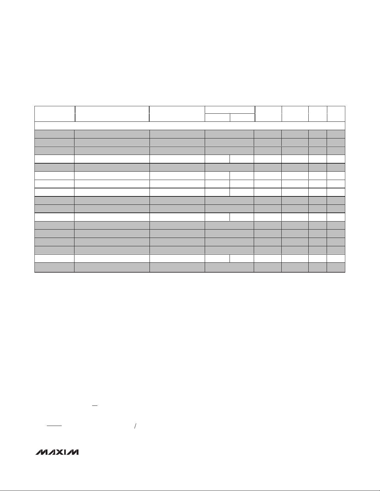
MAX16064
±0.3% Accurate, Quad, Power-Supply Controller with
Active-Voltage Output Control and PMBus Interface
______________________________________________________________________________________ 33
Table 4. MAX16064 PMBus Command Summary (continued)
(Global commands are shaded; they are not dependent on the PAGE)
PAGE
COMMAND
CODE
COMMAND NAME
TRANSACTION
TYPE
0-3 255
NO. OF
mbR
MANUFACTURER-SPECIFIC COMMANDS
D0h MFR_SMB_LOOPBACK R/W Word R/W 2 —
—
D1h MFR_MODE R/W Word R/W 2 —
—
D3h MFR_SAMPLE_RATE R/W Word R/W 2 —
—
D4h MFR_VOUT_PEAK Read Word R/W R/W 2
0-1
D6h MFR_TEMPERATURE_PEAK Read Word R/W 2 7612
-3
D8h MFR_STATUS_WORD R/W Word R R 2 —
—
D9h MFR_FAULT_RESPONSE R/W Word R/W W 2 —
—
DAh MFR_FAULT_RETRY R/W Word R/W W 2 —
—
DBh MFR_SET_ADDRESS R/W Byte R/W 1 —
—
DDh MFR_RESET_DELAY R/W Word R/W 2 1 0 1
DEh MFR_MODE_OUTPUT R/W Word R/W W 2 —
—
DFh MFR_VLTO R/W Byte R/W 1 —
—
E0h MFR_DAC_ACT_CNT R/W Byte R/W 1 —
—
E1h MFR_RESET_OUTPUT R/W Byte R/W 1 —
—
E2h MFR_FAULT_REASON R/W Word R/W 2 —
—
E3h MFR_FAULT_VOUT R/W Word R/W W 2 —
—
E4h MFR_FAULT_TEMP R/W Word R/W 2 —
—
The following example demonstrates how the host can
send and retrieve values from the MAX16064.
From Table 4, the coefficients used in the following
parameters are:
VOUT_COMMAND: m = 19995, b = 0, R = -1
READ_VOUT: m = 19995, b = 0, R = -1
If a host wants to command the power supply to output a
voltage of 3.0V, the corresponding VOUT_COMMAND
value is:
Y = (mX + b) x 10
R
Y = (19995 x 3.0 + 0) x 10-1= 5998.5
(decimal) = 176Eh (hex)
Conversely, if the host received a value of 176Eh on a
READ_VOUT command, this is equivalent to:
Power supplies and power converters generally have
no way of knowing how their outputs are connected to
ground. Within the power supply, all output voltages are
most commonly treated as positive. Accordingly, all
output voltages and output voltage-related parameters
of PMBus devices are commanded and reported as
positive values. It is up to the system to know that a
particular output is negative if that is of interest to the
system.
All output voltage-related commands use 2 data bytes.
Fault Management and Reporting
For reporting faults/warnings to the host on a real-time
basis, the MAX16064 asserts the open-drain
SMBALERT pin and sets the appropriate bit in the
STATUS_BYTE and MFR_FAULT_STATUS registers,
respectively. On recognition of the SMBALERT asser-
tion, the host or system manager is expected to poll the
I
2
C bus to determine the device asserting SMBALERT.
The host sends the SMBus Alert Response Address
(0001100). The MAX16064 will ACK the SMBus Alert
Response Address, transmit its slave address, and
deassert SMBALERT. The system controller then
BYTES
—
—
—
19995
335
—
—
—
—
—
—
—
—
—
—
—
XEh=×−
1
19995
1
X
Yb
=×−
()
m
−−
176 10 0 59980 19995 2 9
()
0 0083 3 0.%..which is within of V
1()
R
−
10
==
.999750
Page 34

MAX16064
±0.3% Accurate, Quad, Power-Supply Controller with
Active-Voltage Output Control and PMBus Interface
34 ______________________________________________________________________________________
communicates with PMBus commands to retrieve the
fault/warning status information from the MAX16064.
The following status commands are supported:
STATUS_BYTE
STATUS_WORD
STATUS_VOUT
STATUS_TEMPERATURE
STATUS_CML
STATUS_MFR_SPECIFIC
MFR_STATUS_WORD
MFR_FAULT_REASON
MFR_FAULT_VOUT
MFR_FAULT_TEMP
See the individual command sections for more details.
Faults/warnings are cleared when any one of the following conditions occurs:
• A CLEAR_FAULTS command is received.
• OPERATION commands are received that turn off and
on the power supplies or A3/CONTROL is toggled to
turn off and then turn on the power supplies.
• Bias power (AVDD, DVDD) to the MAX16064 is
removed and then reapplied.
The MAX16064 responds to fault conditions according
to the Manufacturer Fault Response command
(MFR_FAULT_RESPONSE). This command byte determines how the MAX16064 should respond to each particular fault. In addition, the MAX16064 responds to the
following error conditions.
1) If the internal reference fails to operate, SMBALERT
is asserted. To clear this fault, the MAX16064 must
go through a device reset.
2) The MAX16064 responds to unsupported com-
mands with a NACK.
3) When the host sends insufficient data (too few
bytes), the MAX16064 sets the CML bit and asserts
SMBALERT.
4) When the host sends too much data (too many
bytes), the MAX16064 sets the CML bit and asserts
SMBALERT.
When a read request is issued to a write-only command, the read operation is aborted and no warning is
issued.
PMBus Commands
A summary of the PMBus commands supported by the
MAX16064 is described in Table 4.
PAGE (00h)
The MAX16064 can control up to four power supplies
using one PMBus (I2C) address. Send the PAGE command with data 0 to 3 to select which power supply is
affected by all following commands. Set the PAGE to
255 when it is desired that following commands affect
all four power supplies. If, when PAGE = 255, the host
sends a command code that is not a global command
(any command in Table 4 that is not shaded), the
MAX16064 sets the CML, error flag. An example would
be to set the PAGE to 255 and then issue an OPERATION command to turn on all the power supplies at
one time.
OPERATION (01h)
The OPERATION command is used to turn the power
supply on and off in conjunction with ENOUT_ according
to the ENOUT_ polarity select setup. The OPERATION
command is also used to cause the power supply to set
the output voltage to the upper or lower margin voltages.
The power supply stays in the commanded operating
mode until a subsequent OPERATION command or
change in the state of A3/CONTROL (if enabled)
instructs the power supply to change to another state.
The valid OPERATION command byte values are
shown in Table 5.
The OPERATION command controls how the MAX16064
responds when commanded to change the output. When
the command byte is 00h, the MAX16064 immediately
turns the power supply off and ignores any programmed
turn-off delay and fall time. When the command byte is
set to 40h, the MAX16064 powers down according to the
programmed turn-off delay and fall time.
In Table 5, Act On Fault means that if an output overvoltage warning or output overvoltage fault is detected
when the output is margined high, the MAX16064 treats
this as a warning or fault and responds as programmed
by the warning limit or fault response command.
Similarly, if an output undervoltage warning or output
undervoltage fault is detected when the output is margined low, the MAX16064 treats this as a qualified
warning/fault event and responds as programmed by
the warning/fault limit or fault response command.
Any command value not shown in Table 5 is an invalid
command. If the MAX16064 receives a data byte that is
not listed in Table 5, then it may treat this as invalid
data, declares a communications fault (set CML bit and
assert SMBALERT), and responds as described in the
Fault Management and Reporting
section.
The default OPERATION value is 00h.
Page 35

MAX16064
±0.3% Accurate, Quad, Power-Supply Controller with
Active-Voltage Output Control and PMBus Interface
______________________________________________________________________________________ 35
ON_OFF_CONFIG (02h)
The ON_OFF_CONFIG command configures the combination of CONTROL input and serial bus commands
needed to turn the power supply on and off. This indicates how the power supply is commanded when
power is applied. The ON_OFF_CONFIG message content is described in Table 6.
CLEAR_FAULTS (03h)
The CLEAR_FAULTS command is used to clear any
fault bits that have been set. This command clears all
bits in the STATUS_BYTE and MFR_FAULT_STATUS
registers simultaneously. It also deasserts SMBALERT.
The CLEAR_FAULTS command does not cause a
power supply that has latched off for a fault condition to
Table 5. OPERATION Command Byte
COMMAND BYTE POWER SUPPLY ON OR OFF MARGIN STATE
00h Immediate off (no sequencing) —
40h Soft-off (with sequencing) —
80h On Margin off (nominal)
94h On Margin low (ignore fault)
98h On Margin low (act on fault)
A4h On Margin high (ignore fault)
A8h On Margin high (act on fault)
Table 6. ON_OFF_CONFIG Message Contents
BIT NUMBER
PURPOSE MEANING
[7:5] Reserved. Always returns 000.
4
Sets the default to operate either any
time power is present or for the on/off to
be controlled by A3/CONTROL input
and serial bus commands
0 = Power supply turns on (ENOUT goes high) any time power is
present regardless of the state of the A3/CONTROL pin.
1 = Power supply is not turned on until commanded by the
CONTROL pin and OPERATION command (as configured in bits
[3:0]).
3
Controls how the power supply
responds to commands received over
the serial bus
0 = Power supply ignores the on/off portion of the OPERATION
command received from the serial bus.
1 = An operation command must be received to turn the power supply
on. Depending on bit [2], the MAX16064 may require the
A3/CONTROL input to be asserted for the power supply to be
turned on (ENOUT asserted).
2
Configures how the power supply
responds to the A3/CONTROL input
0 = Power supply ignores the A3/CONTROL input. On/off is only
controlled by the OPERATION command.
1 = Power supply requires the A3/CONTROL input to be asserted to
turn on the power supply. Depending on bit [3], the MAX16064 may
require the OPERATION command to be received for the power
supply to be turned on (ENOUT asserted).
1 Polarity of the A3/CONTROL input
0 = A3/CONTROL input is active low. Drive low to turn on the power
supply.
1 = A3/CONTROL input is active high. Drive high to turn on the power
supply.
0
A3/CONTROL input action when
commanding the power supply to
turn off
0 = Use the configured turn off delay (TOFF_DELAY) and fall time
(TOFF_FALL).
1 = Turn off the power supply as quickly as possible (deassert ENOUT).
Page 36

MAX16064
±0.3% Accurate, Quad, Power-Supply Controller with
Active-Voltage Output Control and PMBus Interface
36 ______________________________________________________________________________________
restart. The status of ENOUT_ under fault conditions is
not affected by this command and should change only
if commanded through the OPERATION command or
A3/CONTROL.
If the fault is still present after the CLEAR_FAULTS command is executed, the fault bit is set again and the host
is also notified by asserting SMBALERT.
This command is write-only. There is no data byte for
this command.
WRITE_PROTECT (10h)
The WRITE_PROTECT command is used to provide
protection against accidental changes to the
MAX16064 operating memory. All supported commands may have their parameters read, regardless of
the WRITE_PROTECT settings. The WRITE_PROTECT
message content is described in Table 7.
STORE_DEFAULT_ALL (11h)
The STORE_DEFAULT_ALL command instructs the
MAX16064 to transfer the user memory configuration
information to an external I2C EEPROM device (default
memory) attached to A1/SCLE and A2/SDAE. If an error
occurs during the transfer, SMBALERT asserts and the
CML bit is set to 1.
It is permitted to use the STORE_DEFAULT_ALL command while the power supply is operating. However,
the MAX16064 is unresponsive to PMBus commands
while transferring the configuration. ENOUT_ maintains
its state.
This command is write-only. There is no data byte for
this command.
For information on EEPROM contents, see the
External
EEPROM Interface
section.
RESTORE_DEFAULT_ALL (12h)
The RESTORE_DEFAULT_ALL command transfers the
default configuration information from the external I2C
EEPROM device attached to A1/SCLE and A2/SDAE to
the user memory registers in the device. The
RESTORE_DEFAULT_ALL command can only be executed when the power supply is off. Otherwise, a communication fault occurs (CML = 1) and SMBALERT
asserts. If an error occurs during data transfer,
SMBALERT asserts and the CML bit is set to 1.
The STATUS_BYTE, STATUS_WORD and
MFR_FAULT_STATUS values are not restored by the
RESTORE_DEFAULT_ALL command.
This command is write-only. There is no data byte for
this command.
For information on EEPROM contents, see the
External
EEPROM Interface
section.
CAPABILITY (19h)
The CAPABILITY command is used to determine some
key capabilities of the MAX16064. The CAPABILITY
command is read-only. The message content is
described in Table 8.
Table 7. WRITE_PROTECT Message Contents
DATA BYTE VALUE MEANING
1000 0000 Disable all writes except the WRITE_PROTECT command.
0100 0000 Disable all writes except the WRITE_PROTECT, OPERATION, and PAGE commands.
0010 0000
Disable all writes except the WRITE_PROTECT, OPERATION, PAGE, ON_OFF_CONFIG, and
VOUT_COMMAND commands.
0000 0000 Enable writes for all commands (default)
Table 8. CAPABILITY Command Message Contents
BIT DESRIPTION MEANING
7 Packet error checking 1 = Packet error checking is supported. Always returns a 1.
6:5 Maximum PMBus bus speed 00 = Maximum supported bus speed is 100kHz.
4 SMBALERT#
1 = Device supports an SMBALERT# output and the SMBus ARA
protocol.
3:0 Reserved MAX16064 returns 0000.
Page 37

MAX16064
±0.3% Accurate, Quad, Power-Supply Controller with
Active-Voltage Output Control and PMBus Interface
______________________________________________________________________________________ 37
VOUT_MODE (20h)
The VOUT_MODE command is used to report the data
format of the device. The MAX16064 uses the direct format for all the voltage-related commands. The value
returned is 40h, indicating DIRECT data format. This
command is read only. See Table 4 for the m, b, and R
values for the various commands.
VOUT_COMMAND (21h)
The VOUT_COMMAND command loads the MAX16064
with the voltage to which the power-supply output is to
be changed when it is commanded to turn on using the
OPERATION command or A3/CONTROL transition
when enabled. Once the power supply is turned on,
changing the VOUT_COMMAND has no effect on the
power-supply output voltage. The MAX16064 only
adjusts the power supply to the new VOUT_COMMAND
voltage after receiving a new turn-on command.
The two data bytes are in DIRECT format. Valid values
are from 0 to 2.0V when the input range is 2.0V, and 0 to
5.5V when the input range is 5.5V. See the
MFR_MODE_OUTPUT (DEh)
section for more information.
The default VOUT_COMMAND value is 00h.
VOUT_MARGIN_HIGH (25h)
The VOUT_MARGIN_HIGH command loads the
MAX16064 with the voltage to which the power-supply
output is to be changed when the OPERATION command is set to margin high. If the power supply is
already operating at margin high, changing
VOUT_MARGIN_HIGH has no effect on the output voltage. The MAX16064 only adjusts the power supply to
the new VOUT_MARGIN_HIGH voltage after receiving a
new margin high OPERATION command.
The two data bytes are in DIRECT format. Valid values
are the same as VOUT_COMMAND.
The default VOUT_MARGIN_HIGH value is 00h.
VOUT_MARGIN_LOW (26h)
The VOUT_MARGIN_LOW command loads the
MAX16064 with the voltage to which the power-supply
output is to be changed when the OPERATION command is set to margin low. If the power supply is
already operating at margin low, changing
VOUT_MARGIN_LOW has no effect on the output voltage. The MAX16064 only adjusts the power supply to
the new VOUT_MARGIN_LOW voltage after receiving a
new margin low OPERATION command.
The two data bytes are in DIRECT format. Valid values
are the same as VOUT_COMMAND.
The default VOUT_MARGIN_LOW value is 00h.
VOUT_TRANSITION_RATE (27h)
The VOUT_TRANSITION_RATE command sets the rate
in mV/µs at which the power-supply output voltage
should change when the power supply is commanded
to change among the margin high, margin low, and
margin off (ON) OPERATION mode. This commanded
rate of change does not apply when the power supply
is commanded to turn on or off. In that case, t
ON_RISE
and t
OFF_FALL
apply.
The two data bytes are in DIRECT format. Valid values
are from 0 to 128mV/µs (FB mode) or 0.004 to 30mV/µs
(REFIN mode).
The default VOUT_TRANSITION_RATE value is 0.
When VOUT_TRANSITION_RATE is cleared to 0,
VOUT_TRANSITION_RATE is ignored and the voltage output is not changed even when commanded by the
OPERATION command. When VOUT_TRANSITION_RATE
is set to 07FFFh, the voltage output is adjusted as quickly
as possible. If a VOUT_TRANSITION_RATE parameter
results in the DAC outputting an out of range value (valid
range 0 to 4090) during transition, the CML flag is set and
SMBALERT is asserted to issue a warning.
The VOUT_TRANSITION_RATE command applies to
REFIN mode only and is ignored in feedback mode.
VOUT_SCALE_LOOP (29h)
In applications where the V
OUT
is not equal to the voltage at REFIN, VOUT_SCALE_LOOP is used. For example, if REFIN expects a 0.6V input for a 3.3V output,
VOUT_SCALE_LOOP = 0.6V/3.3V = 0.182.
In applications where the power-supply output voltage is
greater than the MAX16064 input range, the output voltage
of the power supply is sensed through a resistive voltagedivider, as illustrated in Figure 16. The resistive voltagedivider reduces or scales the output voltage, V
OUT
.
The PMBus commands specify the actual power-supply
output voltages and not the input voltage to the control
circuit. To allow the MAX16064 to map between the
commanded voltage (such as 3.3V), and the voltage at
the control circuit input (perhaps 3.3V divided down to
match a reference voltage of 2.0V), the
VOUT_SCALE_LOOP command is used.
The two data bytes are in DIRECT format. Valid values
are from 0 to 1.0. Note that due to m, b, r representation
restriction, the supplied value is rounded off to multiples of 1/128. Therefore, to ensure optimum operation,
circuit design should choose a value as close as possible to multiples of 1/128 to avoid rounding errors affect-
VOUT SCALE L OOP
__=
R
RR
+212
Page 38

ing the VOUT_TRANSITION_RATE slew rate. Final
accuracy of V
OUT
is assured by the closed-loop volt-
age control.
This value is dimensionless.
The default VOUT_SCALE_LOOP value is 00h.
The VOUT_SCALE_LOOP command is ignored in feedback mode.
VOUT_OV_FAULT_LIMIT (40h)
The VOUT_OV_FAULT_LIMIT command sets the value
of the output voltage measured across RS_+ and RS_-,
which causes an output overvoltage fault.
The two data bytes are in DIRECT format. Valid values
are the same as VOUT_COMMAND.
The default VOUT_OV_FAULT_LIMIT value is 00h.
In response to the VOUT_OV_FAULT_LIMIT being
exceeded, the MAX16064:
1) Sets the VOUT_OV bit in the STATUS_BYTE.
2) Sets the VOUT_OV bit in the STATUS_WORD.
3) Sets bit 5 (low byte) and bit 7 (high byte) of the
STATUS_WORD.
4) Sets the VOUT Overvoltage Fault bit in the STATUS_VOUT.
5) Sets the VOUT_OV bit in the MFR_STATUS_WORD
register.
6) Responds as specified by VOUT_OV_FAULT_
RESPONSE bits in the MFR_FAULT_RESPONSE
register.
7) Notifies the host through SMBALERT assertion.
VOUT_OV_WARN_LIMIT (42h)
The VOUT_OV_WARN_LIMIT command sets the value
of the output voltage measured across RS_+ and RS_-,
which causes an output voltage high warning. This
value is typically less than the output overvoltage
threshold in VOUT_OV_FAULT_LIMIT.
The two data bytes are in DIRECT format. Valid values
are the same as the VOUT_COMMAND.
The default VOUT_OV_WARN_LIMIT value is 00h.
In response to the VOUT_OV_WARN_LIMIT being
exceeded, the MAX16064:
1) Sets the OTHER bit in the STATUS_BYTE.
2) Sets the OTHER bit in the STATUS_WORD.
3) Sets the VOUT bit in the STATUS_WORD.
4) Sets the VOUT Overvoltage Warning bit in the
STATUS_VOUT.
5) Sets the OV_WARN bit in the STATUS_MFR_SPECIFIC
register.
6) Sets the OV_WARN bit in the MFR_STATUS_WORD
register.
7) Sets the OTHER bit in the MFR_STATUS_WORD.
8) Notifies the host using SMBALERT assertion.
VOUT_UV_WARN_LIMIT (43h)
The VOUT_UV_WARN_LIMIT command sets the value
of the output voltage measured across RS_+ and RS_-,
which causes an output-voltage low warning. This value
is typically greater than the output undervoltage fault
threshold in VOUT_UV_FAULT_LIMIT.
This warning is masked until the output voltage reaches
the programmed voltage at startup, and also during
turn-off when the power supply is disabled.
The two data bytes are in DIRECT format. Valid values
are the same as VOUT_COMMAND.
The default VOUT_UV_WARN_LIMIT value is 00h.
In response to violation of the VOUT_UV_WARN_LIMIT,
the MAX16064:
1) Sets the OTHER bit in the STATUS_BYTE.
2) Sets the OTHER bit in the STATUS_WORD.
3) Sets the VOUT bit in the STATUS_WORD.
4) Sets the VOUT Undervoltage Warning bit in the
STATUS_VOUT register.
5) Sets the UV_WARN bit in the STATUS_MFR_SPECIFIC register.
6) Sets the UV_WARN bit in the MFR_STATUS_WORD
register.
7) Sets the OTHER bit in the MFR_STATUS_WORD.
8) Notifies the host using SMBALERT assertion.
MAX16064
±0.3% Accurate, Quad, Power-Supply Controller with
Active-Voltage Output Control and PMBus Interface
38 ______________________________________________________________________________________
Figure 18. VOUT_SCALE_LOOP
RS_-
MAX16064
R
RS_+
1
R
2
VO+
LOAD
POWER
SUPPLY
VO-
Page 39

MAX16064
±0.3% Accurate, Quad, Power-Supply Controller with
Active-Voltage Output Control and PMBus Interface
______________________________________________________________________________________ 39
VOUT_UV_FAULT_LIMIT (44h)
The VOUT_UV_FAULT_LIMIT command sets the value
of the output voltage measured across RS_+ and RS_-,
which causes an output undervoltage fault. This fault is
masked until the output voltage reaches the programmed voltage at startup, and also during turn-off
when the power supply is disabled.
The 2 data bytes are in DIRECT format. Valid values are
the same as VOUT_COMMAND.
The default VOUT_UV_FAULT_LIMIT value is 00h.
In response to violation of the VOUT_UV_FAULT_LIMIT,
the MAX16064:
1) Sets the OTHER bit in the STATUS_BYTE.
2) Sets the OTHER bit in the STATUS_WORD.
3) Sets the VOUT bit in the STATUS_WORD.
4) Sets the VOUT Undervoltage Fault bit in the
STATUS_VOUT register.
5) Sets the UV_FAULT bit in the STATUS_MFR_SPECIFIC
register.
6) Sets the UV_FAULT bit in the MFR_STATUS_WORD
register.
7) Sets the OTHER bit in the MFR_STATUS_WORD.
8) Responds as specified by VOUT_UV_FAULT_RESPONSE
bits in the MFR_FAULT_RESPONSE register.
9) Notifies the host using SMBALERT assertion.
OT_FAULT_LIMIT (4Fh)
The OT_FAULT_LIMIT command sets the temperature,
in degrees Celsius, of the on-chip temperature sensor
at which an overtemperature fault is detected.
The 2 data bytes are in DIRECT format. Valid values are
from -142.5°C to +395.4°C.
The default OT_FAULT_LIMIT value is 00h.
In response to the OT_FAULT_LIMIT being exceeded,
the MAX16064:
1) Sets the TEMPERATURE bit in the STATUS_BYTE.
2) Sets the TEMPERATURE bit in the STATUS_WORD.
3) Sets the TEMPERATURE bit in the
MFR_STATUS_WORD.
4) Sets the Overtemperature Fault bit in the
STATUS_TEMPERATURE.
5) Sets the OT_FAULT bit in the MFR_STATUS_WORD
register.
6) Responds as specified by OT_FAULT_RESPONSE
bits in the MFR_FAULT_RESPONSE register.
7) Notifies the host using SMBALERT assertion.
OT_WARN_LIMIT (51h)
The OT_WARN_LIMIT command sets the temperature,
in degrees Celsius, of the on-chip temperature sensor
at which an overtemperature warning is detected.
The 2 data bytes are in DIRECT format. Valid values are
the same as the OT_FAULT_LIMIT.
The default OT_WARN_LIMIT value is 00h.
In response to the OT_WARN_LIMIT being exceeded,
the MAX16064:
1) Sets the TEMPERATURE bit in the STATUS_BYTE.
2) Sets the TEMPERATURE bit in the STATUS_WORD.
3) Sets the TEMPERATURE bit in the
MFR_STATUS_WORD.
4) Sets the Overtemperature Warning bit in the
STATUS_TEMPERATURE.
5) Sets the OT_WARN bit in the MFR_STATUS_WORD
register.
6) Notifies the host through SMBALERT using asser-
tion.
TON_DELAY (60h)
TON_DELAY sets the time, in milliseconds, from when a
start condition is received (a valid OPERATION command or through A3/CONTROL when enabled) until the
power-supply output voltage starts to rise. During
TON_DELAY, the power supply is disabled (ENOUT_
deasserted) until TON_DELAY expires. Also, the undervoltage fault and warning are masked off during
TON_DELAY.
The 2 data bytes are in DIRECT format. Valid values are
from 0 to 3276.7ms.
The default TON_DELAY value is 0.
TON_RISE (61h)
The TON_RISE sets the time, in milliseconds, from
when the power-supply output voltage starts to rise until
the voltage has entered the regulation band. During
TON_RISE, the voltage and temperature-related faults
and warnings are masked off. Meanwhile, the
MAX16064 still responds to the PMBus command. If a
TON_RISE parameter results in the DAC outputting an
out-of-range value (valid range 0 to 4090) immediately
during TON_RISE, the CML flag is set and SMBALERT
asserts to issue a warning.
Page 40

MAX16064
±0.3% Accurate, Quad, Power-Supply Controller with
Active-Voltage Output Control and PMBus Interface
40 ______________________________________________________________________________________
Table 9. STATUS_BYTE Message Contents
BIT NUMBER
STATUS BIT NAME
MEANING
7 BUSY
A fault was declared because the device was busy and unable to respond.
(The BUSY bit is not supported. This bit always returns 0).
6 OFF
This bit is asserted if ENOUT is presently disabling the power supply, regardless of the
reason, including simply not being enabled.
5 VOUT_OV An output overvoltage fault has occurred.
4 IOUT_OC
An output overcurrent fault has occurred.
(The IOUT_OC bit is not supported. This bit always returns 0).
3 VIN_UV
An input undervoltage fault has occurred.
(The VIN_UV bit is not supported. This bit always returns 0).
2 TEMPERATURE A temperature fault or warning has occurred.
1 CML A communication, memory, or logic fault has occurred.
0 OTHER
A fault or warning not listed in bits [7:1] has occurred. See the MFR_STATUS_WORD (D8h)
section for more information.
In feedback mode, the MAX16064 leaves the S_ switch
on the DAC open during soft-start. It waits for the
TON_RISE time to expire before adjusting the DAC output to equal the DACOUT_ feedback and then closes
the S_ switch.
The 2 data bytes are in DIRECT format. In REFIN mode,
the TON_RISE parameter is a 16-bit value and the valid
values are from 0.01ms to 32.767ms. In FB mode, the
TON_RISE is a 14-bit value and the valid values are
from 0.01ms to 16.383ms (the upper 2 bits are ignored).
The default TON_RISE value is 0.01ms. Setting any
value less than this minimum value defaults to 0.01ms.
TOFF_DELAY (64h)
The TOFF_DELAY sets the time, in milliseconds, from
when a STOP condition is received (a soft-off OPERATION command or through A3/CONTROL when
enabled) until the power supply stops transferring energy to the output.
When commanded to turn off immediately through the
OPERATION command, the TOFF_DELAY value is
ignored. When commanded to turn off through
A3/CONTROL (when enabled) or EN, the TOFF_DELAY
parameter is used.
The 2 data bytes are in DIRECT format. Valid values are
from 0 to 3276.7ms.
The default TOFF_DELAY value is 0.
TOFF_FALL (65h)
The TOFF_FALL command sets the time, in milliseconds, from the end of the turn-off delay time until the
output voltage is commanded to zero. Note that this
command can only be used with a device whose output
can sink enough current to cause the output voltage to
decrease at a controlled rate.
When commanded to turn off immediately through the
OPERATION command, the TOFF_FALL value is
ignored. When commanded to turn off through the
OPERATION soft-off command or A3/CONTROL (when
enabled) or EN, the TOFF_FALL parameter is used. If a
TOFF_FALL parameter results in the DAC outputting an
out-of-range value (valid range 0 to 4090) immediately
during TOFF_FALL, the CML flag is set and SMBALERT
asserts to issue a warning.
In feedback mode, this value is not used. The
MAX16064 disables ENOUT_ and opens the DAC
switch immediately after the TOFF_DELAY.
The 2 data bytes are in DIRECT format. Valid values are
from 0.01ms to 32.767ms.
Do not set TOFF_FALL to any value less than 0.1ms.
STATUS_BYTE (78h)
The STATUS_BYTE command returns 1 byte of information with a summary of the most critical faults. A value
of 1 indicates that a fault or warning event has occurred
and a 0 indicates otherwise. Bits for unsupported features shall be reported as 0.
The STATUS_BYTE cannot be restored by
RESTORE_DEFAULT_ALL command. The STATUS_BYTE
message content is described in Table 9.
This command is read only.
The default STATUS_BYTE value is 40h (power supply
is off).
Page 41

MAX16064
±0.3% Accurate, Quad, Power-Supply Controller with
Active-Voltage Output Control and PMBus Interface
______________________________________________________________________________________ 41
Table 10. STATUS_WORD Message Contents
BYTE
BIT
STATUS BIT NAME MEANING
7 VOUT An output-voltage fault or warning has occurred.
6 IOUT/POUT The IOUT/POUT bit is not supported. This bit always returns 0.
5 INPUT The INPUT bit is not supported. This bit always returns 0.
4 MFR A manufacturer-specific fault or warning has occurred.
3 POWER_GOOD# The POWER_GOOD# bit is not supported. This bit always returns 0.
2 FANS The FANS bit is not supported. This bit always returns 0.
1 OTHER Reserved.
High
0 UNKNOWN A fault type not given in bits [15:1] of the STATUS_WORD has been detected.
7 BUSY
A fault was declared because the device was busy and unable to respond. The
BUSY bit is not supported. This bit always returns 0.
6 OFF
This bit is asserted if ENOUT is presently disabling the power supply,
regardless of the reason, including simply not being enabled.
5 VOUT_OV An output overvoltage fault has occurred.
4 IOUT_OC
An output overcurrent fault has occurred. The IOUT_OC bit is not supported.
This bit always returns 0.
3 VIN_UV
An input undervoltage fault has occurred. The VIN_UV bit is not supported. This
bit always returns 0.
2 TEMPERATURE A temperature fault or warning has occurred.
1 CML A communication, memory, or logic fault has occurred.
Low
0 OTHER
A fault or warning not listed in bits [7:1] has occurred. See the
MFR_STATUS_WORD (D8h) section for more information.
Table 11. STATUS_VOUT Message Contents
BIT NUMBER MEANING
7 VOUT overvoltage fault
6 VOUT overvoltage warning
5 VOUT undervoltage fault
4 VOUT undervoltage warning
3
VOUT_MAX warning
This bit is not supported. This bit always returns 0.
2
TON_MAX_FAULT
This bit is not supported. This bit always returns 0.
1
TOFF_MAX_WARNING
This bit is not supported. This bit always returns 0.
0
VOUT tracking error
This bit is not supported. This bit always returns 0.
STATUS_WORD (79h)
The STATUS_WORD command returns two bytes of
information with a summary of the reason for a fault.
The low byte of the STATUS_WORD is the same data
as the STATUS_BYTE. The STATUS_WORD message
content is described in Table 10.
STATUS_VOUT (7Ah)
The STATUS_VOUT command returns one byte of information with contents as described in Table 11.
NUMBER
Page 42

MAX16064
±0.3% Accurate, Quad, Power-Supply Controller with
Active-Voltage Output Control and PMBus Interface
42 ______________________________________________________________________________________
Table 12. STATUS_TEMPERATURE Message Contents
BIT NUMBER MEANING
7 Overtemperature fault
6 Overtemperature warning
5
Undertemperature fault
This bit is not supported. This bit always returns 0.
4
Undertemperature warning
This bit is not supported. This bit always returns 0.
3 Reserved
2 Reserved
1 Reserved
0 Reserved
Table 13. STATUS_CML Message Contents
BIT NUMBER MEANING
7 Invalid or unsupported command received
6 Invalid or unsupported data received
5 Packet error check (PEC) failed
4
Memory fault detected
This bit is not supported. This bit always returns 0.
3
Processor fault detected
This bit is not supported. This bit always returns 0.
2 Reserved
1
A communication fault other than the ones listed in this table has occurred.
This bit is not supported. This bit always returns 0.
0
Other memory of logic fault has occurred.
This bit is not supported. This bit always returns 0.
Table 14. STATUS_MFR_SPECIFIC Message Contents
BIT NUMBER
STATUS BIT NAME
MEANING
7 EN_FAULT EN input is below its threshold when OPERATION is on.
6 OT_WARN Overtemperature warning (same as STATUS_TEMPERATURE bit 6).
5 OT_FAULT Overtemperature fault (same as STATUS_TEMPERATURE bit 7).
4 ADCERR_FAULT An ADC conversion fault has occurred.
3 N/A This bit is reserved and always returns 0.
2 UV_WARN A VOUT undervoltage warning has occurred (same as STATUS_VOUT bit 4).
1 UV_FAULT A VOUT undervoltage fault has occurred (same as STATUS_VOUT bit 5).
0 OV_WARN A VOUT overvoltage warning has occurred (same as STATUS_VOUT bit 6).
STATUS_TEMPERATURE (7Dh)
The STATUS_TEMPERATURE command returns one byte
of information with contents as described in Table 12.
STATUS_CML (7Eh)
The STATUS_CML command returns one byte of information with contents as described in Table 13.
STATUS_MFR_SPECIFIC (80h)
The STATUS_MFR_SPECIFIC command returns one
byte of information with a summary of the reason for a
fault. The STATUS_MFR_SPECIFIC message content is
described in Table 14.
Page 43

READ_VOUT (8Bh)
The READ_VOUT command returns the actual measured (not commanded) output voltage across RS_+
and RS_-. If filter mode is enabled, the filtered value is
returned.
The 2 data bytes are in DIRECT format. Valid values are
the same as VOUT_COMMAND.
The default READ_VOUT value is 00h.
READ_TEMPERATURE_1 (8Dh)
The MAX16064 supports only one temperature reading,
READ_TEMPERATURE_1. The MAX16064 returns the
actual on-chip measured temperature in degrees
Celsius.
The 2 data bytes are in DIRECT format. Valid values are
the same as OT_FAULT_LIMIT.
The default READ_TEMPERATURE_1 value is 00h.
PMBUS_REVISION (98h)
The PMBUS_REVISION command returns the revision
of the PMBus specification to which the MAX16064 is
compliant.
The command has 1 data byte. Bits [7:5] indicate the
revision of PMBus specification Part I to which the
MAX16064 is compliant. Bits [4:0] indicate the revision
of PMBus specification Part II to which the MAX16064 is
compliant. The values are shown in Table 15.
This command is read only.
The PMBUS_REVISION value returned is 00h which
indicates that the MAX16064 is compliant with Part I
Rev 1.0 and Part II Rev 1.0.
MFR_ID (99h)
The MFR_ID command returns the MAX16064 manufacturer’s identification.
The default MFR_ID value is 4Dh (M).
This command is read only.
MFR_MODEL (9Ah)
The MFR_MODEL command returns the MAX16064
model number.
The default MFR_MODEL value is 43h (C).
This command is read only.
MFR_REVISION (9Bh)
The MFR_REVISION command reads the ASCII characters that contain the MAX16064 revision number with a
block read command.
The default MFR_REVISION value is 31h (1).
This command is read only.
MFR_LOCATION (9Ch)
The MFR_LOCATION command loads the device with
text (ISO/IEC 8859-1) characters that identify the facility
that manufactures the power supply. The maximum
number of characters is 20. This can be written to external EEPROM using the STORE_DEFAULT_ALL command. If an external EEPROM is not used, the
command returns the text string MXIM.
MFR_DATE (9Dh)
The MFR_DATE command loads the device with text
(ISO/IEC 8859-1) characters that identify the date of
manufacture of the power supply. The maximum number of characters is 8. This can be written to external
EEPROM using the STORE_DEFAULT_ALL command.
If an external EEPROM is not used, the command
returns the text string 080416.
MFR_SERIAL (9Eh)
The MFR_SERIAL command loads the device with text
(ISO/IEC 8859-1) characters that uniquely identify the
power supply. The maximum number of characters is
16. This can be written to external EEPROM using the
STORE_DEFAULT_ALL command. If an external
EEPROM is not used, the command returns the text
string 00000000.
USER_DATA_00 (B0h)
The USER_DATA_00 command loads the device with
user data. The maximum number of bytes is 40. This can
be written to external EEPROM using the
STORE_DEFAULT_ALL command. If an external
EEPROM is not used, the command returns 00h for all
bytes.
MFR_SMB_LOOPBACK (D0h)
The MFR_SMB_LOOPBACK command returns the data
word previously received by the MAX16064. The
SMBus master writes a data word to the MAX16064
using this command and then retrieves the data word.
A valid communication channel is established if the
master reads back the same word.
Note that if another command is sent in between the
write MFR_SMB_LOOPBACK command and the read
MFR_SMB_LOOPBACK command, the MAX16064
returns whatever last command data word it receives.
MAX16064
±0.3% Accurate, Quad, Power-Supply Controller with
Active-Voltage Output Control and PMBus Interface
______________________________________________________________________________________ 43
Table 15. PMBus Revision Data Byte
Contents
BITS [7:5]
PART I
PART II
REVISION
000 1.0 00000 1.0
REVISION
BITS [4:0]
Page 44

MAX16064
±0.3% Accurate, Quad, Power-Supply Controller with
Active-Voltage Output Control and PMBus Interface
44 ______________________________________________________________________________________
Table 16. MFR_MODE Bit Definition
BIT BIT NAME DESCRIPTION
15:8
Input Clock Time
Factor
This is equivalent to the number of external clock cycles provided to CLKIO in 100_S - 2.
MFR_MODE[15:8] = f
EXT_CLK
/10kHz - 2 where f
EXT_CLK
is the frequency of the external clock. For
example, when f
EXT_CLK
= 1MHz, f
EXT_CLK
/10kHz = 100, MFR_MODE[15:8] = 100 – 2 = 98. Valid
external input clock range is from 100kHz (MFR_MODE[15:8] = 8) to 2.5MHz (MFR_MODE[15:8] =
248).
These bits are ignored if internal clock source is selected as the time base (Clock Source Select bit =
0).
7
Clock Out
Enable
The Clock Out Enable bit allows the output of a 1MHz reference clock to CLKIO for synchronizing
multiple MAX16064s.
1 = Enables the 1MHz output on CLKIO.
0 = Reference clock is not output (default).
6 IGNORE_EN
1 = The EN state is ignored and the MAX16064 is controlled according to ON_OFF_CONFIG.
0 = The MAX16064 turns on the external power supplies when EN exceeds its threshold. If EN goes
low after power-up, the MAX16064 turns off a power supply only if MFR_FAULT_RESPONSE[5:4] is
configured to do so.
5
EEPROM Lock
Enable
The EEPROM Lock Enable bit is used to protect external EEPROM data from being overwritten.
1 = The STORE_DEFAULT_ALL command is ignored. The RESTORE_DEFAULT_ALL command is still
valid.
0 = The STORE_DEFAULT_ALL command initiates a store configuration operation to the external
EEPROM attached to A1/SCLE and A2/SDAE (default).
4
Correction
Correction Bypass Enable.
1 = Disables a correction algorithm made to voltage and temperature readings.
0 = Applies a correction algorithm to temperature measurement, thus resulting in high-accuracy
readings. For optimal operation, this bit should be cleared to 0 (default).
3
EEPROM Fault
Lock
1 = EEPROM fault locations are locked. If a fault occurs, data is not written to the external EEPROM.
0 = EEPROM fault locations are unlocked. If a fault occurs, data is written to the external EEPROM.
2 PEC Enable
1 = PEC enabled for all commands.
0 = PEC is disabled (default).
1 Filter Setting
1 = Disable filtering of the voltage and temperature conversions.
0 = Enable filtering of the voltage and temperature conversions (default).
0
Clock Source
Select
The Clock Source Select bit determines the MAX16064 reference clock time source.
1 = An external clock must be supplied to CLKIO and is used as the MAX16064 reference clock.
0 = The internal clock is used.
MFR_MODE (D1h)
The MFR_MODE command is used to configure
the MAX16064 to support manufacturer specific
commands. The MFR_MODE command is described
in Table 16.
The default MFR_MODE value is 00h.
Bypass Enable
Page 45

MAX16064
±0.3% Accurate, Quad, Power-Supply Controller with
Active-Voltage Output Control and PMBus Interface
______________________________________________________________________________________ 45
Table 17. MFR_STATUS_WORD Bit Definition
MEANING
15 EN_FAULT EN input is below its threshold when OPERATION is on.
14 OT_WARN Overtemperature warning (Same as STATUS_TEMPERATURE bit 6).
13 OT_FAULT Overtemperature fault (Same as STATUS_TEMPERATURE bit 7).
12 ADCERR_FAULT An ADC conversion fault has occurred.
11 N/A This bit is reserved and always returns 0.
10 UV_WARN A VOUT undervoltage warning has occurred (same as STATUS_VOUT bit 4).
9 UV_FAULT A VOUT undervoltage fault has occurred (same as STATUS_VOUT bit 5).
8 OV_WARN A VOUT overvoltage warning has occurred (same as STATUS_VOUT bit 6).
7 BUSY
A fault was declared because the device was busy and unable to respond.
The BUSY bit is not supported. This bit always returns 0.
6 OFF
This bit is asserted if ENOUT is presently disabling the power supply, regardless of the
reason, including simply not being enabled.
5 VOUT_OV An output overvoltage fault has occurred.
4 IOUT_OC
An output overcurrent fault has occurred.
The IOUT_OC bit is not supported. This bit always returns 0.
3 VIN_UV
An input undervoltage fault has occurred.
The VIN_UV bit is not supported. This bit always returns 0.
2 TEMPERATURE A temperature fault or warning has occurred.
1 CML A communication, memory, or logic fault has occurred.
0 OTHER A fault or warning not listed in bits [7:1] has occurred.
MFR_SAMPLE_RATE (D3h)
The MFR_SAMPLE_RATE command sets the frequency
(Hz) at which the ADC conversion result registers (representing four voltages and one temperature) are compared with their threshold limits. This parameter does
not control the total ADC sampling rate, which is controlled by MFR_VLTO. Also, the output-voltage adjustment rate is not affected by this parameter.
Monitor Sample Frequency =
10kHz/MFR_SAMPLE_RATE
The 2 data bytes are formatted as positive integers. Valid
values are from 1 to 65535. Do not set this value to 0.
The default MFR_SAMPLE_RATE value is 50 which is
equivalent to a sample frequency of 200Hz.
MFR_VOUT_PEAK (D4h)
The MFR_VOUT_PEAK command returns the maximum
actual measured (not commanded) output voltage in
volts across RS_+ and RS_-. If the filter mode is
enabled, instead of returning the instantaneous value,
the filtered output voltage is returned. To reset this
value to 0, write to this command with a data value of 0.
Any other values written by this command are used as
a comparison for future peak updates.
The 2 data bytes are in DIRECT format. Valid values are
the same as VOUT_COMMAND.
The default MFR_VOUT_PEAK value is 0.
MFR_TEMPERATURE_PEAK (D6h)
The MFR_TEMPERATURE_PEAK command returns the
maximum actual on-chip measured temperature in
degrees Celsius. To reset this value to its lowest value,
write to this command with a data value of 0FFFFh. Any
other values written by this command are used as a
comparison for future peak updates.
The 2 data bytes are in DIRECT format. Valid values are
the same as OT_FAULT_LIMIT.
The default MFR_TEMPERATURE_PEAK value is 00h.
MFR_STATUS_WORD (D8h)
When a warning or fault condition is detected, the
MAX16064 sets the corresponding bit in the
MFR_STATUS_WORD register to 1 and notifies the host
using SMBALERT assertion. The MFR_STATUS_WORD
[7:0] (low byte) bits are the same definition and state as
the STATUS_BYTE command.
This register is cleared to 0 together with the STATUS_BYTE
register by any of the fault/warning clearing methods mentioned earlier in the CLEAR_FAULTS command.
The MFR_STATUS_WORD command value cannot be
restored by the RESTORE_DEFAULT_ALL command.
This command is read only.
BIT NUMBER STATUS BIT NAME
Page 46

MAX16064
±0.3% Accurate, Quad, Power-Supply Controller with
Active-Voltage Output Control and PMBus Interface
46 ______________________________________________________________________________________
Table 18. MFR_FAULT_RESPONSE Bit Definition
BITS FAULT RESPONSE BIT NAME
15
1 = Save fault data to EEPROM.
0 = Do not save fault data to EEPROM.
14
1 = Lock EEPROM to further fault status writes after saving state (see bit 15).
0 = Do not lock the EEPROM to further fault status writes.
13:8 Reserved
7:6 OT_FAULT_RESPONSE[1:0]
5:4 EN_FAULT_RESPONSE[1:0]
3:2 VOUT_UV_FAULT_LIMIT_RESPONSE[1:0]
1:0 VOUT_OV_FAULT_LIMIT_RESPONSE[1:0]
Table 19. Fault Response Options
RESPONSE[1:0] FAULT RESPONSE OPTION
11
Set the corresponding fault bit in the fault status register, assert SMBALERT, save fault state to EEPROM
(if enabled by bit 15) and continue operation.
10
Set the corresponding fault bit in the fault status register, assert SMBALERT, shut down the power supply
(deassert ENOUT) and restart the power supply every T (µs), where T is set in the MFR_FAULT_RETRY
register.
01
Set the corresponding fault bit in the fault status register, assert SMBALERT and shutdown the power
supply. Store fault data to EEPROM if enabled by bit 15.
00
Set the corresponding fault bit in the fault status register, assert SMBALERT and continue operation without
any action.
MFR_FAULT_RESPONSE (D9h)
The MFR_FAULT_RESPONSE command specifies the
response to each fault condition supported by the
MAX16064. Each fault has 2 response bits that
describe how the MAX16064 responds to that particular
fault. It is also used to record the condition under which
a fault occurs.
The STORE_PEAK function is used to store peak values
(MFR_VOUT_PEAK and MFR_TEMPERATURE_PEAK) to
the EEPROM (if present) on a fault detection regardless
of the status of the EEPROM Lock Enable bit. Setting the
STORE_PEAK bit to 1 enables the store function.
MFR_FAULT_RETRY (DAh)
The MFR_FAULT_RETRY command sets the time
between restarting the power supply if the fault
response is to restart the power supply at specified
intervals. This command sets the retry time delay in
multiples of 100µs. This command value is used for all
fault responses that require delay retry.
Delay Retry Time = MFR_FAULT_RETRY [15:0] x 100µs
The 2 data bytes are in DIRECT format. Valid values are
from 0 to 3.2768s. When MFR_FAULT_RETRY = 00h,
the MAX16064 restarts the power supply at the next
available time period.
The default MFR_FAULT_RETRY value is 00h.
Page 47

MAX16064
±0.3% Accurate, Quad, Power-Supply Controller with
Active-Voltage Output Control and PMBus Interface
______________________________________________________________________________________ 47
Table 20. MFR_MODE_OUTPUT Bit Definition
BIT NAME DESCRIPTION
5
1 = DAC switch is open when REFIN mode power supply is turned off.
0 = DAC switch remains closed when REFIN mode power supply is turned off.
4
1 = Faults on this output causes faults on other outputs as well.
0 = Faults on this output only affects this output (default).
3
The Input Range Select bit determined the full-scale range of the RS+/RS- voltage conversion.
1 = 5.5V.
0 = 2.0V (default).
Prior to sending any voltage-related commands, the user application must first configure the
desired input range. All voltage-related commands use the specified input range to convert the
commanded value to internal register values.
Changing the Input Range Select bit while the power supply is on is not recommended. This may
result in unpredictable and possible catastrophic operation since all voltage-related commands
continue to refer to the input range that was in effect when the command was received.
2
ENOUT Polarity
Select
The ENOUT Polarity bit selects the ENOUT active-on polarity. See the ENOUT_ Operation section.
1 = ENOUT asserted on-state is the same as the default startup state (low).
0 = ENOUT asserted on-state is the inverse of the default startup state (high).
1
Feedback Mode
Select
The Feedback Mode Select bit selects the closed-loop voltage control operation mode.
1 = Feedback mode.
0 = Refin mode (default).
0 Page 255 Control
1 = Writes when PAGE = 255 does not affect this output.
0 = Writes when PAGE = 255 affects this output (default).
MFR_SET_ADDRESS (DBh)
The MFR_SET_ADDRESS command is used to change
the MAX16064 slave address. By default the
MAX16064 address is set by A3:A1 upon reset according to Table 3. After reset, the slave address can be
changed by the MFR_SET_ADDRESS command. See
the
MAX16064 Address Assignment
section.
This command has 2 data bytes. The slave address is
contained in bits [6:0] of the first data byte. Bit 7 of the
first data byte must be 0.
MFR_RESET_DELAY (DDh)
MFR_RESET_DELAY sets the reset timeout, tRP, from
when the associated power-supply output voltage
reaches regulation and the RESET output deasserts
(see Figure 9). The reset timeout is also dependent
upon MFR_SAMPLE_RATE. The minimum tRPis calculated as follows:
tRP= (MFR_RESET_DELAY) x [MFR_SAMPLE_RATE x
(100 x 10-6)]
For example, if MFR_RESET_DELAY = 20 and
MFR_SAMPLE_RATE = 50, then the minimum reset
timeout period is tRP= (20) x [50 x (100 x 10
-6
)
] =
100ms.
Note that the resolution of t
RP
is MFR_SAMPLE_RATE x
100µs, so in this example is 50 x 100µs = 5ms.
The 2 data bytes are in DIRECT format. Valid values are
from 0 to 3276.7ms.
The default MFR_RESET_DELAY value is 0ms.
MFR_MODE_OUTPUT (DEh)
The MFR_MODE_OUTPUT command is described in
Table 20.
BIT
DAC Switch Mode
Global Fault Select
Input Range Select
Page 48

MAX16064
±0.3% Accurate, Quad, Power-Supply Controller with
Active-Voltage Output Control and PMBus Interface
48 ______________________________________________________________________________________
Table 21. MFR_FAULT_REASON Bit Definition
BIT BIT NAME DESCRIPTION
15 Reserved Reserved
14 Reserved Reserved
13 VFMIN3
1 = Voltage at RS3 is less than the VOUT_UV_FAULT_LIMIT.
0 = Voltage at RS3 greater than or equal to VOUT_UV_FAULT_LIMIT.
12 VFMAX3
1 = Voltage at RS3 is greater than the VOUT_OV_FAULT_LIMIT.
0 = Voltage at RS3 less than or equal to VOUT_OV_FAULT_LIMIT.
11 Reserved Reserved
MFR_VLTO (DFh)
The Voltage Loop Timeout command sets the time
between each of the five ADC conversions. The time
(VLTO) is calculated as VLTO = N x 250ns, where N is
the 16-bit data included in the command. The range of
values is 0 to 16.38ms. The default value at power-up is
100, or 25µs. The total ADC acquisition time is:
(1.75µs + 0.25µs x MFR_VLTO)+ 4 x (4 x 1.75µs +
0.25µs x MFR_VLTO) (filtering on)
(1.75µs + 0.25µs x MFR_VLTO)+ 4 x (1.75µs + 0.25µs x
MFR_VLTO) (filtering off)
where 1.75µs represents a single ADC conversion time
and MFR_VLTO is the value contained in the register.
The internal ADC conversion registers are updated at
this rate. However, the voltages and temperatures are
monitored at another rate that is controlled by
MFR_SAMPLE_RATE.
MFR_DAC_ACT_CNT (E0h)
The MFR_DAC_ACT_CNT command sets the number of
ADC samples taken before updating the DAC output
voltage during AVOC mode. The resulting adjustment
rate is:
where f
AVOC
is the update period, in Hertz. This formula applies only when input filtering is turned on
(MFR_MODE[1] = 0). When the filter is turned off, the
following formula applies:
MFR_RESET_OUTPUT (E1h)
RESET is an active-low open-drain output that is low when
the device is powering on. RESET is assigned to one of
the power supplies using the MFR_RESET_OUTPUT
command. When that power-supply output is at the target
voltage, RESET goes high after the reset timeout period
(see Figure 9). The reset timeout period is set by the
MFR_RESET_DELAY command.
The MFR_RESET_OUTPUT value defines which powersupply output affects RESET. If MFR_RESET_OUTPUT is
set to 0, 1, 2, or 3, then RESET goes high
MFR_RESET_DELAY after that output has reached its target value. If MFR_RESET_OUTPUT is any other value,
RESET is permanently low.
If the power-supply output selected by
MFR_RESET_OUTPUT is later disabled for any reason
(either due to a fault condition, or an OPERATION OFF
command), then RESET goes low. To enable faults on
any power supply to cause RESET to go low, set the
MFR_MODE_OUTPUT.GLOBALFAULTS bit to a 1 for all
the supplies.
MFR_FAULT_REASON (E2h)
The MFR_FAULT_REASON command returns the
results of the voltage threshold comparisons for all
channels following a fault condition.
f
=
AVOC
⎡
___ (. .1106−×
MFR DAC ACT CNT
⎣
1
−
29 75 10 1 25
××+×
6
_)MFR VLTO
f
=
AVOC
⎡
MFR DAC ACT CNT
⎣
___ (. . 006−×
1
−
875 10 125 1
××+×
6
⎤
⎦
_)MFR VLTO
⎤
⎦
Page 49

MAX16064
±0.3% Accurate, Quad, Power-Supply Controller with
Active-Voltage Output Control and PMBus Interface
______________________________________________________________________________________ 49
Table 21. MFR_FAULT_REASON Bit Definition (continued)
BIT BIT NAME DESCRIPTION
10 Reserved Reserved
9 VFMIN2
1 = Voltage at RS2 is less than the VOUT_UV_FAULT_LIMIT.
0 = Voltage at RS2 greater than or equal to VOUT_UV_FAULT_LIMIT.
8 VFMAX2
1 = Voltage at RS2 is greater than the VOUT_OV_FAULT_LIMIT.
0 = Voltage at RS2 less than or equal to VOUT_OV_FAULT_LIMIT.
7 Reserved Reserved
6 Reserved Reserved
5 VFMIN1
1 = Voltage at RS1 is less than the VOUT_UV_FAULT_LIMIT.
0 = Voltage at RS1 greater than or equal to VOUT_UV_FAULT_LIMIT.
4 VFMAX1
1 = Voltage at RS1 is greater than the VOUT_OV_FAULT_LIMIT.
0 = Voltage at RS1 less than or equal to VOUT_OV_FAULT_LIMIT.
3 Reserved Reserved
2 Reserved Reserved
1 VFMIN0
1 = Voltage at RS0 is less than the VOUT_UV_FAULT_LIMIT.
0 = Voltage at RS0 greater than or equal to VOUT_UV_FAULT_LIMIT.
0 VFMAX0
1 = Voltage at RS0 is greater than the VOUT_OV_FAULT_LIMIT.
0 = Voltage at RS0 less than or equal to VOUT_OV_FAULT_LIMIT.
MFR_FAULT_VOUT (E3h)
The MFR_FAULT_VOUT command returns VOUT at the
time a voltage fault was triggered.
MFR_FAULT_TEMP (E4h)
The MFR_FAULT_TEMP command returns the temperature at the time a temperature fault was triggered.
Applications Information
Performance Consideration
The MAX16064 can be viewed as a task scheduler
where it periodically goes through its task list and performs the required tasks. While it may be tempting to
monitor the power supplies at the highest supported
frequency, MFR_SAMPLE_RATE, it must be noted that
doing so takes away resources from other tasks, such
as communication with the system controller. Since
each application is unique in its own merit, it is impossible to prescribe a solution that suffices in all conditions.
System designers are thus urged to derive optimum
configuration based on the particular system needs.
Graphic User Interface (GUI)
The MAX16064 Evaluation Kit comes with a free GUI
that eliminates the need for any software development
and provides a simple and user-friendly method for
configuring large systems in a short time. Once the
configuration is complete, the results can be saved to
the external EEPROM for MAX16064 configuration on
power-up, or loaded at power-up onto the MAX16064
through the PMBus by a master controller. The powerful
MAX16064 feature set can be inferred from the GUI
screenshot shown in Figure 19, where the programmable parameters are displayed. These parameter values
set serve as data bytes for PMBus and manufacturerspecific commands supported by the MAX16064. For
details on using the GUI, refer to the MAX16064
Evaluation Kit.
Page 50

MAX16064
±0.3% Accurate, Quad, Power-Supply Controller with
Active-Voltage Output Control and PMBus Interface
50 ______________________________________________________________________________________
Figure 19. MAX16064 Graphic User Interface
PCB Consideration
Accurate voltage measurement and voltage regulation
can be achieved by following these guidelines for good
PCB layout:
1) Place IC decoupling and filter capacitors for AVDD,
DVDD, REFO, and RS_C as close as possible to
the IC pins. If using an external EEPROM, place it
close to the MAX16064 and use short direct traces
for interconnections.
2) Use Kelvin connections for the differential pair
traces from the desired remote-sense points on the
power-supply output-voltage power plane to RS_+
and RS_- of the MAX16064 for accurate powersupply output-voltage sensing.
3) Connect the analog grounds (AGND, AGND1) and
digital ground (DGND) of the MAX16064 to a
ground plane right at the IC. Terminate all other
ground connections to this ground plane. Connect
this ground plane to the quiet analog ground plane
of the power supply so that the reference voltage to
the power supply is unaffected by switching noise.
Use a single-point (star) grounding technique to
connect the analog ground plane of the power supply to the heat dissipating power ground plane of
the power supply. Place MAX16064 as close as
possible to the power supply for best temperature
measurement performance.
4) Refer to the MAX16064 Evaluation kit for a sample
layout.
Page 51

MAX16064
±0.3% Accurate, Quad, Power-Supply Controller with
Active-Voltage Output Control and PMBus Interface
______________________________________________________________________________________ 51
Typical Operating Circuit
12V BUS
DC-DC
REFIN
EN
DC-DC
REFIN
EN
N
IN
OUT
LOAD
N
OUT
LOAD
OUT
LDO
EN
FB
INFBOUT
EN
OUT
LOAD
OUT
LDO
LOAD
3.3V
RS0-
RS0+
RS0C
ENOUT0
DACOUT0
EN
A3/CONTROL
CLKIO
ENOUT1
DACOUT1
RS1C
RSVD
RS1+
DVDD
RS1-
MAX16064
AVDD
DGND
ENOUT2
AGND1
DACOUT2
AGND
REFO
A1/SCLE
RS2+
RS2C
A2/SDAE
RS2-
ENOUT3
DACOUT3
RS3+
RS3-
RS3C
RESET
SMBALERT
SDA
SCL
3.3V
SYSTEM
CONTROLLER
EEPROM
Page 52

Package Information
For the latest package outline information and land patterns, go
to www.maxim-ic.com/packages
.
PACKAGE TYPE PACKAGE CODE DOCUMENT NO.
36 TQFN-EP T3666-3
21-0141
SMBALERT
RESET
A2/SDAE
A1/SCLE
ENOUT2
ENOUT1
CLKIO
*EP
*EP = EXPOSED PAD.
+
ENOUT3
A3/CONTROL
RS1C
REFO
RS0+
RS0-
DACOUT0
RS2C
RS1-
28
29
30
31
32
33
34
35
36
123456789
272625242322212019
18
17
16
15
14
13
12
11
10
AVDD
AGND1
DACOUT3
RSVD
DVDD
DGND
SDA
SCL
DACOUT2
THIN QFN
MAX16064
TOP VIEW
RS0C
RS1+
RS3+
RS3-
RS3C
DACOUT1
AGND
ENOUT0
RS2-
EN
RS2+
Pin Configuration
Chip Information
PROCESS: BiCMOS
Maxim cannot assume responsibility for use of any circuitry other than circuitry entirely embodied in a Maxim product. No circuit patent licenses are
implied. Maxim reserves the right to change the circuitry and specifications without notice at any time.
52
____________________Maxim Integrated Products, 120 San Gabriel Drive, Sunnyvale, CA 94086 408-737-7600
© 2009 Maxim Integrated Products Maxim is a registered trademark of Maxim Integrated Products, Inc.
±0.3% Accurate, Quad, Power-Supply Controller with
Active-Voltage Output Control and PMBus Interface
MAX16064
 Loading...