

Page 1
General Description
The MAX16055 precision hex voltage microprocessor
(µP) supervisory circuit monitors up to six system-supply voltages and asserts a single reset when any one
supply voltage drops below its preset threshold. The
device significantly reduces system size and component count while improving reliability compared to multiple ICs or discrete components.
A variety of factory-trimmed threshold voltages are available to accommodate different supply voltages and tolerance with minimal external components. The
MAX16055 includes internally fixed threshold options for
monitoring 3.3V, 3.0V, 2.5V, 1.8V, 1.5V, 1.2V, 1.1V, 1.0V,
and 0.9V supplies with -5% or -10% tolerance. The
MAX16055 is also available with one to five adjustable
threshold inputs to monitor voltages down to 0.5V.
A single active-low, open-drain output asserts when
any monitored input falls below its associated threshold. The reset output features a weak internal pullup
(typically 70µA) to supply input IN1. The reset output
remains low for the reset timeout period (140ms, min)
after all voltages rise above the selected thresholds.
The reset output remains valid as long as either IN1 or
IN2 input voltage is above 1V. The MAX16055 is available in a small 10-pin µMAX®(3mm x 3mm) package.
The MAX16055 operates over the -40°C to +125°C
automotive temperature range.
Applications
Features
o Precision Factory-Set Reset Threshold Options
3.3V, 3.0V, 2.5V, 1.8V, 1.5V, 1.2V, 1.1V, 1.0V, and
0.9V
o Adjustable Voltage Threshold Monitors Down to
0.5V with 1.5% Accuracy
o Open-Drain RESET Output with 70µA Internal
Pullup
o Fixed 140ms (min) Reset Timeout Period
o Manual Reset Input
o Reset Valid for IN1 ≥ 1V or IN2 ≥ 1V
o Tolerance Select (5%/10%) Input
o Immune to Short Supply Transients
MAX16055
Ultra-Small, Hex Voltage,
Microprocessor Supervisor
________________________________________________________________
Maxim Integrated Products
1
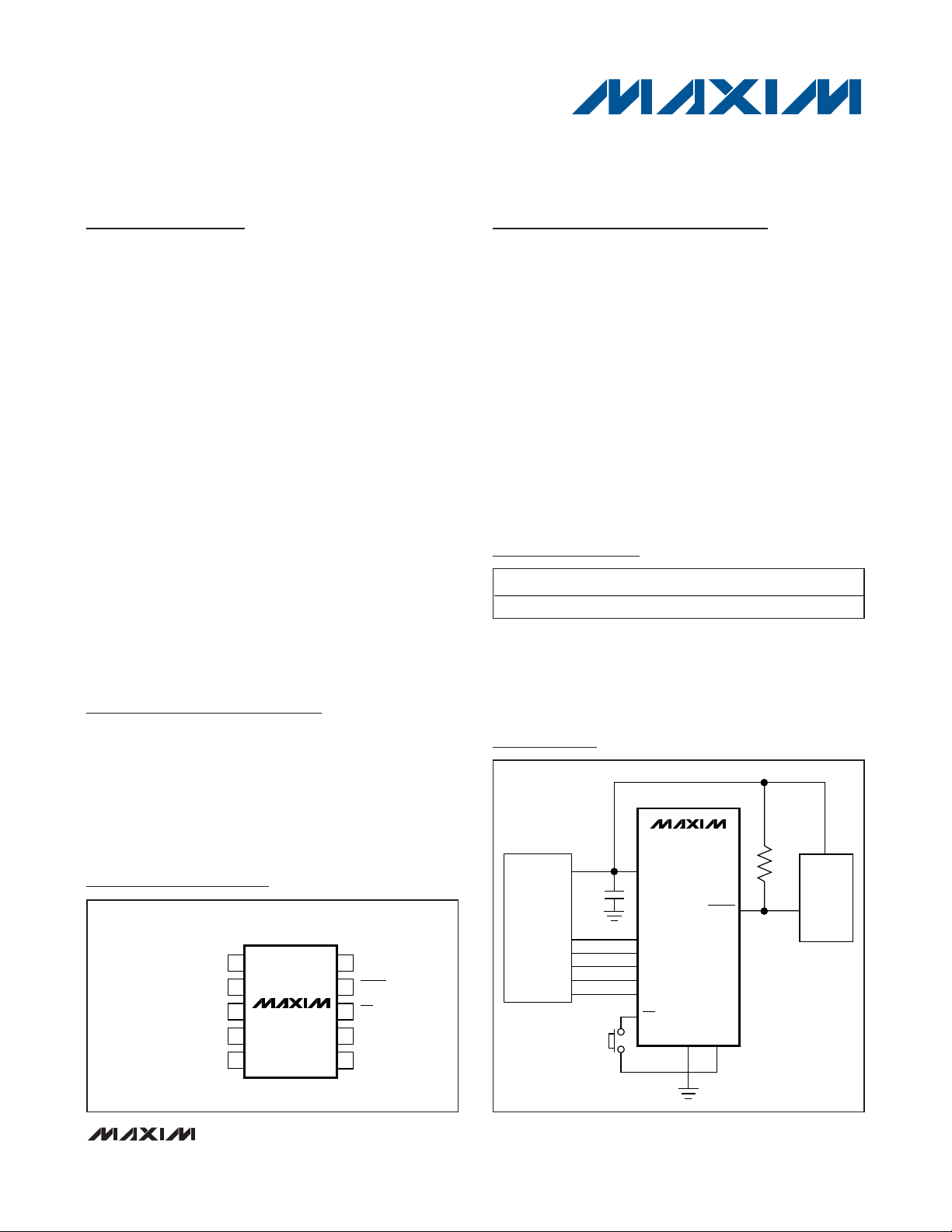
Pin Configuration
Ordering Information
MAX16055
µP
RESET
V
CC
10kΩ
IN2
MR
GND
TOL
MONITORED
SUPPLIES
IN1
0.1µF
IN3
IN4
IN5
IN6
Typical Operating Circuit
19-4411; Rev 0; 1/09
For pricing, delivery, and ordering information, please contact Maxim Direct at 1-888-629-4642,
or visit Maxim’s website at www.maxim-ic.com.
+
Denotes a lead(Pb)-free/RoHS-compliant package.
*
Insert the desired threshold option letter from the Selector
Guide into the blank to complete the part number. Contact factory
for availability.
PART TEMP RANGE
PIN-PACKAGE
-40°C to +125°C 10 µMAX
Telecommunications
High-End Printers
Desktop and Notebook
Computers
Data Storage Equipment
Networking Equipment
Industrial Equipment
Set-Top Boxes
Servers/Workstations
µMAX is a registered trademark of Maxim Integrated Products, Inc.
MAX16055_AUB+*
TOP VIEW
IN1
1 +
2
3
4
5
MAX16055
µMAX
IN2
IN3
GND
10
RESET
9
MR
8
TOLIN4
7
6
IN6IN5
Page 2
MAX16055
Ultra-Small, Hex Voltage,
Microprocessor Supervisor
2 _______________________________________________________________________________________
ABSOLUTE MAXIMUM RATINGS
ELECTRICAL CHARACTERISTICS
(V
IN1
= 1V to 5.5V, TA= -40°C to +125°C, unless otherwise noted. Typical values are at V
IN1
= 3.3V, TA= +25°C.) (Note 1)
Stresses beyond those listed under “Absolute Maximum Ratings” may cause permanent damage to the device. These are stress ratings only, and functional
operation of the device at these or any other conditions beyond those indicated in the operational sections of the specifications is not implied. Exposure to
absolute maximum rating conditions for extended periods may affect device reliability.
RESET, TOL, MR, IN_ to GND ..................................-0.3V to +6V
Input/Output Current (all pins) ............................................20mA
Continuous Power Dissipation (TA= +70°C)
10-Pin µMAX (derate 5.6mW/°C above +70°C) ...........444mW
Operating Temperature Range .........................-40°C to +125°C
Storage Temperature Range .............................-65°C to +150°C
Junction Temperature......................................................+150°C
Lead Temperature (soldering, 10s) .................................+300°C
Operating Voltage Range V
Input Current (Note 3) I
Threshold Voltage V
PARAMETER SYMBOL CONDITIONS MIN TYP MAX UNIT
IN1
IN_
TH
(Note 2) 1.0 5.5 V
V
= nominal input voltage (for IN2–IN6;
IN_
3.3V, 3.0V, 2.5V, 1.8V, 1.5V, 1.2V, 1.1V,
1.0V, 0.9V supplies)
V
= nominal input voltage (for +3.3V IN1
IN1
supply)
V
= 0 to 0.5V or V
IN_
thresholds)
V
decreasing
IN_
(for adjustable
ADJ
3.3V, TOL = GND 3.00 3.08 3.15
3.3V, TOL = V
3.0V, TOL = GND 2.70 2.78 2.85
3.0V , TOL = V
2.5V, TOL = GND 2.25 2.32 2.38
2.5V, TOL = V
1.8V, TOL = GND 1.62 1.67 1.71
1.8V, TOL = V
1.5V, TOL = GND 1.355 1.389 1.425
1.5V, TOL = V
1.2V, TOL = GND 1.084 1.112 1.140
1.2V, TOL = V
1.1V, TOL = GND 0.993 1.019 1.045
1.1V, TOL = V
1.0V, TOL = GND 0.903 0.926 0.95
1.0V, TOL = V
0.9V , TOL = GND 0.813 0.834 0.855
0.9V, TOL = V
25 40
55 115
-0.1 +0.1
IN1
IN1
IN1
IN1
IN1
IN1
IN1
IN1
2.85 2.93 3.00
2.55 2.63 2.70
IN1
2.13 2.19 2.25
1.53 1.58 1.62
1.283 1.316 1.350
1.027 1.053 1.08
0.941 0.965 0.99
0.856 0.878 0.90
0.770 0.790 0.810
µA
V
Page 3
MAX16055
Ultra-Small, Hex Voltage,
Microprocessor Supervisor
_______________________________________________________________________________________ 3
Note 1: 100% production tested at TA= +25°C. Limits over temperature guaranteed by design.
Note 2: The devices are powered from IN1.
Note 3: Monitored IN1 voltage is also the device power supply.
Note 4: RESET output is guaranteed to be in the correct state for IN1 or IN2 falling down to 1V.
ELECTRICAL CHARACTERISTICS (continued)
(V
IN1
= 1V to 5.5V, TA= -40°C to +125°C, unless otherwise noted. Typical values are at V
IN1
= 3.3V, TA= +25°C.) (Note 1)
PARAMETER SYMBOL CONDITIONS MIN TYP MAX UNIT
Adjustable Threshold V
Reset Threshold Hysteresis V
Reset Threshold Temperature
Coefficient
IN_ to Reset Delay t
Reset Timeout Period t
RESET Output Low (Note 4) V
RESET Output High V
RESET Output High Source
Current
TOL Input Current TOL = IN1 100 nA
MR, TOL Input Voltage Low V
MR, TOL Input Voltage High V
MR Minimum Pulse Width 1µs
MR Glitch Rejection 100 ns
MR-to-RESET Delay 200 ns
MR Pullup Resistance 10 20 33 kΩ
TH
HYST
RD
RP
OL
OH
I
OH
IL
IH
V
decreasing
IN_
V
increasing relative to V
IN_
V
falling at 10mV/µs from (VTH + 50mV)
IN_
- 50mV)
to (V
TH
V
= 5V, I
IN1
V
= 2.5V, I
IN1
V
= 1.0V, I
IN1
V
> 2.55V, I
IN1
not asserted
V
> 2.55V, RESET not asserted 70 µA
IN1
= 2mA 0.3
SINK
SINK
SINK
SOURCE
TOL = GND 0.491 0.5 0.506
TOL = V
= 1.2mA 0.4
= 50µA 0.3
= 6µA (min), RESET
CC
decreasing 0.3 %V
IN_
0.465 0.472 0.479
60 ppm/°C
20 µs
140 200 280 ms
0.8 x
V
IN1
0.7 x
V
IN1
0.3 x
V
IN1
V
V
V
V
V
TH
Page 4

MAX16055
Ultra-Small, Hex Voltage,
Microprocessor Supervisor
4 _______________________________________________________________________________________
Typical Operating Characteristics
(V
IN1
= 3.3V, TA= +25°C, unless otherwise noted.)
IN1 INPUT CURRENT
vs. TEMPERATURE
MAX16055 toc01
TEMPERATURE (°C)
IN1 INPUT CURRENT (µA)
1109565 80-10 5 20 35 50-25
44
42
46
48
50
52
54
56
58
60
62
64
66
68
70
40
-40 125
IN1 INPUT CURRENT
vs. IN1 VOLTAGE
MAX16055 toc02
IN1 VOLTAGE (V)
IN1 INPUT CURRENT (µA)
5.04.50.5 1.0 1.5 2.5 3.0 3.52.0 4.0
10
20
30
40
50
60
70
80
0
0 5.5
NORMALIZED THRESHOLD ERROR
vs. TEMPERATURE
MAX16055 toc03
TEMPERATURE (°C)
NORMALIZED THRESHOLD ERROR (%)
95805065
-10 5 20 35-25
-0.8
-0.6
-0.4
-0.2
0
0.2
0.4
0.6
0.8
1.0
-1.0
-40
125
110
MAXIMUM IN_ TRANSIENT DURATION
vs. RESET THRESHOLD OVERDRIVE
MAX16055 toc04
IN_ OVERDRIVE (mV)
MAXIMUM IN_ TRANSIENT DURATION (µs)
900800100 200 300 500 600400 700
10
20
30
40
50
60
70
80
0
0 1000
RESET
ASSERTS ABOVE THIS LINE
RESET PROPAGATION DELAY
vs. RESET THRESHOLD OVERDRIVE
(IN_ DECREASING)
MAX16055 toc05
IN_ OVERDRIVE (mV)
RESET PROPAGATION DELAY (µs)
900800600 700200 300 400 500100
10
20
30
40
50
60
70
80
90
100
0
0 1000
RESET PULLUP AND PULLDOWN
RESPONSE (C
L
= 47pF)
MAX16055 toc06
IN_
100mV/div
AC-COUPLED
RESET
2V/div
20µs/div
RESET TIMEOUT PERIOD
vs. TEMPERATURE
MAX16055 toc07
RESET THRESHOLD (ms)
192
194
196
198
200
202
204
206
208
210
190
TEMPERATURE (°C)
1109580655035205-10-25-40 125
V
IN_
= 3.3V
MR-TO-RESET PROPAGATION DELAY
vs. TEMPERATURE
MAX16055 toc08
TEMPERATURE (°C)
MR-TO-RESET DELAY (ns)
120
110
150
140
130
170
160
200
190
180
210
100
1109580655035205-10-25-40 125
V
IN_
= 3.3V
Page 5

RESET TIMEOUT DELAY
MAX16055 toc09
IN_
1V/div
RESET
1V/div
40ms/div
MR-TO-RESET PROPAGATION DELAY
MAX16055 toc10
MR
2V/div
RESET
2V/div
40ns/div
VIN = 3.3V
MAX16055
Ultra-Small, Hex Voltage,
Microprocessor Supervisor
_______________________________________________________________________________________ 5
Typical Operating Characteristics (continued)
(V
IN1
= 3.3V, TA= +25°C, unless otherwise noted.)
Pin Description
PIN NAME FUNCTION
1 IN1
2 IN2 Voltage Input 2. See the Selector Guide for voltage threshold. Keep IN1 or IN2 > 1V to ensure RESET is valid.
3 IN3 Voltage Input 3. See the Selector Guide for voltage threshold.
4 IN4 Voltage Input 4. See the Selector Guide for voltage threshold.
5 IN5 Voltage Input 5. See the Selector Guide for voltage threshold.
6 IN6 Voltage Input 6. See the Selector Guide for voltage threshold.
7 TOL
8 MR
9 RESET
10 GND Ground
Voltage Input 1. IN1 is the power-supply input and voltage monitoring input for the device. Connect a 0.1µF
bypass capacitor from IN1 to GND. Keep IN1 or IN2 > 1V to ensure RESET is valid.
Threshold Tolerance Input. Connect TOL to GND to select thresholds 5% below nominal. Connect TOL to IN1
to select thresholds 10% below nominal.
Active-Low Manual-Reset Input. When MR is low, RESET goes low and remains asserted for the reset timeout
period after MR is pulled high. MR is internally pulled high by a 20kΩ pullup resistor to IN1.
Active-Low Reset Output. RESET goes low when any input (IN_) goes below the specified threshold. After all
inputs rise above the specified threshold voltages, RESET remains low for 140ms (min) before going high.
The open-drain RESET output features a weak (70µA) internal pullup to IN1.
Page 6

MAX16055
Ultra-Small, Hex Voltage,
Microprocessor Supervisor
6 _______________________________________________________________________________________
Detailed Description
The MAX16055 hex voltage µP supervisory circuit maintains system integrity in multisupply systems (Figure 1).
The MAX16055 offers accurate, factory-fixed undervoltage threshold options for monitoring very low voltages.
The MAX16055 also offers one to five adjustable thresholds for monitoring voltages down to 0.5V. See the
Selector Guide
for the available threshold options.
The MAX16055 includes an accurate voltage reference,
precision comparators, and a series of accurate internal
resistor-divider networks to set the factory-fixed reset
threshold options for monitoring 3.3V, 3.0V, 2.5V, 1.8V,
1.5V, 1.2V, 1.1V, 1.0V, or 0.9V supplies. The resistor
networks scale the specified IN_ threshold voltages to
match the internal reference voltage. Adjustable threshold options allow the monitored voltage to be connected
to the input of the internal comparator. Use an external
voltage-divider to set the threshold voltage.
Figure 1. Functional Diagram
IN1
3.3V
IN2
ADJ
IN3
ADJ
IN4
1.8V
IN5
ADJ
ALL DEVICES ARE POWERED FROM IN1 (3.3V/2.5V); RESET IS VALID IF V
IN1
OR V
TIMEOUT
(200ms)
UVLO
IS GREATER THAN 1V
IN2
PULLUP
IN2
IN1
70µA
RESET
IN6
ADJ
IN1
TOL
MR
REF
MAX16055C
Page 7

The MAX16055 is immune to short IN_ transients. Each
of the internal comparators provides a typical hysteresis of 0.3% with respect to the reset threshold. This
built-in hysteresis improves the monitor’s immunity to
ambient noise without significantly reducing threshold
accuracy. See the
Typical Operating Characteristics
for
a glitch immunity graph labeled Maximum IN_ Transient
Duration vs. Reset Threshold Overdrive.
Reset Output
The MAX16055 RESET output asserts low when any
monitored IN_ voltage drops below the specified reset
threshold. RESET remains low for the reset timeout period of 140ms (min) after all inputs rise above the
respective thresholds (Figure 2). The RESET output is
open drain with a weak internal pullup to the monitored
IN1 supply (70µA typ). For many applications, no external pullup resistor is required to interface with other
logic devices. Apply an external pullup resistor to any
voltage from 0 to 5.5V when interfacing to different
logic-supply voltages (Figure 3). Internal circuitry prevents reverse current flow from the external pullup voltage into the RESET output when RESET is not asserted.
RESET asserts low upon power-up. After all IN_ inputs
rise above the respective threshold voltages, RESET
remains low for the reset timeout period (Figure 4)
before going high.
IN1 powers the MAX16055 and is also a monitored voltage. When any monitored supply drops below the
threshold voltage, RESET asserts low and remains low
while either IN1 or IN2 is above 1.0V.
Adjustable Thresholds
The MAX16055 includes monitor options with
adjustable reset thresholds. The threshold voltage at
each adjustable IN_ input is typically 0.5V. To monitor a
voltage higher than 0.5V, connect a resistor-divider network to the circuit as shown in Figure 5:
V
INTH
= 0.5V x (R1 + R2)/R2
Therefore:
R1 = R2 ((V
INTH
/0.5V) - 1)
Use high valued resistors (~ 100kΩ) to minimize current
through the external resistors. Use lower valued resistors for greater accuracy. The MAX16055 includes an
internal voltage clamp (1.5V typ) at each of the
adjustable voltage inputs. An input voltage higher than
1.5V induces a higher input current.
MAX16055
Ultra-Small, Hex Voltage,
Microprocessor Supervisor
_______________________________________________________________________________________ 7
Figure 2. RESET Output Timing Diagram
Figure 3. Interfacing with External Logic-Supply Voltage
IN_
V
TH_
RESET
10%
t
RD
RESET
+5V
V
CC
µP
GND
+3.3V
V
+ V
HYST
90%
IN1
10kΩ
RESET
MAX16055
GND
TH_
t
RP
Page 8

Manual-Reset Input (MR)
Many µP-based products require manual-reset capability. A logic-low on MR asserts RESET low. RESET
remains asserted while MR is low, and during the reset
timeout period (140ms, min) after MR returns high. The
MR input has an internal 20kΩ pullup resistor to IN1.
Connect a normally open momentary switch from MR to
GND to create a manual-reset function. Connect a
0.1µF capacitor from MR to GND to provide additional
noise immunity when driving MR from long cables or
when the device is used in a noisy environment.
Tolerance (TOL)
The MAX16055 features an adjustable threshold tolerance. Connect TOL to GND to set the threshold voltages 5% below the nominal value. Connect TOL to IN1
to set the threshold voltages 10% below the nominal
value. See the
Electrical Characteristics
table. Do not
leave TOL unconnected.
Applications Information
Unused Inputs
Connect unused monitor inputs to a supply voltage
higher than the specified threshold voltage. Connect a
100kΩ resistor between an unused adjustable input
and IN1 to limit the bias current. Use IN1 for normal
operation (device power supply). Do not connect
unused monitor inputs to ground. Do not leave unused
monitor inputs unconnected.
Reset Output Pullup Resistor
When connecting a pullup resistor from RESET to a
voltage rail lower than the voltage on IN1, the internal
70µA pullup current flows through the pullup resistor,
causing the voltage at RESET to be higher than the voltage rail when RESET is deasserted. Ensure that the
value of the pullup resistor is low enough that the voltage rise does not cause problems.
Power-Supply Bypassing and Grounding
IN1 powers the MAX16055. Connect a 0.1µF bypass
capacitor from IN1 to ground. All monitored inputs are
immune to short supply transients. Add bypass capacitors from IN2–IN6 to GND to improve noise immunity.
MAX16055
Ultra-Small, Hex Voltage,
Microprocessor Supervisor
8 _______________________________________________________________________________________
Figure 4. RESET Output with Various Input Voltages
Figure 5. Setting the Adjustable Threshold
V
IN1
V
IN2
V
IN3
V
IN4
V
IN5
V
IN6
t
BEGINS
RP
WHEN THE LAST
SUPPLY EXCEEDS
+ V
ITS V
TH
HYST
RESET
V
+ V
TH
HYST
t
RP
V
INTH
MAX16055
R1
R2
V
TH
R1 = R2
V
INTH
(
-1
V
TH
)
Page 9

MAX16055
Ultra-Small, Hex Voltage,
Microprocessor Supervisor
Maxim cannot assume responsibility for use of any circuitry other than circuitry entirely embodied in a Maxim product. No circuit patent licenses are
implied. Maxim reserves the right to change the circuitry and specifications without notice at any time.
Maxim Integrated Products, 120 San Gabriel Drive, Sunnyvale, CA 94086 408-737-7600 _____________________
9
© 2009 Maxim Integrated Products is a registered trademark of Maxim Integrated Products, Inc.
Chip Information
PROCESS: BiCMOS
Selector Guide
Package Information
For the latest package outline information and land patterns, go
to www.maxim-ic.com/packages
.
PACKAGE TYPE PACKAGE CODE DOCUMENT NO.
10 µMAX U10+2
21-0061
*
Adjustable voltage is based on the 0.5V internal threshold. External threshold voltage can be set using an external resistor-divider.
(V
ADJ
= 0.500V typ).
PART*
(SUFFIX IN BOLD)
MAX16055A 3.3 2.5 1.5 1.8 1.2 0.9
MAX16055B 3.3 3.0 1.8 1.5 1.1 1.0
MAX16055C 3.3 ADJ ADJ 1.8 ADJ ADJ
MAX16055D 3.3 ADJ 1.5 ADJ ADJ ADJ
MAX16055E 3.3 2.5 ADJ 1.8 ADJ ADJ
MAX16055F 3.3 2.5 1.5 ADJ ADJ ADJ
MAX16055G 3.3 2.5 ADJ ADJ ADJ ADJ
MAX16055H 3.3 ADJ ADJ ADJ ADJ ADJ
MAX16055I 2.5 ADJ ADJ ADJ ADJ ADJ
MAX16055J 3.3 3.3 2.5 1.2 1.5 1.2
IN1 IN2 IN3 IN4 IN5 IN6
NOMINAL INPUT VOLTAGE (V)
 Loading...