

Page 1
General Description
The MAX16033–MAX16040 supervisory circuits reduce
the complexity and number of components required for
power-supply monitoring and battery control functions
in microprocessor (µP) systems. The devices significantly improve system reliability and accuracy compared to other ICs or discrete components. The
MAX16033–MAX16040 provide µP reset, backup-battery switchover, power-fail warning, watchdog, and
chip-enable gating features.
The MAX16033–MAX16040 operate from supply voltages up to 5.5V. The factory-set reset threshold voltage
ranges from 2.32V to 4.63V. The devices feature a manual-reset input (MAX16033/MAX16037), a watchdog
timer input (MAX16034/MAX16038), a battery-on output
(MAX16035/MAX16039), an auxiliary adjustable reset
input (MAX16036/MAX16040), and chip-enable gating
(MAX16033–MAX16036). Each device includes a
power-fail comparator and offers an active-low pushpull reset or an active-low open-drain reset.
The MAX16033–MAX16040 are available in 2mm x
2mm, 8-pin or 10-pin µDFN packages and are fully
specified from -40°C to +85°C.
Applications
Features
♦ Low 1.2V Operating Supply Voltage
♦ Precision Monitoring of 5.0V, 3.3V, 3.0V, and 2.5V
Power-Supply Voltages
♦ Independent Power-Fail Comparator
♦ Debounced Manual-Reset Input
♦ Watchdog Timer, 1.6s Timeout
♦ Battery-On Output Indicator
♦ Auxiliary User-Adjustable RESETIN
♦ Low 13µA Quiescent Supply Current
♦ Two Available Output Structures:
Active-Low Push-Pull Reset
Active-Low Open-Drain Reset
♦ Active-Low Reset Valid Down to 1.2V
♦ Power-Supply Transient Immunity
♦ 140ms (min) Reset Timeout Period
♦ Small 2mm x 2mm, 8-Pin and 10-Pin µDFN
Packages
MAX16033–MAX16040
Low-Power Battery Backup
Circuits in Small µDFN Packages
________________________________________________________________
Maxim Integrated Products
1
19-0882; Rev 0; 7/07
For pricing, delivery, and ordering information, please contact Maxim Direct at 1-888-629-4642,
or visit Maxim’s website at www.maxim-ic.com.
Ordering Information continued on last page.
*
These parts offer a choice of reset threshold voltages. From the
Reset Threshold Ranges table, insert the desired threshold voltage code in the blank to complete the part number. See Selector
Guide for a listing of device features.
+
Denotes a lead-free package.
T
= Tape and reel.
Pin Configurations and Typical Operating Circuit appear at
end of data sheet.
Ordering Information
Note: Replace “_” with L for push-pull or P for open-drain RESET and PFO outputs.
Selector Guide
Portable/BatteryPowered Equipment
POS Equipment
Critical µP/µC Power
Monitoring
Set-Top Boxes
Controllers
Computers
Fax Machines
Industrial Control
Real-Time Clocks
Intelligent Instrument
PART* TEMP RANGE
MAX16033LLB_ _+T -40°C to +85°C 10 µDFN-10 L1022-1
MAX16033PLB_ _+T -40°C to +85°C 10 µDFN-10 L1022-1
MAX16034LLB_ _+T -40°C to +85°C 10 µDFN-10 L1022-1
MAX16034PLB_ _+T -40°C to +85°C 10 µDFN-10 L1022-1
PINPACKAGE
PKG
CODE
PART MR WATCHDOG BATTON RESETIN
MAX16033_ ✓✓✓10 µDFN-10
MAX16034_ ✓✓✓10 µDFN-10
MAX16035_ ✓✓✓10 µDFN-10
MAX16036_ ✓✓ ✓10 µDFN-10
MAX16037_ ✓ ✓ 8 µDFN-8
MAX16038_ ✓✓8 µDFN-8
MAX16039_ ✓✓8 µDFN-8
MAX16040_ ✓✓8 µDFN-8
CEIN/CEOU
PFI, PFO PIN-PACKAGE
Page 2

MAX16033–MAX16040
Low-Power Battery Backup
Circuits in Small µDFN Packages
2 _______________________________________________________________________________________
ABSOLUTE MAXIMUM RATINGS
ELECTRICAL CHARACTERISTICS
(VCC= 2.25V to 5.5V, V
BATT
= 3V, RESET not asserted, TA= -40°C to +85°C, unless otherwise noted. Typical values are at TA=
+25°C.) (Note 1)
Stresses beyond those listed under “Absolute Maximum Ratings” may cause permanent damage to the device. These are stress ratings only, and functional
operation of the device at these or any other conditions beyond those indicated in the operational sections of the specifications is not implied. Exposure to
absolute maximum rating conditions for extended periods may affect device reliability.
Terminal Voltages (with respect to GND)
V
CC,
BATT, OUT .......................................................-0.3V to +6V
RESET (open drain), PFO (open drain) ....................-0.3V to +6V
RESET (push-pull), PFO (push-pull), BATTON, RESETIN, WDI
MR, CEIN, CEOUT, PFI ............................-0.3V to (V
OUT
+ 0.3V)
Input Current
V
CC
Peak..............................................................................1A
V
CC
Continuous ............................................................250mA
BATT Peak ....................................................................250mA
BATT Continuous ............................................................40mA
GND ................................................................................75mA
Output Current
OUT ..................................Short-Circuit Protected for up to 5s
RESET, BATTON .............................................................20mA
Continuous Power Dissipation (T
A
= +70°C)
8-Pin µDFN (derate 4.8mW/°C above +70°C) ..........380.6mW
10-Pin µDFN (derate 5mW/°C above +70°C) ...........402.8mW
Operating Temperature Range ...........................-40°C to +85°C
Storage Temperature Range .............................-65°C to +150°C
Lead Temperature (soldering, 10s) .................................+300°C
Operating Voltage Range VCC, V
Supply Current in Battery
Backup Mode
BATT Standby Current (Note 3) I
Output Voltage in Battery
Backup Mode
Battery-Switchover Threshold V
PARAMETER SYMBOL CONDITIONS MIN TYP MAX UNITS
No load (Note 2) 0 5.5 V
BATT
CC
BATT
ON
V
OUT
SW
No load, VCC > V
= 2.8V,
V
BATT
= 0V,
V
CC
excluding I
(V
BATT
< 5.5V
VCC = 4.75V, VCC > VTH, I
VCC = 3.15V, VCC > VTH, I
VCC = 2.5V, VCC > VTH, I
V
BATT
V
BATT
V
BATT
VCC - V
OUT
+ 0.2V) < V
= 4.50V, VCC = 0V, I
= 3.15V, VCC = 0V, I
= 2.5V, VCC = 0V, I
BATT, VCC
VCC = 2.8V 13 30
VCC = 3.6V 16 35Supply Current I
TH
VCC = 5.5V 22 50
TA = +25°C 1
TA = -40°C to +85°C 2
TA = +25°C -0.1 +0.02
CC
T
= -40°C to +85°C -0.3 +0.02
A
= 150mA 3.1
OUT
= 65mA 3.7VCC to OUT On-Resistance R
OUT
= 25mA 4.6
OUT
V
BATT
- 0.2
V
BATT
- 0.15
V
BATT
- 0.15
< V
TH
= 20mA
OUT
= 10mA
OUT
= 5mA
OUT
VCC rising 0
VCC falling -40
µA
µA
µA
Ω
V
mV
Page 3
MAX16033–MAX16040
Low-Power Battery Backup
Circuits in Small µDFN Packages
_______________________________________________________________________________________ 3
ELECTRICAL CHARACTERISTICS (continued)
(VCC= 2.25V to 5.5V, V
BATT
= 3V, RESET not asserted, TA= -40°C to +85°C, unless otherwise noted. Typical values are at TA=
+25°C.) (Note 1)
)
PARAMETER SYMBOL CONDITIONS MIN TYP MAX UNITS
RESET OUTPUT
MAX160_ _ _L_46 4.50 4.63 4.75
MAX160_ _ _L_44 4.25 4.38 4.50
Reset Threshold V
VCC Falling Reset Delay VCC falling at 10V/ms 25 µs
Reset Active Timeout Period t
RESET Output Low Voltage V
RESET Output High Voltage V
RESET Output Leakage
Current
POWER-FAIL COMPARATOR
PFI Input Threshold V
PFI Hysteresis 1%
PFI Input Current V
PFO Output Low Voltage V
PFO Output High Voltage V
PFO Leakage Current
PFO Delay Time V
MANUAL RESET (MAX16033/MAX16037)
MR Input Voltage
Pullup Resistance to V
Minimum Pulse Width 1µs
Glitch Immunity VCC = 3.3V 100 ns
MR to Reset Delay 120 ns
CC
I
LKG
V
V
TH
RP
OL
OH
PFI
OL
OH
IL
IH
MAX160_ _ _L_31 3.00 3.08 3.15
MAX160_ _ _L_29 2.85 2.93 3.00
MAX160_ _ _L_26 2.55 2.63 2.70
MAX160_ _ _L_23 2.25 2.32 2.38
140 280 ms
I
= 1.6mA, VCC > 2.1V 0.3
RESET asserted
MAX160_ _L only (push-pull), RESET not
asserted, I
MAX160_ _P only (open drain), not asserted 1 µA
V
PFI
PFI
O utp ut asser ted
MAX160_ _L only (push-pull), VCC > V
I
SOURCE
MAX160_ _P only (open drain), V
not asserted
PFI
SOURCE
falling 1.185 1.235 1.285 V
= 0V or V
= 500µA, output not asserted
+ 100mV to V
SINK
= 100µA, VCC > 1.2V 0.4
I
SINK
0.8 x
= 500µA, VCC > V
CC
VCC > 2.1V, I
V
> 1.2V, I
CC
- 100mV 4 µs
PFI
TH(MAX
= 1.6mA 0.3
SINK
= 100µA 0.4
SINK
TH(MAX),
= 5.5V,
PFO
V
CC
-100 +100 nA
0.8 x
V
CC
0.7 x
V
CC
20 165 kΩ
1µA
0.3 x
V
CC
V
V
V
V
V
V
Page 4
MAX16033–MAX16040
Low-Power Battery Backup
Circuits in Small µDFN Packages
4 _______________________________________________________________________________________
Note 1: All devices are 100% production tested at TA= +25°C. All overtemperature limits are guaranteed by design.
Note 2: V
BATT
can be 0V any time, or VCCcan go down to 0V if V
BATT
is active (except at startup).
Note 3: Positive current flows into BATT.
Note 4: Guaranteed by design.
ELECTRICAL CHARACTERISTICS (continued)
(VCC= 2.25V to 5.5V, V
BATT
= 3V, RESET not asserted, TA= -40°C to +85°C, unless otherwise noted. Typical values are at TA=
+25°C.) (Note 1)
PARAMETER SYMBOL CONDITIONS MIN TYP MAX UNITS
WATCHDOG (MAX16034/MAX16038)
Watchdog Timeout Period t
M i ni m um WD I Inp ut P ul se W i d th t
WDI Input Voltage
WDI Input Current -1.0 +1.0 µA
BATTON (MAX16035/MAX16039)
Output Voltage V
Output Short-Circuit Current
RESETIN (MAX16036/MAX16040)
RESETIN Threshold V
RESETIN Input Current 0.01 25 nA
RESETIN to Reset Delay (V
CHIP-ENABLE GATING (MAX16033–MAX16036)
CEIN Leakage Current RESET asserted ±1 µA
CEIN to CEOUT Resistance
CEOUT Short-Circuit Current RESET asserted, V
CEIN to CEOUT Propagation
Delay (Note 4)
CEOUT Output-Voltage High
RESET to CEOUT Delay 1µs
WD
WDI
V
V
OL
RTH
(Note 4) 100 ns
IL
IH
I
= 3.2mA, V
SINK
Sink current, VCC = 5V 60 mA
Source current, V
+ 100mV) to (V
RTH
RESET not asserted, V
V
= VCC / 2, I
CEIN
50Ω source impedance driver,
= 50pF
C
LOAD
VCC = 5V, VCC > V
= 0V, V
V
CC
BATT
= 2.1V 0.4 V
BATT
> 2V 10 30 120 µA
BATT
- 100mV) 1.5 µs
RTH
= V
CC
TH(MAX),
= 10mA
SINK
= 0V 1 2.0 mA
CEOUT
VCC = 4.75V 1.5 7
V
= 3.15V 2 9
CC
SOURCE
SOURCE
= 100µA
= 1µA
BATT
> 2.2V, I
, I
1.00 1.65 2.25 s
0.3 x
V
CC
0.7 x
V
CC
1.185 1.235 1.285 V
100 Ω
0.7 x
V
CC
V
BATT
- 0.1
V
ns
V
Page 5
MAX16033–MAX16040
Low-Power Battery Backup
Circuits in Small µDFN Packages
_______________________________________________________________________________________
5
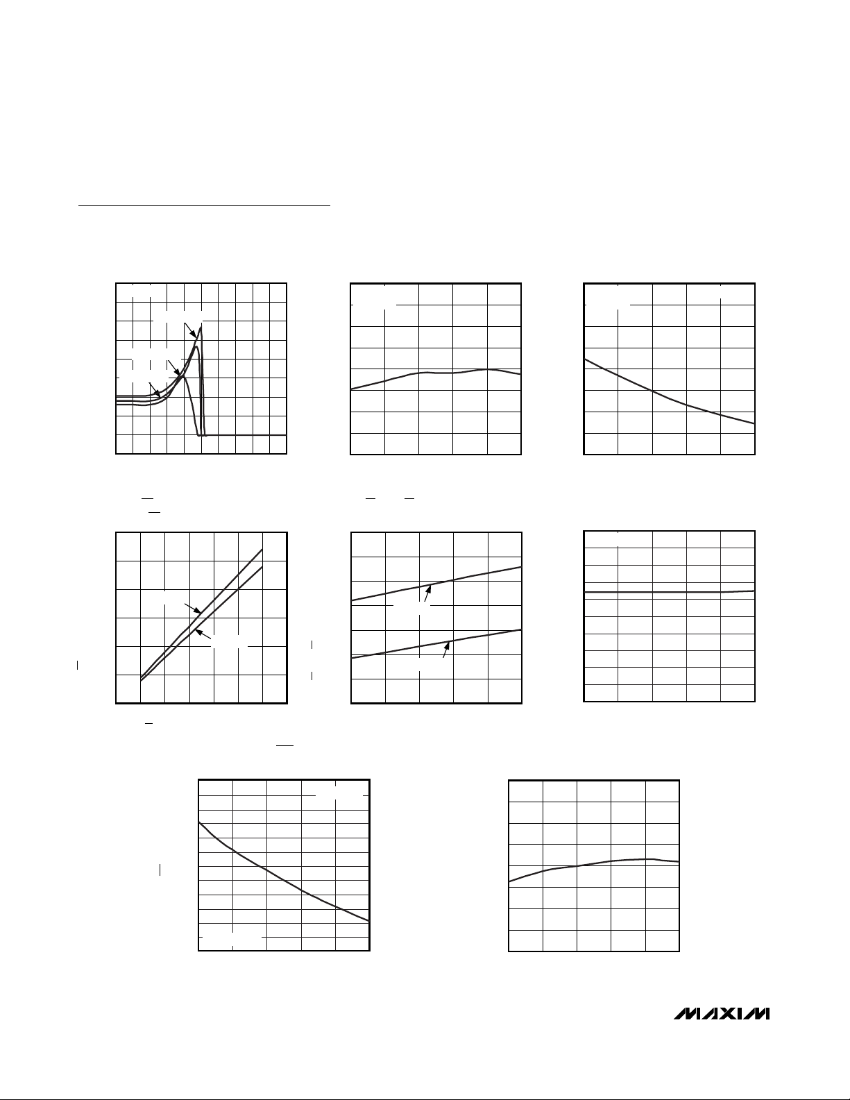
Typical Operating Characteristics
(TA = +25°C, unless otherwise noted.)
SUPPLY CURRENT
vs. TEMPERATURE
20
VCC = 5V
19
18
17
16
15
14
13
SUPPLY CURRENT (µA)
12
11
10
-40 85
TEMPERATURE (°C)
603510-15
VCC-TO-OUT ON-RESISTANCE
vs. TEMPERATURE
1.4
1.2
1.0
0.8
0.6
0.4
-TO-OUT ON-RESISTANCE (Ω)
CC
V
0.2
0
-40 80
VCC = 2.5V
= 25mA
I
OUT
VCC = 3V
= 65mA
I
OUT
TEMPERATURE (°C)
VCC = 4.5V
= 150mA
I
OUT
6550-25 -10 5 20 35
(BACKUP MODE) vs. TEMPERATURE
1.0
0.9
MAX16033 toc01
0.8
0.7
0.6
0.5
0.4
0.3
0.2
BATTERY SUPPLY CURRENT (µA)
0.1
0
-40 85
230
VCC = 5V
225
MAX16033 toc04
220
215
210
205
200
195
RESET TIMEOUT PERIOD (ms)
190
185
180
-40 85
BATTERY SUPPLY CURRENT
V
= 3V
BATT
= 0V
V
CC
TEMPERATURE (°C)
RESET TIMEOUT PERIOD
vs. TEMPERATURE
TEMPERATURE (°C)
BATT-TO-OUT ON-RESISTANCE
1.0
9
MAX16033 toc02
603510-15
MAX16033 toc05
603510-15
8
7
6
5
4
3
2
BATTERY-TO-OUT ON-RESISTANCE (Ω)
1
0
-40 85
120
105
90
75
60
45
30
-TO-RESET PROPAGATION DELAY (µs)
CC
15
V
0
-40 80
vs. TEMPERATURE
VCC = 0V
V
= 2V
BATT
V
= 5V
V
= 3V
BATT
TEMPERATURE (°C)
BATT
603510-15
VCC-TO-RESET PROPAGATION DELAY
vs. TEMPERATURE
VCC FALLING
0.25V/ms
1V/ms
10V/ms
6040-20 0 20
TEMPERATURE (°C)
MAX16033 toc03
MAX16033 toc06
NORMALIZED RESET THRESHOLD
vs. TEMPERATURE
1.003
1.002
1.001
1.000
0.999
0.998
0.997
0.996
0.995
0.994
0.993
NORMALIZED RESET THRESHOLD
0.992
0.991
0.990
-40 80
TEMPERATURE (°C)
MAX16033 toc07
6040200-20
MAXIMUM TRANSIENT DURATION
vs. RESET THRESHOLD OVERDRIVE
300
RESET OCCURS
ABOVE CURVE
250
200
150
100
50
MAXIMUM TRANSIENT DURATION (µs)
0
1 10,000
RESET THRESHOLD OVERDRIVE (VTH - VCC) (mV)
MAX160_ _-46
= 4.63V)
(V
TH
MAX160_ _-29
= 2.93V)
(V
TH
MAX16033 toc08
100010010
Page 6
MAX16033–MAX16040
Low-Power Battery Backup
Circuits in Small µDFN Packages
6 _______________________________________________________________________________________
Typical Operating Characteristics (continued)
(TA = +25°C, unless otherwise noted.)
BATTERY SUPPLY CURRENT
vs. SUPPLY VOLTAGE
MAX16033 toc09
SUPPLY VOLTAGE (V)
BATTERY SUPPLY CURRENT (µA)
4.54.03.0 3.51.0 1.5 2.0 2.50.5
0
0.25
0.50
0.75
1.00
1.25
1.50
1.75
2.00
-0.25
0 5.0
V
BATT
= 2.8V
VTH = 2.93V
V
BATT
= 2.5V
V
BATT
= 2.3V
RESETIN THRESHOLD
vs. TEMPERATURE
MAX16033 toc10
TEMPERATURE (°C)
RESETIN THRESHOLD (V)
6035-15 10
1.215
1.220
1.225
1.230
1.235
1.240
1.245
1.250
1.210
-40 85
MAX16036/
MAX16040
RESETIN-TO-RESET PROPAGATION
DELAY vs. TEMPERATURE
MAX16033 toc11
TEMPERATURE (°C)
RESETIN-TO-RESET PROPAGATION DELAY (µs)
6035-15 10
1.3
1.5
1.8
2.0
2.3
2.5
2.8
3.0
1.0
-40 85
MAX16036/
MAX16040
VOD = 50mV
CEIN PROPAGATION DELAY
vs. CEOUT LOAD CAPACITANCE
MAX16033 toc12
CEOUT LOAD CAPACITANCE (pF)
CEIN PROPAGATION DELAY (ns)
150125100755025
0.5
1.0
1.5
2.0
2.5
3.0
0
0175
VCC = 3V
VCC = 5V
CEIN TO CEOUT ON-RESISTANCE
vs. TEMPERATURE
MAX16033 toc13
TEMPERATURE (°C)
CEIN TO CEOUT ON-RESISTANCE (Ω)
603510-15
5
10
15
20
25
30
35
0
-40 85
VCC = 3V
VCC = 5V
PFI-TO-PFO DELAY
vs. TEMPERATURE
MAX16033 toc15
TEMPERATURE (°C)
PFI-TO-PFO DELAY (µs)
603510-15
3.25
3.50
4.00
3.75
4.25
4.50
2.25
2.75
2.50
3.00
4.75
5.00
2.00
-40 85
VOD = 30mV
FALLING EDGE
PFI THRESHOLD
vs. TEMPERATURE
MAX16033 toc16
TEMPERATURE (°C)
PFI THRESHOLD (V)
6035-15 10
1.215
1.220
1.225
1.230
1.235
1.240
1.245
1.250
1.210
-40 85
WATCHDOG TIMEOUT PERIOD
vs. TEMPERATURE
MAX16033 toc14
TEMPERATURE (°C)
WATCHDOG TIMEOUT PERIOD (s)
603510-15
1.4
1.5
1.6
1.7
1.8
1.1
1.2
1.3
1.9
2.0
1.0
-40 85
VCC = 5V
Page 7
MAX16033–MAX16040
Low-Power Battery Backup
Circuits in Small µDFN Packages
_______________________________________________________________________________________ 7
Pin Description
PIN
MAX16033–
MAX16036
(10-pin µDFN)
11RESET
2—CEIN
3 2 PFI Power-Fail Input. PFO goes low when V
4 3 GND Ground
54
MAX16037–
MAX16040
(8-pin µDFN)
NAME FUNCTION
Active-Low Reset Output. RESET remains low when V
MR
WDI
BATTON
RESETIN
threshold (V
pulses when the internal watchdog times out. RESET remains low for the reset
timeout period (t
input goes from low to high, after RESETIN goes high, or after the watchdog triggers
a reset event. The MAX160_ _L is an active-low push-pull output, while the
MAX160_ _P is an active-low open-drain output.
Chip-Enable Input. The input to the chip-enable gating circuit. Connect to GND or
OUT if not used.
Manual-Reset Input (MAX16033/MAX16037). Driving MR low asserts RESET. RESET
remains asserted as long as MR is low and for the reset timeout period (t
MR transitions from low to high. Leave unconnected, or connect to V
MR has an internal 20kΩ pullup to V
Watchdog Input (MAX16034/MAX16038). If WDI remains high or low for longer than
the watchdog timeout period (t
pulse is triggered for the reset timeout period (t
whenever RESET asserts or whenever WDI sees a rising or falling edge (Figure 2).
Battery-On Output (MAX16035/MAX16039). BATTON goes high during battery
backup mode.
Reset Input (MAX16036/MAX16040). When RESETIN falls below 1.235V, RESET
asserts. RESET remains asserted as long as RESETIN is low and for at least t
after RESETIN goes high.
), the manual-reset input is low, or RESETIN is low. It asserts low in
TH
) after VCC rises above the reset threshold, after the manual-reset
RP
is below the reset
CC
falls below 1.235V.
PFI
) after
RP
if not used.
.
CC
), the internal watchdog timer runs out and a reset
WD
). The internal watchdog clears
RP
CC
RP
Active-Low Power-Fail Output. PFO goes low when V
65PFO
76V
8 7 OUT
9 8 BATT
10 — CEOUT
CC
stays low until V
the reset threshold voltage.
Supply Voltage, 1.2V to 5.5V
Output. OUT sources from V
V
CC
Backup Battery Input. When V
BATT if V
switches to V
slowly.
Chip-Enable Output. CEOUT goes low only when CEIN is low and reset is not
asserted. When CEOUT is disconnected from CEIN, CEOUT is actively pulled up to
OUT.
falls below 1.235V. PFO
goes above 1.235V. PFO also goes low when VCC falls below
PFI
when RESET is not asserted and from the greater of
or BATT when VCC is below the reset threshold voltage.
is 40mV greater than VCC. When VCC rises above V
BATT
. The 40mV hysteresis prevents repeated switching if VCC falls
CC
CC
falls below the reset threshold, OUT switches to
CC
PFI
BATT
, OUT
Page 8

MAX16033–MAX16040
Low-Power Battery Backup
Circuits in Small µDFN Packages
8 _______________________________________________________________________________________
Functional Diagram
BATTON (MAX16035/MAX16039 ONLY)
1.235V
V
CC
BATT
(MAX16033–MAX16036 ONLY)
CEIN
CHIP-ENABLE
OUTPUT
CONTROL
MAX16033–
MAX16040
OUT
CEOUT
(MAX16033/MAX16037 ONLY)
(MAX16034/MAX16038 ONLY)
(MAX16036/MAX16040 ONLY)
WDI
RESETIN
MR
WATCHDOG
TRANSITION
DETECTOR
1.235V
GND
RESET
GENERATOR
WATCHDOG
TIMER
RESET
PFO
1.235V
PFI
Page 9

MAX16033–MAX16040
Low-Power Battery Backup
Circuits in Small µDFN Packages
_______________________________________________________________________________________ 9
Detailed Description
The
Typical Operating Circuit
shows a typical connection for the MAX16033–MAX16040. OUT powers the
static random-access memory (SRAM). If V
CC
is
greater than the reset threshold (VTH), or if VCCis lower
than VTHbut higher than V
BATT
, VCCis connected to
OUT. If V
CC
is lower than VTHand VCCis less than
V
BATT
, BATT is connected to OUT. OUT supplies up to
200mA from VCC. In battery-backup mode, an internal
MOSFET connects the backup battery to OUT. The onresistance of the MOSFET is a function of the backupbattery voltage and temperature and is shown in the
BATT-to-OUT On-Resistance vs. Temperature graph in
the
Typical Operating Characteristics
.
Chip-Enable Signal Gating
(MAX16033–MAX16036 Only)
The MAX16033–MAX16036 provide internal gating of
chip-enable (CE) signals to prevent erroneous data
from being written to CMOS RAM in the event of a
power failure or brownout condition. During normal
operation, the CE gate is enabled and passes all CE
transitions. When reset asserts, this path becomes
disabled, preventing erroneous data from corrupting
the CMOS RAM. The MAX16033–MAX16036 provide a
series transmission gate from CEIN to CEOUT. A 2ns
(typ) propagation delay from CEIN to CEOUT allows
these devices to be used with most µPs and highspeed DSPs.
When RESET is deasserted, CEIN is connected to
CEOUT through a low on-resistance transmission gate.
If CEIN is high when RESET is asserted, CEOUT
remains high regardless of any subsequent transitions
on CEIN during the reset event.
If CEIN is low when RESET is asserted, CEOUT is held
low for 1µs to allow completion of the read/write operation (Figure 1). After the 1µs delay expires, CEOUT
goes high and stays high regardless of any subsequent
transitions on CEIN during the reset event. When
CEOUT is disconnected from CEIN, CEOUT is actively
pulled up to OUT.
The propagation delay through the chip-enable circuitry depends on both the source impedance of the drive
to CEIN and the capacitive loading at CEOUT. The
chip-enable propagation delay is specified from the
50% point of CEIN to the 50% point of CEOUT, using a
50Ω driver and 50pF load capacitance. Minimize the
capacitive load at CEOUT and use a low output-impedance driver to minimize propagation delay.
In high-impedance mode, the leakage current at CEIN
is ±1µA (max) over temperature. In low-impedance
mode, the impedance of CEIN appears as a 75Ω resistor in series with the load at CEOUT.
Figure 1. RESET and Chip-Enable Timing
V
CC
V
TH
CEIN
CEOUT
RESET-TO-CEOUT DELAY
RESET
PFO
PFI > V
PFI
t
RD
t
RP
t
RD
* IF CEIN GOES HIGH BEFORE RESET ASSERTS,
CEOUT GOES HIGH WITHOUT DELAY AS CEIN GOES HIGH.
*
t
RP
Page 10

MAX16033–MAX16040
Low-Power Battery Backup
Circuits in Small µDFN Packages
10 ______________________________________________________________________________________
Backup Battery Switchover
To preserve the contents of the RAM in a brownout or
power failure, the MAX16033–MAX16040 automatically
switch to back up the battery installed at BATT when
the following two conditions are met:
1) V
CC
falls below the reset threshold voltage.
2) VCCis below V
BATT
.
Table 1 lists the status of the inputs and outputs in battery-backup mode. The devices do not power-up if the
only voltage source is V
BATT
. OUT only powers up from
V
CC
at startup.
Manual-Reset Input
(MAX16033/MAX16037 Only)
Many µP-based products require manual-reset capability, allowing the user or external logic circuitry to initiate
a reset. For the MAX16033/MAX16037, a logic-low on
MR asserts RESET. RESET remains asserted while MR
is low and for a minimum of 140ms (tRP) after it returns
high. MR has an internal 20kΩ (min) pullup resistor to
VCC. This input can be driven from TTL/CMOS logic
outputs or with open-drain/collector outputs. Connect a
normally-open momentary switch from MR to GND to
create a manual-reset function; external debounce circuitry is not required. When driving MR from long
cables or when using the device in a noisy environment, connect a 0.1µF capacitor from MR to GND to
provide additional noise immunity.
Watchdog Input
(MAX16034/MAX16038 Only)
The watchdog monitors µP activity through the watchdog input (WDI). RESET asserts when the µP fails to
toggle WDI. Connect WDI to a bus line or µP I/O line. A
change of state (high to low, low to high, or a minimum
100ns pulse) resets the watchdog timer. If WDI remains
high or low for longer than the watchdog timeout period
(tWD), the internal watchdog timer runs out and triggers
a reset pulse for the reset timeout period (t
RP
). The
internal watchdog timer clears whenever reset is
asserted or whenever WDI sees a rising or falling edge.
If WDI remains in either a high or low state, a reset
pulse periodically asserts after every watchdog timeout
period (t
WD
); see Figure 2.
Table 1. Input and Output Status in
Battery-Backup Mode
Figure 2. MAX16034/MAX16038 Watchdog Timeout Period and
Reset Active Time
PIN STATUS
V
CC
OUT Connected to BATT
BATT
RESET Asserted
BATTON High state
MR, RESETIN,
CEIN, and WDI
CEOUT Connected to OUT
PFO Asserted
Disconnected from OUT
Connected to OUT. Current drawn from the
battery is less than 1µA (at V
excluding I
Inputs ignored
) when VCC = 0V.
OUT
BATT
= 2.8V,
WDI
RESET
t
= WATCHDOG TIMEOUT PERIOD
WD
= RESET TIMEOUT PERIOD
t
RP
t
RP
t
WD
t
WD
t
RP
Page 11

MAX16033–MAX16040
Low-Power Battery Backup
Circuits in Small µDFN Packages
______________________________________________________________________________________ 11
BATTON Indicator
(MAX16035/MAX16039 Only)
BATTON is a push-pull output that asserts high when in
battery-backup mode. BATTON typically sinks 3.2mA
at a 0.4V saturation voltage. In battery-backup mode,
this terminal sources approximately 10µA from OUT.
Use BATTON to indicate battery-switchover status or to
supply base drive to an external pass transistor for
higher current applications (see Figure 3).
RESETIN Comparator
(MAX16036/MAX16040 Only)
An internal 1.235V reference sets the RESETIN threshold voltage. RESET asserts when the voltage at
RESETIN is below 1.235V. Use the RESETIN function to
monitor a secondary power supply.
Use the following equations to set the reset threshold
voltage (V
RTH
) of the secondary power supply (see
Figure 4):
V
RTH
= V
REF
(R1 / R2 + 1)
where V
REF
= 1.235V. To simplify the resistor selection,
choose a value for R2 and calculate R1.
R1 = R2 [(V
RTH
/ V
REF
) - 1]
Since the input current at RESETIN is 25nA (max), large
values (up to 1MΩ) can be used for R2 with no significant loss in accuracy.
Power-Fail Comparator
The MAX16033–MAX16040 issue an interrupt (nonmaskable or regular) to the µP when a power failure occurs.
The power line is monitored by two external resistors connected to the power-fail input (PFI). When the voltage at
PFI falls below 1.235V, the power-fail output (PFO) drives
the processor’s NMI input low. An earlier power-fail warning can be generated if the unregulated DC input of the
regulator is available for monitoring. The MAX16033–
MAX16040 turn off the power-fail comparator and force
PFO low when V
CC
falls below the reset threshold volt-
age (see Figure 1). The MAX160_ _L devices provide
push-pull PFO outputs. The MAX160_ _P devices provide
open-drain PFO outputs.
Figure 3. MAX16035/MAX16039 BATTON Driving an External Pass Transistor
Figure 4. Setting RESETIN Voltage for the
MAX16036/MAX16040
V
CC
V
IN
R1
R2
MAX16036
MAX16040
RESETIN
2.4V TO 5.5V
0.1µF
V
BATTON
CC
BATT
MAX16035
MAX16039
GND
( ) FOR MAX16035 ONLY
OUT
(CEOUT)
(CEIN)
RESET
CE
ADDRESS
DECODE
CMOS RAM
A0–A15
µP
RESET
Page 12

MAX16033–MAX16040
Low-Power Battery Backup
Circuits in Small µDFN Packages
12 ______________________________________________________________________________________
RESET
A µP’s reset input puts the µP in a known state. The
MAX16033–MAX16040 µP supervisory circuits assert a
reset to prevent code-execution errors during powerup, power-down, and brownout conditions. RESET
asserts when V
CC
is below the reset threshold voltage
and for at least 140ms (tRP) after VCCrises above the
reset threshold. RESET also asserts when MR is low
(MAX16033/MAX16037) or when RESETIN is below
1.235V (MAX16036/MAX16040). The MAX16034/
MAX16038 watchdog function causes RESET to assert in
pulses following a watchdog timeout (Figure 2). The
MAX160_ _L devices provide push-pull RESET outputs.
The MAX160_ _P devices provide open-drain RESET
outputs.
Applications Information
Operation Without a Backup Power Source
The MAX16033–MAX16040 provide a battery backup
function. If a backup power source is not used, connect
BATT to GND and OUT to V
CC
.
Using a Super Cap as a
Backup Power Source
Super caps are capacitors with extremely high capacitance, such as 0.47F. Figure 5 shows two methods to
use a super cap as a backup power source. Connect
the super cap through a diode to the 3V input (Figure
5a) or connect the super cap through a diode to 5V
(Figure 5b) if a 5V supply is available. The 5V supply
charges the super cap to a voltage close to 5V, allowing a longer backup period. Since V
BATT
can be higher
than V
CC
while VCCis above the reset threshold voltage, there are no special precautions required when
using these µP supervisors with a super cap.
Figure 5. Using a Super Cap as a Backup Source
3V OR 3.3V
V
CC
MAX16033–
1N4148
MAX16040
3V OR 3.3V
V
CC
5V
1N4148
MAX16033–
MAX16040
BATT
0.47F
(a)
0.47F
BATT
(b)
Page 13

MAX16033–MAX16040
Low-Power Battery Backup
Circuits in Small µDFN Packages
______________________________________________________________________________________ 13
Watchdog Software Considerations
One way to help the watchdog timer to monitor software execution more closely is to set and reset the
watchdog at different points in the program, rather than
pulsing the watchdog input periodically. Figure 6
shows a flow diagram where the I/O driving the watchdog is set low in the beginning of the program, set high
at the beginning of every subroutine or loop, and set
low again when the program returns to the beginning. If
the program should hang in any subroutine, the watchdog would timeout and reset the µP.
Replacing the Backup Battery
Decouple BATT to GND with a 0.1µF capacitor. The
backup power source may be removed while V
CC
remains valid without the danger of triggering a reset
pulse. The device does not enter battery-backup mode
when VCCstays above the reset threshold voltage.
Power-Fail Comparator
Monitoring an Additional Power Supply
Monitor another voltage by connecting a resistive divider
to PFI as shown in Figure 7. The threshold voltage is:
V
TH(PFI)
= 1.235 (R1 / R2 + 1)
where V
TH(PFI)
is the threshold at which the monitored
voltage will trip PFO.
To simplify the resistor selection, choose a value for R2
and calculate R1.
R1 = R2 [(V
TH(PFI)
/ 1.235) - 1]
Connect PFO to MR in applications that require RESET to
assert when the second voltage falls below its threshold.
RESET remains asserted as long as PFO holds MR low,
and for 140ms (min) after PFO goes high.
Adding Hysteresis to the Power-Fail Comparator
The power-fail comparator provides a typical hysteresis
of 12mV, which is sufficient for most applications where
a power-supply line is being monitored through an
external voltage-divider. Connect a voltage-divider
between PFI and PFO as shown in Figure 8a to provide
additional noise immunity. Select the ratio of R1 and R2
such that V
PFI
falls to 1.235V when VINdrops to its trip
point, V
TRIP
. R3 adds hysteresis and is typically more
than 10 times the value of R1 or R2. The hysteresis window extends above (VH) and below (VL) the original trip
point, V
TRIP
. Connecting an ordinary signal diode in
series with R3 as shown in Figure 8b causes the lower
trip point (VL) to coincide with the trip point without hysteresis (V
TRIP
). This method provides additional noise
margin without compromising the accuracy of the
power-fail threshold when the monitored voltage is
falling. Set the current through R1 and R2 to be at least
10µA to ensure that the 100nA (max) PFI input current
does not shift the trip point. Set R3 to be higher than
10kΩ to reduce the load at PFO. Capacitor C1 adds
additional noise rejection.
START
Figure 6. Watchdog Flow Diagram
Figure 7. Monitoring an Additional Power Supply
V
CC
SET
WDI
LOW
SUBROUTINE
OR PROGRAM LOOP
SET
WDI HIGH
RETURN
END
V
CC
MAX16033–
V+
R1
R2
MAX16040
PFI
RESET TO µP
MR
PFO
GND
Page 14

MAX16033–MAX16040
Low-Power Battery Backup
Circuits in Small µDFN Packages
14 ______________________________________________________________________________________
Figure 8. (a) Adding Additional Hysteresis to the Power-Fail Comparator. (b) Shifting the Additional Hysteresis above V
TRIP
(a) (b)
V
IN
R1
R2
PFO
0V
VV
=+
TRIP PFT
( )
VV V
=+ ++
H PFT PFH
VV
=++
L PFT CC
.
VV
=
PFT
VmV
PFH
1 235
=
12
R3 R3
C1 C1
TO µP
V
L
V
TRIP
R
⎛
⎜
⎝
⎛
1
⎜
⎝
1
1
R
2
⎛
⎜
⎝
R
1
R
2
V
CC
MAX16033–
MAX16040
PFI
PFO (PUSH-PULL)
GND
V
H
⎞
⎟
⎠
R
1
1
R
2
R
1
⎞
−
⎟
⎠
R
3
V
IN
R
1
⎞
⎟
⎠
R
3
R
1
V
R
3
V
CC
V
IN
MAX16033–
PFI
PFO (PUSH-PULL)
⎞
⎟
⎠
R
1
1
R
2
MAX16040
GND
V
H
R
R
V
R
1
3
1
⎞
−
⎟
⎠
R
3
R1
R2
TO µP
PFO
0V
VV
=+
TRIP PFT
( )
VV V
=+ ++
H PFT PFH D
VV
=
L TRIP
.
VV
=
PFT
VmV
PFH
V DIODE FORWARD VOLTAGE
D
1 235
=
12
=
V
TRIP
R
⎛
⎜
⎝
1
1
R
2
⎛
⎜
⎝
IN
V
Page 15

Monitoring a Negative Voltage
Connect the circuit as shown in Figure 9 to use the
power-fail comparator to monitor a negative supply rail.
PFO stays low when V- is good. When V- rises to cause
PFI to be above +1.235V, PFO goes high. Ensure V
CC
comes up before the negative supply.
Negative-Going V
CC
Transients
The MAX16033–MAX16040 are relatively immune to
short-duration, negative-going VCCtransients.
Resetting the µP when VCCexperiences only small
glitches is not usually desired.
The
Typical Operating Characteristics
section contains
a Maximum Transient Duration vs. Reset Threshold
Overdrive graph. The graph shows the maximum pulse
width of a negative-going VCCtransient that would not
trigger a reset pulse. As the amplitude of the transient
increases (i.e., goes further below the reset threshold
voltage), the maximum allowable pulse width decreases. Typically, a VCCtransient that goes 100mV below
the reset threshold and lasts for 25µs does not trigger a
reset pulse.
A 0.1µF bypass capacitor mounted close to VCCprovides additional transient immunity.
MAX16033–MAX16040
Low-Power Battery Backup
Circuits in Small µDFN Packages
______________________________________________________________________________________ 15
Figure 9. Monitoring a Negative Voltage
3.0V OR 3.3V
V
CC
R1
R2
V-
PFO
⎡
VRVV
TRIP PFT PFH
2
=+
()
⎢
⎣
VRV
L PFT
⎡
2
=
()
⎢
⎣
=
VV
.
PFT
VmV
PFH
1 235
=
12
MAX16033–
MAX16040
PFI
GND
V
V
TRIP
L
⎛
⎜
⎝
1
⎛
⎜
⎝
1
⎞
+
⎟
RRVR
1
⎠
21
PFO
1
RRVR
1
−
0V
+
CC
1
⎤
⎥
V-
⎞
−
⎟
⎠
21
⎦
CC
⎤
⎥
⎦
Page 16

MAX16033–MAX16040
Low-Power Battery Backup
Circuits in Small µDFN Packages
16 ______________________________________________________________________________________
Device Marking Codes
Note: 48 standard versions shown in bold are available. Sample stock is generally held on standard versions only. Contact factory for
nonstandard versions availability.
PART
MAX16033LLB23+T +ABE MAX16035LLB23+T +ACC MAX16037LLA23+T +ABX MAX16039LLA23+T +ACV
MAX16033LLB26+T +ABF MAX16035LLB26+T +ACD MAX16037LLA26+T +ABY MAX16039LLA26+T +ACW
MAX16033LLB29+T +ABG
MAX16033LLB31+T +ABH
MAX16033LLB44+T +ABI MAX16035LLB44+T +ACG MAX16037LLA44+T +ACB MAX16039LLA44+T +ACZ
MAX16033LLB46+T +ABJ
MAX16033PLB23+T +ABK MAX16035PLB23+T +ACI MAX16037PLA23+T +ACD MAX16039PLA23+T +ADB
MAX16033PLB26+T +ABL MAX16035PLB26+T +ACJ MAX16037PLA26+T +ACE MAX16039PLA26+T +ADC
MAX16033PLB29+
MAX16033PLB31+
MAX16033PLB44+T +ABO MAX16035PLB44+T +ACM MAX16037PLA44+T +ACH MAX16039PLA44+T +ADF
MAX16033PLB46+
MAX16034LLB23+T +ABQ MAX16036LLB23+T +ACO MAX16038LLA23+T +ACJ MAX16040LLA23+T +ADH
MAX16034LLB26+T +ABR MAX16036LLB26+T +ACP MAX16038LLA26+T +ACK MAX16040LLA26+T +ADI
MAX16034LLB29+T +ABS
MAX16034LLB31+T +ABT
MAX16034LLB44+T +ABU MAX16036LLB44+T +ACS MAX16038LLA44+T +ACN MAX16040LLA44+T +ADL
MAX16034LLB46+T +ABV
MAX16034PLB23+T +ABW MAX16036PLB23+T +ACU MAX16038PLA23+T +ACP MAX16040PLA23+T +ADN
MAX16034PLB26+T +ABX MAX16036PLB26+T +ACV MAX16038PLA26+T +ACQ MAX16040PLA26+T +ADO
MAX16034PLB29+
MAX16034PLB31+
MAX16034PLB44+T +ACA MAX16036PLB44+T +ACY MAX16038PLA44+T +ACT MAX16040PLA44+T +ADR
MAX16034PLB46+
TOP
MARK
+ABM
+ABN
+ABP
+ABY
ABZ
+ACB
PART
MAX16035LLB29+
MAX16035LLB31+
MAX16035LLB46+
MAX16035PLB29+
MAX16035PLB31+
MAX16035PLB46+
MAX16036LLB29+
MAX16036LLB31+
MAX16036LLB46+
MAX16036PLB29+
MAX16036PLB31+
MAX16036PLB46+
TOP
MARK
+ACE
+ACF
+ACH
+ACK
+ACL
+ACN
+ACQ
+ACR
+ACT
+ACW
+ACX
+ACZ
PART
MAX16037LLA29+
MAX16037LLA31+
MAX16037LLA46+
MAX16037PLA29+
MAX16037PLA31+
MAX16037PLA46+
MAX16038LLA29+
MAX16038LLA31+
MAX16038LLA46+
MAX16038PLA29+
MAX16038PLA31+
MAX16038PLA46+
TOP
MARK
+ABZ MAX16039LLA29+T +ACX
+ACA MAX16039LLA31+T +ACY
+ACC MAX16039LLA46+T +ADA
+ACF
+ACG
+ACI
+ACL MAX16040LLA29+T +ADJ
+ACM MAX16040LLA31+T +ADK
+ACO MAX16040LLA46+T +ADM
+ACR
+ACS
+ACU
PART
MAX16039PLA29+
MAX16039PLA31+
MAX16039PLA46+
MAX16040PLA29+
MAX16040PAL31+
MAX16040PLA46+
TOP
MARK
+ADD
+ADE
+ADG
+ADP
+ADQ
+ADS
Page 17

MAX16033–MAX16040
Low-Power Battery Backup
Circuits in Small µDFN Packages
______________________________________________________________________________________ 17
Pin Configurations
TOP VIEW
CEOUT
BATT
OUT
10 9 8
MAX16033
MAX16034
+
123
PFI
CEIN
RESET
10-µDFN
( ) FOR MAX16034 ONLY
BATT
OUT
V
CC
V
PFO
76
45
GND
MR (WDI)
CC
PFO
CEOUT
BATT
OUT
10 9 8
MAX16035
MAX16036
+
123
PFI
CEIN
RESET
10-µDFN
( ) FOR MAX16036 ONLY
BATT
OUT
V
CC
PFO
V
76
45
GND
BATTON
(RESETIN)
CC
PFO
87465
+
123
( ) FOR MAX16038 ONLY
+ DENOTES A LEAD-FREE PACKAGE.
MAX16037
MAX16038
RESET
PFI
8-µDFN
GND
MR (WDI)
87465
MAX16039
MAX16040
+
123
PFI
RESET
GND
8-µDFN
( ) FOR MAX16040 ONLY
BATTON
(RESETIN)
Page 18

MAX16033–MAX16040
Low-Power Battery Backup
Circuits in Small µDFN Packages
18 ______________________________________________________________________________________
Typical Operating Circuit
2.4V TO 5.5V
ADDITIONAL
DC VOLTAGE
R3
R4
ADDITIONAL
DC VOLTAGE
0.1µF
BATT
RESETIN*
V
CC
MAX16033–
MAX16040
OUT
0.1µF
CMOS
RAM
CE
REAL-
TIME
CLOCK
A0–A15
* RESETIN APPLIES TO MAX16035/MAX16039 ONLY.
**CEIN AND CEOUT APPLY TO MAX16033–MAX16036 ONLY.
***WDI APPLIES TO MAX16034/MAX16038 ONLY.
R1
PFI
R2
CEIN**
GND
RESET
PFO
WDI***
CEOUT**
RESET
I/O
µP
I/O
ADDRESS
DECODE
Page 19

MAX16033–MAX16040
Low-Power Battery Backup
Circuits in Small µDFN Packages
______________________________________________________________________________________ 19
Chip Information
PROCESS: BiCMOS
*
These parts offer a choice of reset threshold voltages. From the
Reset Threshold Ranges table, insert the desired threshold voltage code in the blank to complete the part number. See Selector
Guide for a listing of device features.
+
Denotes a lead-free package.
T
= Tape and reel.
Ordering Information (continued)
Reset Threshold Ranges
PART* TEMP RANGE
MAX16035LLB_ _+T -40°C to +85°C 10 µDFN-10 L1022-1
MAX16035PLB_ _+T -40°C to +85°C 10 µDFN-10 L1022-1
MAX16036LLB_ _+T -40°C to +85°C 10 µDFN-10 L1022-1
MAX16036PLB_ _+T -40°C to +85°C 10 µDFN-10 L1022-1
MAX16037LLA_ _+T -40°C to +85°C 8 µDFN-8 L822-1
MAX16037PLA_ _+T -40°C to +85°C 8 µDFN-8 L822-1
MAX16038LLA_ _+T -40°C to +85°C 8 µDFN-8 L822-1
MAX16038PLA_ _+T -40°C to +85°C 8 µDFN-8 L822-1
MAX16039LLA_ _+T -40°C to +85°C 8 µDFN-8 L822-1
MAX16039PLA_ _+T -40°C to +85°C 8 µDFN-8 L822-1
MAX16040LLA_ _+T -40°C to +85°C 8 µDFN-8 L822-1
MAX16040PLA_ _+T -40°C to +85°C 8 µDFN-8 L822-1
PINPACKAGE
PKG
CODE
SUFFIX
46 4.50 4.63 4.75
44 4.25 4.38 4.50
31 3.00 3.08 3.15
29 2.85 2.93 3.00
26 2.55 2.63 2.70
23 2.25 2.32 2.38
RESET THRESHOLD VOLTAGE (V)
MIN TYP MAX
Page 20

MAX16033–MAX16040
Low-Power Battery Backup
Circuits in Small µDFN Packages
20 ______________________________________________________________________________________
Package Information
(The package drawing(s) in this data sheet may not reflect the most current specifications. For the latest package outline information,
go to www.maxim-ic.com/packages
.)
D
XXXX
XXXX
SAMPLE
MARKING
7
E
XXXX
PIN 1
INDEX AREA
A
A1
A
L
b
A2
L
e
C
L
e
EVEN TERMINAL
A A
(N/2 -1) x e)
b
N
1
C
L
e
ODD TERMINAL
SOLDER
MASK
COVERAGE
PIN 1
0.10x45∞
L1
6, 8, 10L UDFN.EPS
L
PACKAGE OUTLINE,
6, 8, 10L uDFN, 2x2x0.80 mm
-DRAWING NOT TO SCALE-
21-0164
1
A
2
Page 21

MAX16033–MAX16040
Low-Power Battery Backup
Circuits in Small µDFN Packages
Maxim cannot assume responsibility for use of any circuitry other than circuitry entirely embodied in a Maxim product. No circuit patent licenses are
implied. Maxim reserves the right to change the circuitry and specifications without notice at any time.
Maxim Integrated Products, 120 San Gabriel Drive, Sunnyvale, CA 94086 408-737-7600 ____________________
21
© 2007 Maxim Integrated Products is a registered trademark of Maxim Integrated Products, Inc.
Heaney
Package Information (continued)
(The package drawing(s) in this data sheet may not reflect the most current specifications. For the latest package outline information,
go to www.maxim-ic.com/packages
.)
COMMON DIMENSIONS
SYMBOL MIN. NOM.
A
A1
A2
D 1.95 2.00
E
L
L1
PACKAGE VARIATIONS
PKG. CODE N e b
0.70 0.75
0.15 0.20 0.25
0.020 0.025 0.035
1.95 2.00
0.30 0.40
MAX.
0.80
2.05
-
2.05
0.50
0.10 REF.
6L622-1 0.65 BSC 0.30±0.05
0.25±0.050.50 BSC8L822-1
0.20±0.030.40 BSC10L1022-1
(N/2 -1) x e
1.30 REF.
1.50 REF.
1.60 REF.
PACKAGE OUTLINE,
6, 8, 10L uDFN, 2x2x0.80 mm
-DRAWING NOT TO SCALE-
21-0164
2
A
2
 Loading...