

Page 1
General Description
The MAX16023/MAX16024 low-power battery-backup circuits with a regulated output are capable of delivering up
to 100mA output current. The MAX16023/MAX16024
include a low-dropout regulator, a microprocessor (µP)
reset circuit, and a battery switchover circuit. Additional
available features include a manual reset, a power-fail
comparator, and a battery-on indicator. These devices
reduce the number of external components to minimize
board space and improve reliability.
The MAX16023/MAX16024 are ideally suited for providing power for backing up critical memory such as static
random-access memory (SRAM) or real-time clocks
(RTCs). The regulated output is powered by V
CC
when it
is present and switches over to the backup power during brownout. The MAX16023/MAX16024 accept an
input voltage from 1.53V to 5.5V and provide fixed standard output voltages of 1.2V, 1.8V, 2.5V, 3.0V, and 3.3V.
The MAX16024 offers the ability to externally set the output voltage using a resistive divider. All outputs are
available with push-pull or open-drain configurations.
The MAX16023 offers a power-fail comparator for monitoring an additional voltage or for providing an early powerfail warning. Another feature includes a manual-reset input
(MAX16023/MAX16024). The MAX16024 also features
a battery-on indicator and chip-enable gating function.
The MAX16023/MAX16024 are offered in 8- and 10-pin
TDFN packages and are fully specified from -40°C to
+85°C temperature range.
Applications
Main/Backup Power for RTCs/SRAM
Industrial Controls
GPS Systems
Set-Top Boxes
Point-of-Sale Equipment
Portable/Battery Equipment
Features
o System Monitoring for 5V, 3.3V, 3V, 2.5V, or 1.8V
Power-Supply Voltages
o 100mA Low-Dropout Regulator
o Factory-Trimmed and Adjustable Output Voltages
o 1.53V to 5.5V Operating Voltage Range
o Low-Power Consumption: 4µA (typ)
o Power-Fail Comparators for Monitoring Voltages
Down to 0.6V
o Battery-On Indicator
o Battery Freshness Seal
o On-Board Gating of CE Signals, 1.5ns
Propagation Delay (MAX16024)
o Debounced Manual-Reset Input
o 145ms (min) Reset Timeout Period
o Tiny 8-Pin and 10-Pin TDFN Packages
o UL
®
Certified to Conform to IEC60950-1
MAX16023/MAX16024
Battery-Backup Circuits with
Regulated Output Voltage
________________________________________________________________
Maxim Integrated Products
1
19-4249; Rev 0; 8/08
For pricing, delivery, and ordering information, please contact Maxim Direct at 1-888-629-4642,
or visit Maxim’s website at www.maxim-ic.com.
Ordering Information
PART
PIN-PACKAGE
MAX16023_TA_ _ _+T
8 TDFN-EP*
MAX16024_TB_ _ _+T
10 TDFN-EP*
The first placeholder “_” designates reset output options. A letter
“L” in this placeholder indicates a push-pull output and letter “P”
indicates an open-drain output. The next placeholder “_” designates the reset threshold (Table 1). The last two placeholders
“_ _” designate output voltage (Table 2). For the MAX16024 with
adjustable output voltage version, there are no last two placeholders.
+
Denotes a lead-free/RoHS-compliant package.
T = Tape and reel.
*
EP = Exposed pad.
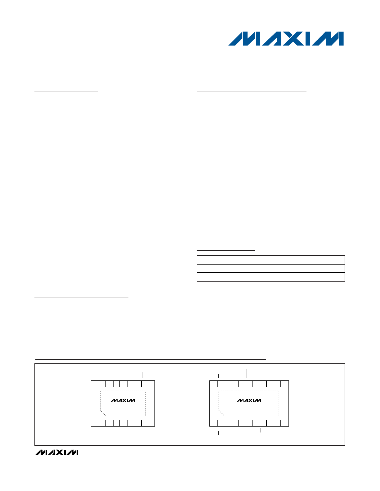
Pin Configurations
UL is a registered trademark of Underwriters Laboratories, Inc.
TEMP RANGE
-40°C to +85°C
-40°C to +85°C
OUT
8 7 6 5
MAX16023
+
1 2 3 4
CC
V
BATT
TDFN
*EP *EP
PFI
MR
*EP = EXPOSED PAD
OUT
MAX16024
CC
V
TDFN
RESET
BATT
CEOUT
10 9 8 7
+
1 2 3 4
CEIN
PFO
GND
RESET
GND
BATT ONSET
6
5
MR
Page 2
MAX16023/MAX16024
Battery-Backup Circuits with
Regulated Output Voltage
2 _______________________________________________________________________________________
ABSOLUTE MAXIMUM RATINGS
ELECTRICAL CHARACTERISTICS
(VCC= 1.53V to 5.5V, V
BATT
= 3V, reset not asserted, TA= TJ= -40°C to +85°C, C
OUT
= 10µF, unless otherwise noted. Typical val-
ues are at T
A
= TJ= +25°C.) (Note 2)
Stresses beyond those listed under “Absolute Maximum Ratings” may cause permanent damage to the device. These are stress ratings only, and functional
operation of the device at these or any other conditions beyond those indicated in the operational sections of the specifications is not implied. Exposure to
absolute maximum rating conditions for extended periods may affect device reliability.
VCC, BATT, OUT to GND..........................................-0.3V to +6V
RESET, PFO, BATT ON (all open drain)
to GND..................................................................-0.3V to +6V
RESET, PFO, BATT ON (all push-pull)
to GND .................................................-0.3V to (V
OUT
+ 0.3V)
PFI, CEIN, CEOUT to GND.......................-0.3V to (V
OUT
+ 0.3V)
MR to GND .................................................-0.3V to (V
CC
+ 0.3V)
Input Current
V
CC
Peak Current.....................................................................1A
V
CC
Continuous Current ...............................................250mA
BATT Peak Current .......................................................500mA
BATT Continuous Current ...............................................70mA
Output Current
OUT Short Circuit to GND Duration ....................................10s
RESET, BATT ON, CEOUT..............................................20mA
Continuous Power Dissipation (T
A
= +70°C)
8-Pin TDFN (derate 24.4mW/°C above +70°C) .........1951mW
10-Pin TDFN (derate 24.4mW/°C above +70°C) .......1951mW
Thermal Resistance (Note 1)
θ
JA
(8-Pin and 10-Pin TDFN)........................................41°C/W
Operating Temperature Range ...........................-40°C to +85°C
Junction Temperature......................................................+150°C
Storage Temperature Range .............................-65°C to +150°C
Lead Temperature (soldering, 10s) .................................+300°C
,
Note 1: Package thermal resistances were obtained using the method described in JEDEC specification JESD51-7, using a four-
layer board. For detailed information on package thermal considerations, refer to www.maxim-ic.com/thermal-tutorial
.
Operating Voltage Range V
Supply Current I
Supply Current in Battery-Backup
Mode
BATT Standby Current VCC > V
SET Reference Voltage V
SET Input Leakage Current MAX16024_TB_, SET = 1.2V -20 +20 nA
Output Voltage Range V
Output Voltage Accuracy I
PARAMETER SYMBOL CONDITIONS MIN TYP MAX UNITS
V
CC
BATT
CC
I
BATT
SET
OUT
(Note 3) 1.53 5.5 V
VCC = LDO + 0.5V,
no load
VCC = LDO + 0.5V,
I
= 20mA
OUT
VCC = 0, V
no dropout, no load
BATT
MAX16024_TB_, VCC = 2.2V 1.144 1.2 1.272 V
MAX16024_TB_, VCC > V
= 1mA
OUT
LDO = 1.2V 4.3 6
LDO = 1.8V 4.7 7
LDO = 2.5V 5.2 7.5
LDO = 3V 5.5 8
LDO = 3.3V 5.7 8
LDO = 1.2V 16 20
LDO = 1.8V 16 21
LDO = 2.5V 16 18.1
LDO = 3V 17 18.6
LDO = 3.3V 17 19
= 3V,
BATT
+ 0.2V -0.01 +0.01 µA
OUT
LDO = 1.2V 1.145 1.2 1.270
LDO = 1.8V 1.704 1.8 1.900
LDO = 2.5V 2.368 2.5 2.634
LDO = 3V 2.837 3 3.165
LDO = 3.3V 3.114 3.3 3.482
3.5 5.26 µA
1.8 5.25 V
µA
V
Page 3
MAX16023/MAX16024
Battery-Backup Circuits with
Regulated Output Voltage
_______________________________________________________________________________________ 3
ELECTRICAL CHARACTERISTICS (continued)
(VCC= 1.53V to 5.5V, V
BATT
= 3V, reset not asserted, TA= TJ= -40°C to +85°C, C
OUT
= 10µF, unless otherwise noted. Typical val-
ues are at T
A
= TJ= +25°C.) (Note 2)
PARAMETER SYMBOL CONDITIONS MIN TYP MAX UNITS
Line Regulation
Load Regulation VCC = V
Dropout Voltage
Output Current Limit
Battery Freshness Leakage
Current
RESET OUTPUT (RESET)
Reset Threshold V
VCC Falling to Reset Delay t
Reset Timeout Period t
RESET Output High Voltage
(Push-Pull Output)
RESET Output Leakage Current
(Open-Drain Output)
POWER-FAIL COMPARATOR (PFI, PFO)
PFI Input Threshold V
PFI Input Hysteresis V
PFI Input Current I
PFO Output Low Voltage
PFO Output High Voltage
(Push-Pull Output)
PFO Leakage Current
(Open-Drain Output)
PFO Delay Time (V
MANUAL RESET (MR)
Input Low Voltage V
Input High Voltage V
Pullup Resistance Pullup resistance to V
Glitch Immunity 100 ns
MR to Reset Delay 120 ns
V
I
OUT
I
OUT
CC
= (V
= 1mA
= 50mA
OUT
OUT
+ 1V, I
+ 1V) to (V
OUT
(Note 4)
VCC = 1.6V 75
V
≥ 2V 150
CC
= 5.5V 10 nA
V
BATT
TH
VCC falling at 10V/ms 20 µs
RD
VCC rising 145 215 285 ms
RP
V
OL
V
OH
PFT
PFI-HYS
PFI
IL
IH
= 3.3V, I
OUT
V
= 1.8V, I
OUT
V
= 1.2V, I
OUT
VCC ≥ 1.1 x VTH, I
RESET deasserted
= 5.5V, reset deasserted 1 µA
V
RESET
V
falling, 1.6V ≤ VCC ≤ 5.5V 0.570 0.590 0.611 V
PFI
V
= 1.8V, I
OUT
=1.2V, I
V
OUT
I
V
= 100µA, PFO deasserted V
SOURCE
= 5.5V, PFO deasserted 1 µA
PFO
+ 100mV) to (V
PFI
= 3.2mA, RESET asserted 0.3
SINK
= 1mA, RESET asserted 0.3RESET Output Low Voltage V
SINK
= 100µA, RESET asserted 0.3
SINK
SOURCE
= 1mA, PFO asserted 0.3
SINK
= 100µA, PFO asserted 0.3
SINK
PFI
CC
+ 2V),
OUT
0.2 1.0 %/V
= 1mA to 2mA 0.15 1.0 %
LDO = 1.2V 500
LDO = 1.8V 200
LDO = 2.5V 180
LDO = 3V 150
LDO = 3.3V 150
(See Table 1) V
= 100µA,
V
- 0.3V V
OUT
30 mV
-1 +1 µA
- 0.3V V
OUT
- 100mV) 20 µs
0.3 x V
CC
0.7 x V
CC
20 30 kΩ
mV
mA
V
V
V
Page 4
MAX16023/MAX16024
Battery-Backup Circuits with
Regulated Output Voltage
4 _______________________________________________________________________________________
ELECTRICAL CHARACTERISTICS (continued)
(VCC= 1.53V to 5.5V, V
BATT
= 3V, reset not asserted, TA= TJ= -40°C to +85°C, C
OUT
= 10µF, unless otherwise noted. Typical val-
ues are at T
A
= TJ= +25°C.) (Note 2)
Note 2: All devices are 100% production tested at TA= +25°C and TA= +85°C. Limits over temperature are guaranteed by design.
Note 3: V
BATT
can be 0 anytime or VCCcan go down to 0 if V
BATT
is active (except at startup).
Note 4: Dropout voltage is defined as (V
IN
- V
OUT
) when V
OUT
is 2% below the value of V
OUT
when VIN= V
OUT
+ 1V.
Note 5: CEIN to CEOUT resistance is tested with VCC= 5V and V
CEIN
= 0 or 5V.
Note 6: Use external current-limiting resistor to limit current to 20mA (max).
BATTERY-ON INDICATOR (BATT ON)
Output Low Voltage V
Output High Voltage
(Push-Pull Output)
Output Leakage Current
(Open-Drain Output)
Output Short-Circuit Current
CE GATING (CEIN, CEOUT)
CEIN Leakage Current Reset asserted, VCC = 0.9 x VTH or 0 -1 +1 µA
CEIN to CEOUT Resistance VCC = 5V, reset deasserted 8 50 Ω
CEOUT Short-Circuit Current Reset asserted, CEOUT = 0 0.75 2 mA
CEIN to CEOUT Propagation
Delay
Output High Voltage V
Reset to CEOUT Delay 12 µs
PARAMETER SYMBOL CONDITIONS MIN TYP MAX UNITS
V
= 1.2V, I
OUT
deasserted
V
= 1.8V, I
OL
V
OH
OH
OUT
deasserted
V
= 3.3V, I
OUT
deasserted
I
V
Sink current, V
(Note 6)
50Ω source, C
I
= 100µA, BATT ON asserted V
SOURCE
= 5.5V 1 µA
CC
= 100µA, reset asserted V
SOURCE
= 100µA, BATT ON
SINK
= 1mA, BATT ON
SINK
= 3.2mA, BATT ON
SINK
= 5V
CC
= 50pF, VCC = 4.75V 1.5 7 ns
LOAD
- 0.3V V
OUT
60 mA
- 0.3V V
OUT
0.3
0.3
0.3
V
Page 5
MAX16023/MAX16024
Battery-Backup Circuits with
Regulated Output Voltage
_______________________________________________________________________________________ 5
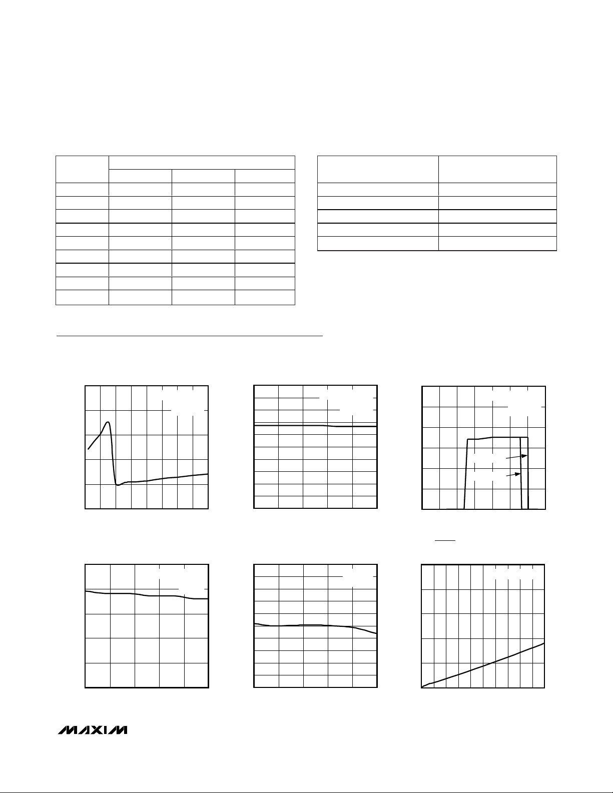
Typical Operating Characteristics
(V
CC
= 5V, V
BATT
= 0, I
OUT
= 0, TA= +25°C, unless otherwise noted.)
Table 1. Reset Threshold Ranges Table 2. Fixed Output Voltage
SUFFIX
RESET THRESHOLD RANGES (V)
MIN TYP MAX
L 4.508 4.63 4.906
M 4.264 4.38 4.635
T 2.991 3.08 3.239
S 2.845 2.93 3.080
R 2.549 2.63 2.755
Z 2.243 2.32 2.425
Y 2.117 2.19 2.288
W 1.603 1.67 1.733
V 1.514 1.575 1.639
SUFFIX
33 3.3
30 3.0
25 2.5
18 1.8
12 1.2
NOMINAL OUTPUT
VOLTAGE (V)
25
20
15
10
SUPPLY CURRENT (μA)
CC
V
5
0
1.5 5.5
VCC SUPPLY CURRENT
SUPPLY VOLTAGE
vs. V
CC
MAX16024PTBS25+
3.02.5 4.52.0 3.5 5.04.0
VCC SUPPLY VOLTAGE (V)
VCC SUPPLY CURRENT
vs. TEMPERATURE
10
V
V
OUT
= 2.93V
TH
= 2.5V
MAX16023 toc01
9
8
7
6
5
4
SUPPLY CURRENT (μA)
3
CC
V
2
1
0
-40 85
TEMPERATURE (°C)
MAX16024PTBS25+
V
V
OUT
= 2.93V
TH
6010 35-15
= 2.5V
MAX16023 toc02
BATT SUPPLY CURRENT
SUPPLY VOLTAGE
vs. V
6
5
4
3
2
BATT SUPPLY CURRENT (μA)
1
0
0 3.5
CC
V
V
1.0 3.00.5 2.52.01.5
VCC SUPPLY VOLTAGE (V)
MAX16024PTBS25+
= 3.0V
BATT
= 2.8V
BATT
V
V
OUT
= 2.93V
TH
= 2.5V
MAX16023 toc03
BATTERY SUPPLY CURRENT
vs. TEMPERATURE
5
4
3
2
1
BATTERY SUPPLY CURRENT (μA)
0
-40 85
TEMPERATURE (°C)
MAX16024PTBS25+
V
BATT
= +3.0V
V
CC
6010 35-15
= 0
10
8
MAX16023 toc04
6
4
2
0
-2
-4
BATT STANDBY CURRENT (nA)
-6
-8
-10
-40 85
BATT STANDBY CURRENT
vs. TEMPERATURE
VCC = 3.3V
V
BATT
TEMPERATURE (°C)
= 3.0V
6010 35-15
1.0
MAX16023 toc05
0.8
0.6
0.4
OUTPUT VOLTAGE LOW (V)
0.2
0
02014610218
RESET OUTPUT VOLTAGE LOW
vs. SINK CURRENT
MAX16024PTBS25+
MAX16023 toc06
168124
SINK CURRENT (mA)
Page 6
MAX16023/MAX16024
Battery-Backup Circuits with
Regulated Output Voltage
6 _______________________________________________________________________________________
Typical Operating Characteristics (continued)
(V
CC
= 5V, V
BATT
= 0, I
OUT
= 0, TA= +25°C, unless otherwise noted.)
VCC FALLING TO RESET DELAY
vs. TEMPERATURE
MAX16023 toc07
TEMPERATURE (°C)
DELAY (μs)
6010 35-15
20
40
60
80
100
10
30
50
70
90
0
-40 85
VCC FALLING 10V/ms
RESET TIMEOUT PERIOD
vs. TEMPERATURE
MAX16023 toc08
TEMPERATURE (°C)
RESET TIMEOUT PERIOD (ms)
6035-15 10
185
190
195
200
210
205
215
220
180
-40 85
NORMALIZED RESET THRESHOLD
vs. TEMPERATURE
MAX16023 toc09
TEMPERATURE (°C)
NORMALIZED RESET THRESHOLD
6010 35-15
0.990
1.005
1.015
1.020
0.985
0.995
1.000
1.010
0.980
-40 85
MAX16024PTBS25+
V
OUT
= 2.5V
MAXIMUM TRANSIENT DURATION
vs. RESET THRESHOLD OVERDRIVE
RESET THRESHOLD OVERDRIVE (mV)
TRANSIENT DURATION (ms)
MAX16023 toc10
0 200 400 600 800 1000
0
25
50
75
100
125
150
175
200
RESET OCCURS ABOVE THE CURVE
DROPOUT VOLTAGE
vs. LOAD CURRENT
MAX16023 toc11
LOAD CURRENT (mA)
DROPOUT VOLTAGE (mV)
8040 6020
150
350
450
500
100
300
50
200
250
400
0
01007030 5010 90
MAX16024PTBS25+
OUTPUT VOLTAGE
vs. LOAD CURRENT
MAX16023 toc12
LOAD CURRENT (mA)
OUTPUT VOLTAGE (V)
8040 6020
2.42
2.58
2.66
2.70
2.38
2.54
2.34
2.46
2.50
2.62
2.30
01007030 5010 90
MAX16024PTBS25+
V
OUT
= 2.5V
TA = -40°C
TA = +25°C
TA = +85°C
Page 7

OUTPUT VOLTAGE
vs. V
CC
VOLTAGE
MAX16023 toc13
VCC VOLTAGE (V)
OUTPUT VOLTAGE (V)
14
2.1
2.5
2.7
2.8
2.0
2.4
1.9
1.8
1.7
1.6
2.2
2.3
2.6
1.5
0623 5
MAX16024PTBS25+
I
OUT
= 0
LOAD-TRANSIENT RESPONSE
MAX16023 toc14
1ms/div
OUT
AC-COUPLED
100mV/div
50mA
I
OUT
20mA/div
10mA
MAX16024PTBS25+
C
OUT
= 10μF
STARTUP RESPONSE
MAX16023 toc15
2ms/div
V
CC
2V/div
OUT
1V/div
MAX16024PTBS25+
I
OUT
= 0
MAX16023/MAX16024
Battery-Backup Circuits with
Regulated Output Voltage
_______________________________________________________________________________________ 7
Typical Operating Characteristics (continued)
(V
CC
= 5V, V
BATT
= 0, I
OUT
= 0, TA= +25°C, unless otherwise noted.)
MR FALLING TO RESET DELAY
MAX16023 toc16
CHIP-ENABLE LOCKING OUT
SIGNAL DURING RESET
MAX16023 toc17
MR
5V/div
RESET
5V/div
200ns/div
40μs/div
RESET
5V/div
CEIN
2V/div
CEOUT
2V/div
Page 8

MAX16023/MAX16024
Battery-Backup Circuits with
Regulated Output Voltage
8 _______________________________________________________________________________________
Pin Description
PIN
MAX16023 MAX16024
12VCCSupply Voltage Input. Bypass V
2 3 BATT
34MR
4 — PFI
5—PFO
6 7 GND Ground
78RESET
8 9 OUT
—1CEIN
— 5 SET
— 6 BATT ON
—10CEOUT
——EP
NAME FUNCTION
Backup Battery Input. If V
the regulator enters dropout, the regulator is powered from BATT. If V
the regulator is powered from V
Active-Low, Manual-Reset Input. RESET asserts when MR is pulled low. RESET
remains low for the duration of reset timeout period after MR transitions from low to
high. Connect MR to OUT or leave unconnected if not used. MR is internally
connected to V
Power-Fail Comparator Input. Connect PFI to a resistive divider to set the desired PFI
threshold. The PFI input is referenced to an internal V
internal hysteresis provides noise immunity. The power-fail comparator is powered
from OUT.
Active-Low, Power-Fail Comparator Output. PFO goes low when V
internal V
hysteresis.
Active-Low Reset Output. RESET asserts when V
MR is pulled low. RESET remains low for the duration of the reset timeout period after
V
CC
pull and open-drain options.
Linear Regulator Output Voltage. Available in the following factory-fixed voltages of
1.2V, 1.8V, 2.5V, 3.0V, or 3.3V for all devices. The MAX16024 is also available with
an adjustable output voltage (1.8V to 5.25V). Bypass OUT to GND with a 10µF
capacitor.
Chip-Enable Input. The input to CE gating circuitry. Connect to GND or OUT if not
used.
Set Output Voltage Input. For the fixed output voltage versions (MAX16024_TB_),
SET is not used. Connect SET to GND. For MAX16024_TB_, connect SET to an
external resistive divider to set the desired output voltage between 1.8V and 5.25V.
Active-High, Battery-On Output. BATT ON goes high when in the battery backup
mode.
Active-Low, Chip-Enable Output. CEOUT goes low only when CEIN is low and reset
is not asserted. If CEIN is low when reset is asserted, CEOUT stays low for 12µs (typ)
or until CEIN goes high, whichever occurs first.
Exposed Pad. Internally connected to GND. Connect EP to a large ground plane to
aid heat dissipation. Do not use EP as the only ground connection for the device.
PFT
rises above the reset threshold and MR goes high. RESET is available in push-
through a 30kΩ pullup resistor.
CC
threshold and goes high when V
to GND with a 0.1µF capacitor.
CC
falls below its reset threshold (VTH), V
CC
. Bypass BATT to GND with a 0.1µF capacitor.
CC
threshold. A V
PFT
rises above V
PFI
falls below the reset threshold or
CC
BATT
BATT
falls below the
PFI
+ V
PFT
≥ VCC, and if
< VCC,
PFT-HYS
PFT-HYS
Page 9

MAX16023/MAX16024
Battery-Backup Circuits with
Regulated Output Voltage
_______________________________________________________________________________________ 9
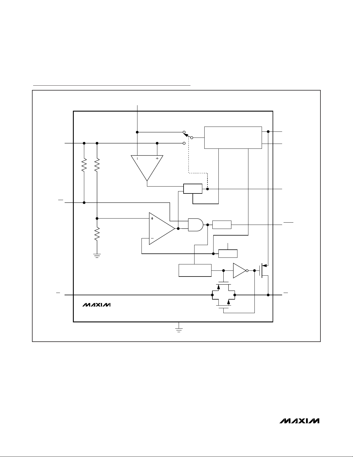
Functional Diagrams
BATT
V
CC
LOGIC
MR
DROPOUT
RESET DELAY
LDO
OUT
OUT
RESET
PFI
REF
OUT
PFO
MAX16023
GND
Page 10
MAX16023/MAX16024
Battery-Backup Circuits with
Regulated Output Voltage
10 ______________________________________________________________________________________
Functional Diagrams (continued)
BATT
V
CC
OUT
LDO
SET
MR
CEIN
MAX16024
LOGIC
DROPOUT
RESET DELAY
CE OUTPUT
CONTROL
GND
V
REF
BATT ON
RESET
CC
CEOUT
Page 11

Detailed Description
The
Typical Applications Circuit
shows a typical connection using the MAX16024. OUT powers the SRAM. If
VCCis higher than the reset threshold (VTH), or if V
CC
is
lower than V
TH
but higher than V
BATT
, the regulator is
powered from VCC. If V
CC
< VTH, VCC< V
BATT
, and the
regulator is in dropout, the regulator is powered from
BATT (see the
Functional Diagrams
). OUT supplies up
to 100mA from VCC.
Backup-Battery Switchover
In a brownout or power failure, it may be necessary to
preserve the contents of the RAM. With a backup-battery installed at BATT, the MAX16023/MAX16024 automatically switch the RAM to backup power when V
CC
falls. The MAX16024 has a BATT ON output that goes
high when in battery-backup mode. Three conditions
must be met for these devices to switch to battery
backup mode:
1) VCCis lower than the reset threshold.
2) VCCis lower than V
BATT
.
3) The regulator is in dropout (except for the 1.2V out-
put version).
Chip-Enable Signal Gating (MAX16024)
The MAX16024 provides internal gating of CE signals to
prevent erroneous data from being written to CMOS
RAM in the event of a power failure or brownout. During
normal operation, the CE gate enables and passes all
CE transitions. When the reset output asserts, this path
becomes disabled, preventing erroneous data from corrupting the CMOS RAM and CEOUT is pulled up to OUT
through an internal current source. The 1.5ns propagation delay from CEIN to CEOUT allows the devices to
be used with most µPs and high-speed DSPs.
During normal operation (reset not asserted), CEIN is
connected to CEOUT through a low on-resistance
transmission gate. If CEIN is high when a reset asserts,
CEOUT remains high regardless of any subsequent
transition on CEIN during the reset event.
If CEIN is low when reset asserts, CEOUT is held low for
12µs to allow completion of the read/write operation.
After the 12µs delay expires, CEOUT goes high and
stays high regardless of any subsequent transitions on
CEIN during the reset event. When CEOUT is disconnected from CEIN, CEOUT is actively pulled up to OUT.
The propagation delay through the chip-enable circuitry
depends on both the source impedance of the drive to
CEIN and the capacitive loading at CEOUT. Minimize
the capacitive load at CEOUT to minimize propagation
delay, and use a low-output-impedance driver.
MAX16023/MAX16024
Battery-Backup Circuits with
Regulated Output Voltage
______________________________________________________________________________________ 11
Figure 1. Reset and Chip-Enable Timing
V
RESET THRESHOLD V
CC
TH
CEIN
CEOUT
RESET-TO-CEOUT DELAY (12μs)
RESET
*
t
RD
t
RD
t
RP
*
IF CEIN GOES HIGH BEFORE RESET ASSERTS,
CEOUT GOES HIGH WITHOUT DELAY AS
CEIN GOES HIGH.
t
RP
Page 12

MAX16023/MAX16024
Manual-Reset Input
(MAX16023/MAX16024)
Many µP-based products require manual-reset capability, allowing the operator, a test technician, or external
logic circuitry to initiate a reset. For the MAX16023/
MAX16024, a logic-low on MR asserts RESET. RESET
remains asserted while MR is low. When MR goes high,
RESET deasserts after a minimum of 145ms (tRP). MR
has an internal 30kΩ pullup resistor to VCC. MR can be
driven with TTL/CMOS logic levels or with opendrain/collector outputs. Connect a normally open
momentary switch from MR to GND to create a manualreset function; external debounce circuitry is not
required. If MR is driven from a long cable or the device
is used in a noisy environment, connect a 0.1µF capacitor from MR to GND to provide additional noise immunity.
Battery-On Indicator (MAX16024)
The MAX16024’s BATT ON output goes high when in
battery-backup mode. Use BATT ON to indicate battery-switchover status.
Battery Freshness Seal
The MAX16023/MAX16024 battery freshness seal disconnects the backup battery from internal circuitry and
OUT until VCCis applied. This ensures the backup battery connected to BATT is fresh when the final product
is used for the first time.
The internal freshness seal latch prevents BATT from
powering OUT until VCChas come up for the first time,
setting the latch. When VCCsubsequently turns off,
BATT begins to power OUT.
To reenable the freshness seal (MAX16023/
MAX16024):
1) Connect a battery to BATT.
2) Bring VCCto 0.
3) Drive MR higher than V
BATT
+ 1.2V for at least 3µs.
4) Pull OUT to 0.
Reset Output (MAX16023/MAX16024)
A µP’s reset input starts the µP in a known state. The
MAX16023/MAX16024 µP supervisory circuits assert a
reset to prevent code-execution errors during powerup, power-down, and brownout conditions. RESET
asserts when VCCis below the reset threshold and
remains low for at least 145ms (tRP) after VCCrises
above the reset threshold. RESET also asserts when
MR is low. RESET is available in both push-pull and
open-drain configurations.
Power-Fail Comparator (MAX16023)
The MAX16023 offers an additional undervoltage comparator. The output PFO goes low when the voltage at
PFI falls below its V
PFT
threshold. Common uses for the
power-fail comparator include monitoring the input of the
power supply (such as a battery) before any voltage regulation to provide an early power-fail warning, so software can conduct an orderly system shutdown. The
power-fail comparator has a typical input hysteresis of
V
PFT-HYS
and is powered from OUT, making it indepen-
dent of the reset circuit. Connect PFI to GND, if not used.
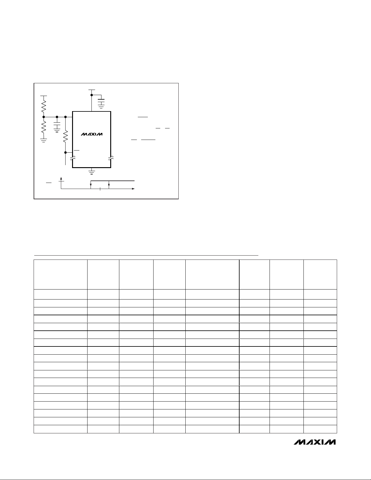
Regulator Output
Fixed output voltages of 1.2V, 1.8V, 2.5V, 3.0V, and
3.3V are available for all devices. The regulator output
delivers up to 100mA of load current.
The MAX16024 is available with both fixed and
adjustable output-voltage options. Use an external
resistive divider network connected between OUT, SET,
and GND (Figure 2) to set the adjustable output voltage
from 1.8V to 5.25V. Connect SET to GND for parts with
fixed output voltage option.
Battery-Backup Circuits with
Regulated Output Voltage
12 ______________________________________________________________________________________
Figure 2. Setting the Adjustable Output Voltage (MAX16024
Only)
1.53 TO 5.5V
0.1μF
V
CC
MAX16024
RESETTO μP
GND
OUT
SET
1.8V TO 5.25V
10μF
R1
R2
= V
OUT
SET
= 1.2V
(1 + R1/R2)
SET
V
V
Page 13

Applications Information
The MAX16023/MAX16024 are protected for typical
short-circuit conditions of 10s or less. Shorting OUT to
ground for longer than 10s might damage the device.
Bypass VCCand BATT to GND with a 0.1µF capacitor
each. Connect a 10µF low-ESR capacitor from OUT to
GND. All capacitors should be mounted as close as
possible to the device.
Monitoring an Additional Supply
The MAX16023 power-fail comparator can monitor
either positive or negative supplies using a resistive
divider to PFI (Figures 3 and 4). PFO can be used to
generate an interrupt to the µP or to trigger a reset. To
monitor a negative supply, connect the top of the resistive divider to VCC. Connect the bottom of the resistive
divider to the negative voltage to be monitored.
Adding Hysteresis to PFI
The power-fail comparators have a typical input hysteresis of V
PFT-HYS
. This is sufficient for most applications where a power-supply line is being monitored
through an external voltage-divider (see the
Monitoring
an Additional Supply
section). Figure 5 shows how to
add hysteresis to the power-fail comparator. Select the
ratio of R1 and R2 such that PFI sees V
PFT
when V
IN
falls to the desired trip point (V
TRIP
). Resistor R3 adds
hysteresis. R3 is typically an order of magnitude greater
than R1 or R2. The current through R1 and R2 should
be at least 100µA to ensure that the 1µA (max) PFI
input current does not shift the trip point. R3 should be
larger than 50kΩ to prevent it from loading down PFO.
Capacitor C1 adds additional noise rejection.
MAX16023/MAX16024
Battery-Backup Circuits with
Regulated Output Voltage
______________________________________________________________________________________ 13
Figure 3. Monitoring an Additional Supply by Connecting PFO
to MR
Figure 4. Monitoring a Negative Supply
V
1
0.1μF
V
2
V
CC
R1
PFI
MAX16023L
R2
RESET
PFO
MR
RESET
μP
5V
R1
R2
V-
0.1μF
V
CC
PFI
MAX16023
PFO
GND
ADDITIONAL SUPPLY RESET VOLTAGE
= V
PFT
R1 + R2
x
( )
R2
V
2(RESET)
GND
+5V
PFO
0
V
TRIP
V
V
0
= V
TRIP
IS NEGATIVE
TRIP
R2
- (5 - V
PFT
R2
V-
PFT
)
Page 14
MAX16023/MAX16024
Operation Without a Backup
Power Source
The MAX16023/MAX16024 provide battery-backup
functions. If a backup power source is not used, connect BATT to GND.
Replacing the Backup Battery
When VCCis above VTH, the backup power source can
be removed without danger of triggering a reset pulse.
The device does not enter battery-backup mode when
V
CC
stays above the reset threshold voltage.
Negative-Going VCCTransients
The MAX16023/MAX16024 are relatively immune to
short duration, negative-going VCCtransients.
Resetting the µP when VCCexperiences only small
glitches is usually not desirable. A 0.1µF bypass
capacitor mounted close to the VCCpin provides additional transient immunity.
Capacitor Selection and
Regulator Stability
For stable operation, connect a low-ESR 10µF (min) output capacitor from OUT to GND. To reduce noise and
improve load-transient response and power-supply rejection, use larger output capacitor values.
Battery-Backup Circuits with
Regulated Output Voltage
14 ______________________________________________________________________________________
Figure 5. Adding Hysteresis to the Power-Fail Comparator
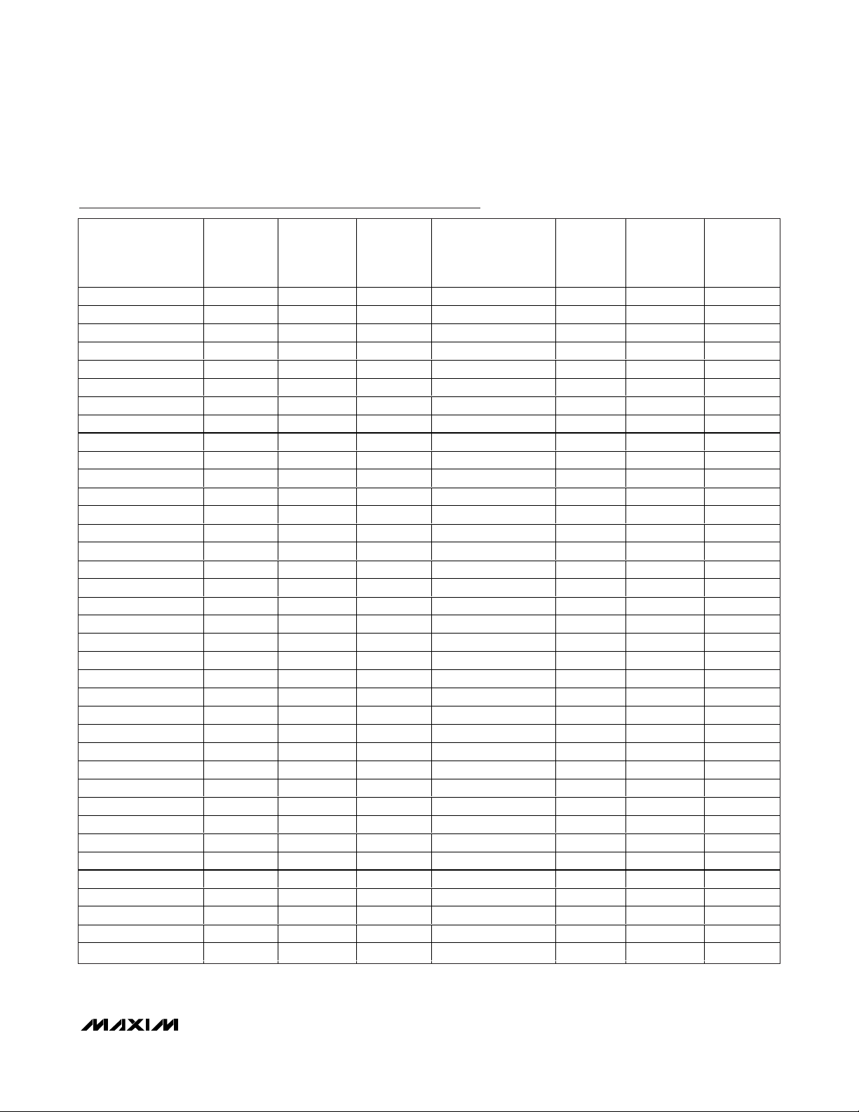
Part Number Table
+5V
V
IN
V
GND
V
0.1μF
CC
V
L
TRIP
V
V
TRIP
VH = (V
VL = R1 x
WHERE V
THRESHOLD VOLTAGE.
H
R1 + R2
= V
x
PFT
( )
+ V
PFT
PFT - HYS
V
PFT
( - )
R2
IS THE POWER-FAIL
PFT
V
IN
R2
)
VCC - V
R3
*OPTIONAL
R1R2R1
x ( +
PFT
+ V
R1
PFI
C1*
R2
PFO
R3
TO μP
+5V
0
MAX16023
PFO
PART
OUTPUT
TYPE
R ESET
T H R ESH O L D
VO L T A G E
( V)
REGUL ATED
VO LTA GE
+ 1
R3
PFT
OU TPU T
( V)
)
R ESET
PART
OUTPUT
TYPE
T H R ESH O L D
VO L T A G E
( V)
R EG U L A T ED
O U T PU T
VO L T A G E
( V)
MAX16023LTAL12+T Push-Pull 4.63 1.2 MAX16024LTBL12+T Push-Pull 4.63 1.2
MAX16023LTAL18+T Push-Pull 4.63 1.8 MAX16024LTBL18+T Push-Pull 4.63 1.8
MAX16023LTAL25+T Push-Pull 4.63 2.5 MAX16024LTBL25+T Push-Pull 4.63 2.5
MAX16023LTAL33+T Push-Pull 4.63 3.3 MAX16024LTBL33+T Push-Pull 4.63 3.3
MAX16023LTAM12+T Push-Pull 4.38 1.2 MAX16024LTBM12+T Push-Pull 4.38 1.2
MAX16023LTAM18+T Push-Pull 4.38 1.8 MAX16024LTBM18+T Push-Pull 4.38 1.8
MAX16023LTAM25+T Push-Pull 4.38 2.5 MAX16024LTBM25+T Push-Pull 4.38 2.5
MAX16023LTAM33+T Push-Pull 4.38 3.3 MAX16024LTBM33+T Push-Pull 4.38 3.3
MAX16023LTAT12+T Push-Pull 3.08 1.2 MAX16024LTBT12+T Push-Pull 3.08 1.2
MAX16023LTAT18+T Push-Pull 3.08 1.8 MAX16024LTBT18+T Push-Pull 3.08 1.8
MAX16023LTAT25+T Push-Pull 3.08 2.5 MAX16024LTBT25+T Push-Pull 3.08 2.5
MAX16023LTAS12+T Push-Pull 2.93 1.2 MAX16024LTBS12+T Push-Pull 2.93 1.2
MAX16023LTAS18+T Push-Pull 2.93 1.8 MAX16024LTBS18+T Push-Pull 2.93 1.8
MAX16023LTAS25+T Push-Pull 2.93 2.5 MAX16024LTBS25+T Push-Pull 2.93 2.5
MAX16023LTAR12+T Push-Pull 2.63 1.2 MAX16024LTBR12+T Push-Pull 2.63 1.2
MAX16023LTAR18+T Push-Pull 2.63 1.8 MAX16024LTBR18+T Push-Pull 2.63 1.8
MAX16023LTAR25+T Push-Pull 2.63 2.5 MAX16024LTBR25+T Push-Pull 2.63 2.5
MAX16023LTAZ12+T Push-Pull 2.32 1.2 MAX16024LTBZ12+T Push-Pull 2.32 1.2
Page 15
MAX16023/MAX16024
Battery-Backup Circuits with
Regulated Output Voltage
______________________________________________________________________________________ 15
Part Number Table (continued)
Bold parts denote standard versions. Samples are generally available on standard versions.
Contact factory for availability of nonstandard versions.
R ESET
PART
MAX16023LTAZ18+T Push-Pull 2.32 1.8 MAX16024LTBZ18+T Push-Pull 2.32 1.8
MAX16023LTAY12+T Push-Pull 2.19 1.2 MAX16024LTBY12+T Push-Pull 2.19 1.2
MAX16023LTAY18+T Push-Pull 2.19 1.8 MAX16024LTBY18+T Push-Pull 2.19 1.8
MAX16023LTAW12+T Push-Pull 1.67 1.2 MAX16024LTBW12+T Push-Pull 1.67 1.2
MAX16023LTAV12+T Push-Pull 1.575 1.2 MAX16024LTBV12+T Push-Pull 1.575 1.2
MAX16023PTAL12+T Open-Drain 4.63 1.2 MAX16024PTBL12+T Open-Drain 4.63 1.2
MAX16023PTAL18+T Open-Drain 4.63 1.8 MAX16024PTBL18+T Open-Drain 4.63 1.8
MAX16023PTAL25+T Open-Drain 4.63 2.5 MAX16024PTBL25+T Open-Drain 4.63 2.5
MAX16023PTAL33+T Open-Drain 4.63 3.3 MAX16024PTBL33+T Open-Drain 4.63 3.3
MAX16023PTAM12+T Open-Drain 4.38 1.2 MAX16024PTBM12+T Open-Drain 4.38 1.2
MAX16023PTAM18+T Open-Drain 4.38 1.8 MAX16024PTBM18+T Open-Drain 4.38 1.8
MAX16023PTAM25+T Open-Drain 4.38 2.5 MAX16024PTBM25+T Open-Drain 4.38 2.5
MAX16023PTAM33+T Open-Drain 4.38 3.3 MAX16024PTBM33+T Open-Drain 4.38 3.3
MAX16023PTAT12+T Open-Drain 3.08 1.2 MAX16024PTBS12+T Open-Drain 3.08 1.2
MAX16023PTAT18+T Open-Drain 3.08 1.8 MAX16024PTBS18+T Open-Drain 3.08 1.8
MAX16023PTAT25+T Open-Drain 3.08 2.5 MAX16024PTBS25+T O p e n - D r a i n 3.08 2.5
MAX16023PTAS12+T Open-Drain 2.93 1.2 MAX16024PTBT12+T Open-Drain 2.93 1.2
MAX16023PTAS18+T Open-Drain 2.93 1.8 MAX16024PTBT18+T Open-Drain 2.93 1.8
MAX16023PTAS25+T Open-Drain 2.93 2.5 MAX16024PTBT25+T Open-Drain 2.93 2.5
MAX16023PTAR12+T Open-Drain 2.63 1.2 MAX16024PTBR12+T Open-Drain 2.63 1.2
MAX16023PTAR18+T Open-Drain 2.63 1.8 MAX16024PTBR18+T Open-Drain 2.63 1.8
MAX16023PTAR25+T Open-Drain 2.63 2.5 MAX16024PTBR25+T Open-Drain 2.63 2.5
MAX16023PTAZ12+T Open-Drain 2.32 1.2 MAX16024PTBZ12+T Open-Drain 2.32 1.2
MAX16023PTAZ18+T Open-Drain 2.32 1.8 MAX16024PTBZ18+T Open-Drain 2.32 1.8
MAX16023PTAY12+T Open-Drain 2.19 1.2 MAX16024PTBY12+T Open-Drain 2.19 1.2
MAX16023PTAY18+T Open-Drain 2.19 1.8 MAX16024PTBY18+T Open-Drain 2.19 1.8
MAX16023PTAW12+T Open-Drain 1.67 1.2 MAX16024PTBW12+T Open-Drain 1.67 1.2
MAX16023PTAV12+T Open-Drain 1.575 1.2 MAX16024PTBV12+T Open-Drain 1.575 1.2
MAX16024PTBL+T Open-Drain 4.63 Adjustable MAX16024LTBL+T Push-Pull 4.63 Adjustable
MAX16024PTBM+T Open-Drain 4.38 Adjustable MAX16024LTBM+T Push-Pull 4.38 Adjustable
MAX16024PTBT+T Open-Drain 3.08 Adjustable MAX16024LTBT+T Push-Pull 3.08 Adjustable
MAX16024PTBS+T Open-Drain 2.93 Adjustable MAX16024LTBS+T Push-Pull 2.93 Adjustable
MAX16024PTBR+T Open-Drain 2.63 Adjustable MAX16024LTBR+T Push-Pull 2.63 Adjustable
MAX16024PTBZ+T Open-Drain 2.32 Adjustable MAX16024LTBZ+T Push-Pull 2.32 Adjustable
MAX16024PTBY+T Open-Drain 2.19 Adjustable MAX16024LTBY+T Push-Pull 2.19 Adjustable
MAX16024PTBW+T Open-Drain 1.67 Adjustable MAX16024LTBW+T Push-Pull 1.67 Adjustable
MAX16024PTBV+T Open-Drain 1.575 Adjustable MAX16024LTBV+T Push-Pull 1.575 Adjustable
OUTPUT
TYPE
T H R ESH O L D
VO L T A G E
( V)
REGUL ATED
OU TPU T
VO LTA GE
( V)
PART
OUTPUT
TYPE
R ESET
T H R ESH O L D
VO L T A G E
( V)
R EG U L A T ED
O U T PU T
VO L T A G E
( V)
Page 16
MAX16023/MAX16024
Battery-Backup Circuits with
Regulated Output Voltage
16 ______________________________________________________________________________________
Typical Applications Circuit
Selector Guide
OUTPUTS
PART
MAX16023L Push-Pull √√ √ — — Fixed
MAX16023P Open Drain √√ √ — — Fixed
MAX16024L Push-Pull √√ — √√Fixed/adjustable
MAX16024P Open Drain √√ — √√Fixed/adjustable
(RESET, PFO,
BATT ON )
RESET MR
POWER-FAIL
COMPARATOR
CE
GATE
BATT ON
3.3V
REGULATOR
OUTPUT VOLTAGE
0.1μF
BATT
0.1μF
3V
MAX16024L
MR
PUSHBUTTON
SET
V
GND
0.1μF
V
CC
RESET
BATT ON
OUT
CEOUT
CEIN
10μF
ADDRESS
DECODE
RST
CC
μP
A0–A15
RAM
CE
RTC
Page 17

MAX16023/MAX16024
Battery-Backup Circuits with
Regulated Output Voltage
Maxim cannot assume responsibility for use of any circuitry other than circuitry entirely embodied in a Maxim product. No circuit patent licenses are
implied. Maxim reserves the right to change the circuitry and specifications without notice at any time.
Maxim Integrated Products, 120 San Gabriel Drive, Sunnyvale, CA 94086 408-737-7600 ____________________
17
© 2008 Maxim Integrated Products is a registered trademark of Maxim Integrated Products, Inc.
Package Information
For the latest package outline information and land patterns, go
to www.maxim-ic.com/packages
.
PACKAGE TYPE PACKAGE CODE DOCUMENT NO.
8 TDFN T833-2
21-0137
10 TDFN T1033-1
21-0137
Chip Information
PROCESS: BiCMOS
 Loading...