

Page 1
General Description
The MAX16016/MAX16020/MAX16021 supervisory circuits monitor power supplies, provide battery-backup
control, and chip-enable (CE) gating to write protect
memory in microprocessor (µP)-based systems. These
low-power devices improve system reliability by providing
several supervisory functions in a small, single integrated
solution.
The MAX16016/MAX16020/MAX16021 perform four
basic system functions:
1) Provide a µP reset output during V
CC
supply power-
up, power-down, and brownout conditions.
2) Control V
CC
to battery-backup switching internally
to maintain data or low-power operation for memories, real-time clocks (RTCs), and other digital logic
when the main power is removed.
3) Provide memory write protection through internal
chip-enable gating during brownout.
4) Provide a combination of additional supervisory
functions listed in the
Features
section.
The MAX16016/MAX16020/MAX16021 operate from a
1.53V to 5.5V supply voltage and offer fixed reset
thresholds for monitoring 5V, 3.3V, 3V, 2.5V, and 1.8V
systems. Each device is available with either a pushpull or open-drain reset output.
The MAX16016/MAX16020/MAX16021 are available in
small TDFN/TQFN packages and are fully specified for
an operating temperature range of -40°C to +85°C.
Applications
Main/Backup Power for RTCs, CMOS Memories
Industrial Control
GPS Systems
Set-Top Boxes
Point-of-Sale Equipment
Portable/Battery Equipment
Features
o System Monitoring for 5V, 3.3V, 3V, 2.5V, or 1.8V
Power-Supply Voltages
o 1.53V to 5.5V Operating Voltage Range
o Low 1.2µA Supply Current (0.25µA in Battery-
Backup Mode)
o 145ms (min) Reset Timeout Period
o Battery Freshness Seal
o On-Board Gating of CE Signals, 1.5ns
Propagation Delay (MAX16020/MAX16021)
o Debounced Manual Reset Input
o Watchdog Timer, 1.2s (typ) Timeout
o Power-Fail Comparator and Low-Line Indicator for
Monitoring Voltages Down to 0.6V
o Battery-On, Battery-OK, and Battery Test
Indicators
o Small 10-Pin TDFN or 16-Pin TQFN Packages
o UL
®
-Certified to Conform to IEC 60950-1
MAX16016/MAX16020/MAX16021
Low-Power µP Supervisory Circuits with
Battery-Backup Circuit and Chip-Enable Gating
________________________________________________________________
Maxim Integrated Products
1
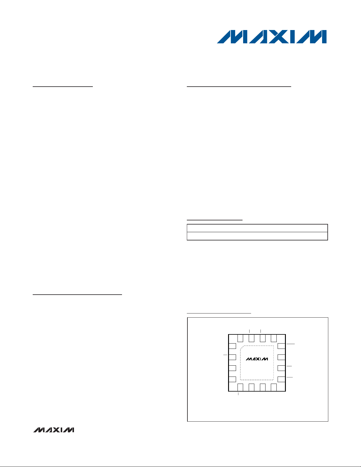
Pin Configurations
19-4145; Rev 3; 12/08
For pricing, delivery, and ordering information, please contact Maxim Direct at 1-888-629-4642,
or visit Maxim’s website at www.maxim-ic.com.
Ordering Information continued at end of data sheet.
Pin Configurations continued at end of data sheet.
Selector Guide located at end of data sheet.
Ordering Information
PART TEMP RANGE
PIN-PACKAGE
MAX16016_TB_+T -40°C to +85°C 10 TDFN-EP*
The first placeholder “_” designates all output options. Letter
“L” indicates push-pull outputs and letter “P” indicates opendrain outputs. The last placeholder “_” designates the reset
threshold (see Table 1).
T = Tape and reel.
+
Denotes a lead(Pb)-free/RoHS-compliant package.
*
EP = Exposed pad.
UL is a registered trademark of Underwriters Laboratories, Inc.
TOP VIEW
VCCCEIN
16
BATT
*EP = EXPOSED PAD.
+
MR
PFI
WDI
5156
LL
CEOUT
OUT
14713
RESET
121
GND
112
MAX16020
*EP
BATTOK
BATT_TEST
TQFN
8
BATTON
PFO
103
WDO
94
Page 2
MAX16016/MAX16020/MAX16021
Low-Power µP Supervisory Circuits with
Battery-Backup Circuit and Chip-Enable Gating
2 _______________________________________________________________________________________
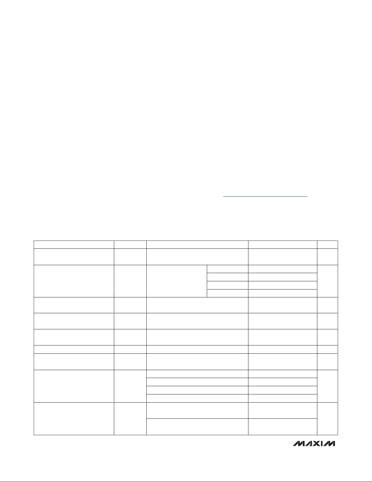
ABSOLUTE MAXIMUM RATINGS
ELECTRICAL CHARACTERISTICS
(VCC= 1.53V to 5.5V, V
BATT
= 3V, TA= -40°C to +85°C, unless otherwise noted. Typical values are at TA= +25°C.) (Note 2)
Stresses beyond those listed under “Absolute Maximum Ratings” may cause permanent damage to the device. These are stress ratings only, and functional
operation of the device at these or any other conditions beyond those indicated in the operational sections of the specifications is not implied. Exposure to
absolute maximum rating conditions for extended periods may affect device reliability.
VCC, BATT, OUT, BATT_TEST to GND.....................-0.3V to +6V
RESET, RESET, PFO, BATTOK, WDO, BATTON,
BATT_TEST, LL, (all open-drain) to GND .....................-0.3V to +6V
RESET, RESET, BATTOK, WDO, BATTON,
LL (all push-pull) to GND......................-0.3V to (V
OUT
+ 0.3V)
WDI, PFI to GND.......................................-0.3V to (V
OUT
+ 0.3V)
CEIN, CEOUT to GND ..............................-0.3V to (V
OUT
+ 0.3V)
MR to GND .................................................-0.3V to (V
CC
+ 0.3V)
Input Current
V
CC
Peak Current.................................................................1A
V
CC
Continuous Current ...............................................250mA
BATT Peak Current .......................................................500mA
BATT Continuous Current ...............................................70mA
Output Current
OUT Short Circuit to GND Duration ....................................10s
RESET, RESET, BATTON ....................................................20mA
Continuous Power Dissipation (T
A
= +70°C)
10-Pin TDFN (derate 24.4mW/°C above +70°C) .......1951mW
16-Pin TQFN (derate 25mW/°C above +70°C) ..........2000mW
Thermal Resistance (Note 1)
For 10-Pin TDFN
θ
JA
................................................................................41°C/W
For 16-Pin TQFN
θ
JA
................................................................................40°C/W
Operating Temperature Range ...........................-40°C to +85°C
Junction Temperature......................................................+150°C
Storage Temperature Range .............................-65°C to +150°C
Lead Temperature (soldering, 10s) .................................+300°C
Note 1: Package thermal resistances were obtained using the method described in JEDEC specification JESD51-7, using a four-layer
board. For detailed information on package thermal considerations, refer to www.maxim-ic.com/thermal-tutorial
.
PARAMETER SYMBOL CONDITIONS MIN TYP MAX UNITS
Operating Voltage Range
(Note 3)
Supply Current I
Supply Current in
Battery-Backup Mode
VCC Switchover Threshold
Voltage
BATT Switchover Threshold
Voltage
BATT Standby Current VCC > V
BATT Freshness Leakage
Current
VCC to OUT On-Resistance R
Output Voltage in
Battery-Backup Mode
V
CC, VBATTVCC
CC
I
BATT
or V
BATT
VCC > V
TH
VCC = 0V 0.25 0.5 µA
V
rising, VCC - V
CC
falling, VCC < VTH, VCC - V
V
CC
BATT
V
= 5.5V 20 nA
BATT
VCC = 4.75V, I
ON
VCC = 3.15V, I
VCC = 2.35V, I
VCC = 1.91V, I
= 4.5V, I
V
BATT
V
OUT
= 2.5V, I
V
BATT
> V
TH
0 5.5 V
VCC = 1.62V 1.2 2
VCC = 2.8V 1.9 3
VCC = 3.6V 2.3 3.5
VCC = 5.5V 3.4 5
BATT
BATT
0.1
x V
CC
0mV
+ 0.2V -10 +10 nA
= 150mA 1.4 4.5
OUT
= 65mA 1.7 4.5
OUT
= 25mA 2.1 5.0
OUT
= 10mA 2.6 5.5
OUT
V
OUT
OUT
= 20mA
= 20mA
BATT
- 0.1
V
BATT
- 0.15
µA
V
Ω
V
Page 3
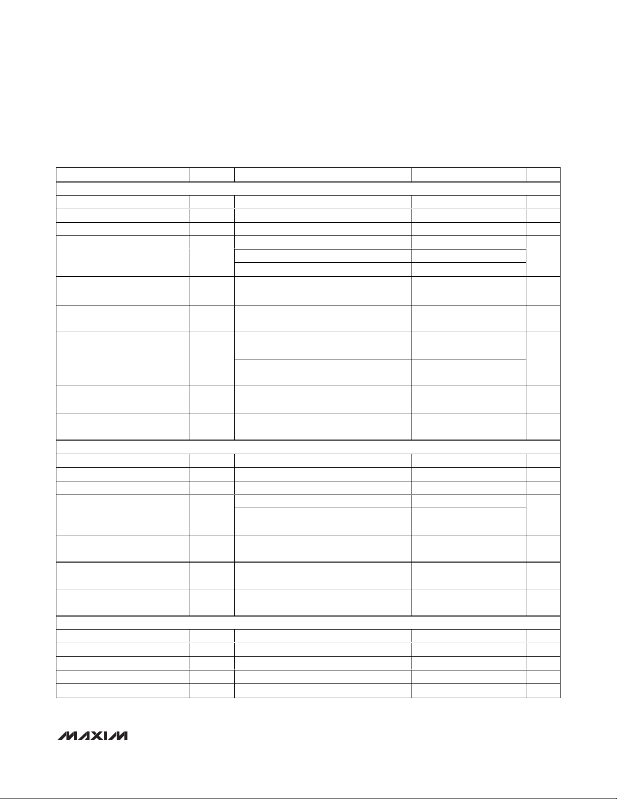
MAX16016/MAX16020/MAX16021
Low-Power µP Supervisory Circuits with
Battery-Backup Circuit and Chip-Enable Gating
_______________________________________________________________________________________ 3
ELECTRICAL CHARACTERISTICS (continued)
(VCC= 1.53V to 5.5V, V
BATT
= 3V, TA= -40°C to +85°C, unless otherwise noted. Typical values are at TA= +25°C.) (Note 2)
PARAMETER SYMBOL CONDITIONS MIN TYP MAX UNITS
RESET OUTPUT (RESET, RESET)
Reset Threshold V
VCC Falling to Reset Delay t
Reset Timeout Period t
RESET Output High Voltage
(Push-Pull Output)
RESET Output Leakage Current
(Open-Drain Output)
RESET Output Low Voltage V
RESET Output High Voltage
(Push-Pull Output)
RESET Output Leakage Current
(Open-Drain Output)
POWER-FAIL COMPARATOR
PFI, Input Threshold V
PFI, Hysteresis V
PFI Input Current VCC = 5.5V -1 +1 µA
PFO Output Low Voltage V
TH
VCC falling at 10V/ms 20 µs
RD
RP
VCC ≥ 3.3V, I
VCC ≥ 1.6V, I
OL
VCC ≥ 1.2V, I
V
VCC = 1.1 x VTH, I
OH
RESET deasserted
V
= 5.5V, RESET deasserted 1 µA
RESET
VCC ≥ 3.3V, I
= 3.2mA, RESET asserted 0.3
SINK
= 1mA, RESET asserted 0.3RESET Output Low Voltage V
SINK
= 100µA, RESET asserted 0.3
SINK
= 100µA,
SOURCE
= 3.2mA, RESET
SINK
(see Table 1) V
145 215 285 ms
V
OUT
- 0.3
deasserted
OL
VCC ≥ 1.8V, I
= 1.0mA, RESET
SINK
deasserted
V
OH
PFT
PFT-HYS
OL
VCC = 0.9 x VTH, I
RESET asserted
V
= 5.5V, RESET asserted 1 µA
RESET
VIN falling, 1.6V ≤ VCC ≤ 5.5V 0.572 0.590 0.611 V
VCC ≥ 1.6V, I
VCC ≥ 1.2V, I
= 1mA, output asserted 0.3
SINK
= 100µA, output asserted 0.3
SINK
SOURCE
= 100µA,
V
OUT
- 0.3
30 mV
0.3
0.3
V
V
V
V
V
PFO Output Voltage
High (Push-Pull Output)
V
PFO, Leakage Current
(Open-Drain Output)
PFO, Delay Time V
VCC = 1.1 x VTH, I
OH
asserted
V
SOURCE
= 100µA, output
V
OUT
- 0.3
= 5.5V, output deasserted 1 µA
PFO
+ 100mV to V
PFT
- 100mV 20 µs
PFT
MANUAL RESET (MR)
Input Low Voltage V
Input High Voltage V
IL
IH
0.7 x V
CC
0.3 x V
CC
Pullup Resistance 20 30 kΩ
Glitch Immunity VCC = 3.3V 100 ns
MR to Reset Delay 120 ns
V
V
V
Page 4
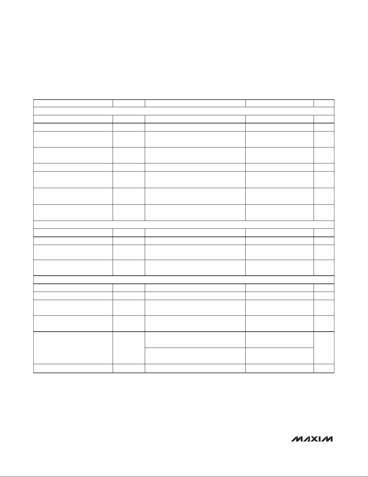
MAX16016/MAX16020/MAX16021
Low-Power µP Supervisory Circuits with
Battery-Backup Circuit and Chip-Enable Gating
4 _______________________________________________________________________________________
ELECTRICAL CHARACTERISTICS (continued)
(VCC= 1.53V to 5.5V, V
BATT
= 3V, TA= -40°C to +85°C, unless otherwise noted. Typical values are at TA= +25°C.) (Note 2)
PARAMETER SYMBOL CONDITIONS MIN TYP MAX UNITS
WATCHDOG TIMER (WDI, WDO)
Watchdog Timeout Period t
Minimum WDI Input Pulse Width t
WDI Input Low Voltage V
WDI Input High Voltage V
WDI Input Current (Note 7) V
WDO Output Low Voltage V
WDO Output High Voltage
(Push-Pull Output)
WDO Leakage Current
(Open-Drain Output)
BATTERY-ON INDICATOR (BATTON)
Output Low Voltage V
BATTON Leakage Current V
BATTON Output High Voltage V
Output Short-Circuit Current
(Note 4)
CE GATING (CEIN, CEOUT)
CEIN Leakage Current Reset asserted, VCC = 0.9 x VTH or 0V -1 +1 µA
CEIN to CEOUT Resistance Reset not asserted (Note 5) 8 50 Ω
CEOUT Short-Circuit Current
CEIN to CEOUT Propagation
Delay
Output High Voltage
Reset to CEOUT Delay 12 µs
0.83 1.235 1.64 s
320 ns
0.7 x
V
CC
V
OUT
- 0.3
V
OUT
- 0.3
0.75 2 mA
0.8 x
V
CC
V
-
BATT
0.1
V
WD
WDI
IL
IH
OL
OH
OL
OH
(Note 6)
(Note 6)
= 0 or 5.5V, time average -1 +1 µA
WDI
VCC = 1.1 x VTH, I
asserted
VCC = 1.1 x VTH, I
deasserted
= 5.5V, WDO deasserted 1 µA
V
WDO
I
= 3.2mA, V
SINK
= 5.5V 1 µA
BATTON
VCC = 0.9 x VTH, I
BATTON asserted
Sink current, V
Reset asserted, CEOUT = 0,
V
= 0.9 x V
CC
50Ω source, C
VCC = 5V, VCC ≥ V
V
= 0V, V
CC
TH
BATT
= 1mA, WDO
SINK
= 100µA, WDO
SOURCE
= 2.1V 0.3 V
BATT
= 100µA,
SOURCE
= 5V 60 mA
CC
= 50pF, VCC = 4.75V 1.5 7 ns
LOAD
BATT
≥ 2.2V I
, I
SOURCE
SOURCE
= 100µA
= 1µA
0.3 x
V
CC
0.3 V
V
V
V
V
V
Page 5
MAX16016/MAX16020/MAX16021
Low-Power µP Supervisory Circuits with
Battery-Backup Circuit and Chip-Enable Gating
_______________________________________________________________________________________ 5
Note 2: All devices are 100% production tested at TA= +25°C and TA= +85°C. Limits to -40°C are guaranteed by design.
Note 3: V
BATT
can be 0V anytime, or VCCcan go down to 0V if V
BATT
is active (except at startup).
Note 4: Use external current-limit resistor to limit current to 20mA (max).
Note 5: CEIN/CEOUT resistance is tested with V
CC
= 5V and V
CEIN
= 0V or 5V.
Note 6: WDI is internally serviced within the watchdog period if WDI is left unconnected.
Note 7: The WDI input current is specified as the average input current when the WDI input is driven high or low. The WDI input is
designed for a three-stated output device with a 10µA maximum leakage current and capable of driving a maximum capacitive load of 200pF. The three-state device must be able to source and sink at least 200µA when active.
ELECTRICAL CHARACTERISTICS (continued)
(VCC= 1.53V to 5.5V, V
BATT
= 3V, TA= -40°C to +85°C, unless otherwise noted. Typical values are at TA= +25°C.) (Note 2)
Table 1a. Reset Threshold Ranges
(MAX16016)
RESET THRESHOLD RANGES (V)
SUFFIX
MIN TYP MAX
L 4.508 4.63 4.906
M 4.264 4.38 4.635
T 2.991 3.08 3.239
S 2.845 2.93 3.080
R 2.549 2.63 2.755
Z 2.243 2.32 2.425
Y 2.117 2.19 2.288
W 1.603 1.67 1.733
V 1.514 1.575 1.639
Table 1b. Reset Threshold Ranges
(MAX16020/MAX16021)
RESET THRESHOLD RANGES (V)
SUFFIX
MIN TYP MAX
L 4.520 4.684 4.852
M 4.275 4.428 4.585
T 3.010 3.100 3.190
S 2.862 2.946 3.034
R 2.568 2.640 2.716
Z 2.260 2.323 2.390
Y 2.133 2.192 2.255
W 1.616 1.661 1.710
V 1.528 1.571 1.618
LOW LINE (LL)
Low Line to Reset Threshold
Voltage
VCC Falling to LL Delay VCC falling at 10V/ms 20 µs
LL Output Low Voltage V
LL Output High Voltage (Push-
Pull Output)
Output Leakage Current VLL = 5.5V, LL deasserted 1 µA
BATTERY-OK INDICATOR (BATTOK, BATT_TEST)
BATTOK Threshold Inferred internally from BATT 2.508 2.6 2.673 V
BATTOK Output Voltage Low V
BATTOK Output High Voltage V
BATTOK Output Leakage
Current
BATT_TEST Output Low Voltage VCC = 1.1 x VTH, I
PARAMETER SYMBOL CONDITIONS MIN TYP MAX UNITS
falling (see Table 2) mV
V
CC
OL
V
OH
OL
OH
VCC ≥ 1.6V, I
VCC ≥ 1.2V, I
VCC = 0.9 x V
LL deasserted
VCC = 1.1 x VTH, I
asserted
VCC = 1.1 x VTH, I
BATTOK asserted
V
= 5.5V, deasserted 1 µA
BATTOK
= 1mA, LL asserted 0.3
SINK
= 100µA, LL asserted 0.3
SINK
, I
TH_LL
SOURCE
SINK
SOURCE
SINK
= 100µA,
= 1mA, reset
= 100µA,
= 1mA 0.3 V
V
V
OUT
0.3
OUT
0.3
-
-
0.3 V
V
V
V
Page 6
MAX16016/MAX16020/MAX16021
Low-Power µP Supervisory Circuits with
Battery-Backup Circuit and Chip-Enable Gating
6 _______________________________________________________________________________________
Typical Operating Characteristics
(V
CC
= 5V, V
BATT
= 0V, TA= +25°C, unless otherwise noted.)
Table 2. Low-Line Threshold Ranges
LOW-LINE THRESHOLD RANGES (V)
SUFFIX
MIN TYP MAX
L 4.627 4.806
4.955
M 4.378 4.543
4.683
T 3.075 3.181 3.274
S
2.922
3.023
3.111
R
2.620
2.409
2.787
Z
2.309
2.383
2.450
Y
2.180
2.246
2.311
W
1.653
1.704
1.752
V
1.563
1.612
1.657
5
MAX16020PTEZ+
4
3
(µA)
CC
I
2
1
VCC SUPPLY CURRENT
vs. SUPPLY VOLTAGE
MAX16016 toc01
(µA)
CC
I
vs. TEMPERATURE (I
6
MAX16020PTEZ+
5
4
3
2
1
VCC SUPPLY CURRENT
OUT
= 0)
MAX16016 toc02
(µA)
BATT
I
0.7
0.6
0.5
0.4
0.3
0.2
0.1
BATT SUPPLY CURRENT
vs. SUPPLY VOLTAGE
MAX16020PTEZ+
= 2.5V
V
BATT
MAX16016 toc03
0
1.5 5.5
SUPPLY VOLTAGE (V)
5.04.54.03.53.02.52.0
BATTERY SUPPLY CURRENT
CC
= 0V)
MAX16016 toc04
(µA)
I
BATT
vs. TEMPERATURE (V
0.5
V
= +3.0V
BATT
0.4
0.3
0.2
0.1
0
-15 603510
-40 85
TEMPERATURE (°C)
0
-15 603510
-40 85
TEMPERATURE (°C)
BATT STANDBY CURRENT
vs. TEMPERATURE
5
VCC = 3.2V
4
= 3.0V
V
BATT
3
2
1
0
-1
-2
BATT STANDBY CURRENT (nA)
-3
-4
-5
-40 85
-15 603510
TEMPERATURE (°C)
MAX16016 toc05
0
05.52.01.5 4.03.52.5
4.0
MAX16020PTEZ+
3.5
3.0
2.5
2.0
1.5
TO OUT ON-RESISTANCE (Ω)
1.0
CC
V
0.5
0
1.5 5.55.03.5 4.54.0
SUPPLY VOLTAGE (V)
VCC TO OUT ON-RESISTANCE
vs. SUPPLY VOLTAGE
I
= 25mA
OUT
I
= 10mA
OUT
2.52.0 3.0
SUPPLY VOLTAGE (V)
5.03.00.5 4.51.0
MAX16016 toc06
Page 7
MAX16016/MAX16020/MAX16021
Low-Power µP Supervisory Circuits with
Battery-Backup Circuit and Chip-Enable Gating
_______________________________________________________________________________________
7
MAXIMUM
TRANSIENT
DURATION
(
)
Typical Operating Characteristics (continued)
(V
CC
= 5V, V
BATT
= 0V, TA= +25°C, unless otherwise noted.)
VCC TO OUT ON-RESISTANCE
5
VCC = +3.15V, I
4
3
2
TO OUT ON-RESISTANCE (Ω)
CC
1
V
0
-15 603510
-40 85
NORMALIZED RESET THRESHOLD
1.005
1.004
1.003
1.002
1.001
1.000
0.999
0.998
0.997
NORMALIZED RESET THRESHOLD
0.996
0.996
-15 603510
-40 85
WATCHDOG TIMEOUT PERIOD
1.5
1.4
1.3
1.2
1.1
1.0
0.9
0.8
0.7
WATCHDOG TIMEOUT PERIOD (s)
0.6
0.5
-15 603510
-40 85
vs. TEMPERATURE
= 65mA
OUT
TEMPERATURE (°C)
vs. TEMPERATURE
TEMPERATURE (°C)
vs. TEMPERATURE
TEMPERATURE (°C)
MAX16016 toc07
BATT TO OUT ON-RESISTANCE (Ω)
µs
MAX16016 toc10
0.65
0.64
MAX16016 toc13
0.63
0.62
0.61
0.60
0.59
PFI THRESHOLD (V)
0.58
0.57
0.56
0.55
BATT TO OUT ON-RESISTANCE
vs. TEMPERATURE (V
5
V
4
BATT
3
2
1
V
BATT
0
-15 603510
-40 85
MAXIMUM TRANSIENT DURATION
vs. RESET THRESHOLD OVERDRIVE
500
450
400
350
300
250
200
150
100
RESET OCCURS ABOVE THE CURVE
50
0
0400350200 300250
RESET THRESHOLD OVERDRIVE (mV)
-15 603510
-40 85
CC
V
= 2.5V
BATT
= 3V
= 4.5V
TEMPERATURE (°C)
10050 150
PFI THRESHOLD
vs. TEMPERATURE
V
PFI+
V
PFI-
TEMPERATURE (°C)
= 0V, I
OUT
MAX16020PTEZ+
= 20mA)
RESET OUTPUT VOLTAGE LOW
0.5
0.4
MAX16016 toc08
0.3
0.2
0.1
RESET OUTPUT VOLTAGE LOW (V)
0
020
210
MAX16020PTEZ+
208
206
MAX16016 toc11
204
202
200
198
196
RESET TIMEOUT PERIOD (ms)
194
192
190
-40 85
NORMALIZED LL THRESHOLD
1.005
1.004
1.003
MAX16016 toc14
1.002
1.001
1.000
0.999
0.998
NORMALIZED LL THRESHOLD
0.997
0.996
0.995
-40 85
vs. SINK CURRENT
MAX16016 toc09
VCC = 3.3V
VCC = 5V
18161412108642
SINK CURRENT (mA)
RESET TIMEOUT PERIOD
vs. TEMPERATURE
MAX16016 toc12
-15 603510
TEMPERATURE (°C)
vs. TEMPERATURE
MAX16016 toc15
-15 603510
TEMPERATURE (°C)
Page 8

MAX16016/MAX16020/MAX16021
Low-Power µP Supervisory Circuits with
Battery-Backup Circuit and Chip-Enable Gating
8 _______________________________________________________________________________________
Typical Operating Characteristics (continued)
(V
CC
= 5V, V
BATT
= 0V, TA= +25°C, unless otherwise noted.)
WDO OUTPUT VOLTAGE LOW
vs. SINK CURRENT
MAX16016 toc16
SINK CURRENT (mA)
WDO OUTPUT VOLTAGE LOW (V)
18161412108642
0.1
0.2
0.3
0.4
0.5
0
020
VCC = 3.3V
VCC = 5V
VCC SUPPLY CURRENT
vs. WDI FREQUENCY
MAX16016 toc17
WDI FREQUENCY (kHz)
I
CC
(µA)
10010
20
50
70
10
60
30
40
0
0 1000
BATTON OUTPUT VOLTAGE LOW
vs. SINK CURRENT
MAX16016 toc18
SINK CURRENT (mA)
BATTON OUTPUT VOLTAGE LOW (V)
18161412108642
0.1
0.2
0.3
0.4
0.5
0
020
VCC = 3.3V
VCC = 5V
BATTOK OUTPUT VOLTAGE LOW
vs. SINK CURRENT
0.5
0.4
0.3
0.2
0.1
BATTOK OUTPUT VOLTAGE LOW (V)
VCC = 5V
VCC = 3.3V
MAX16016 toc19
0
020
SINK CURRENT (mA)
RESET PROPAGATION DELAY
vs. THRESHOLD OVERDRIVE
70
MAX16020PTEZ+
60
50
40
30
20
PROPAGATION DELAY (µs)
10
0
0400
THRESHOLD OVERDRIVE (mV)
18161412108642
MAX16016 toc21
35030025020015010050
MR FALLING TO RESET DELAY
200ns/div
MAX16016 toc20
CHIP-ENABLE GATING LOCKING OUT
SIGNAL DURING RESET CONDITION
10µs/div
MAX16016 toc22
MR
5V/div
RESET
5V/div
RESET
5V/div
CEIN
5V/div
CEOUT
5V/div
Page 9

MAX16016/MAX16020/MAX16021
Low-Power µP Supervisory Circuits with
Battery-Backup Circuit and Chip-Enable Gating
_______________________________________________________________________________________ 9
Pin Description—MAX16016
PIN NAME FUNCTION
1VCCSupply Voltage Input. Bypass VCC to GND with a 0.1µF capacitor.
Backup Battery Input. If V
2 BATT
3 MR
4 PFI
5 WDI
6 BATTON Acti ve- H i g h Batter y- O n Outp ut. BATTON g oes hi g h w hen i n b atter y- b ackup m od e.
7 PFO
8 GND Ground
9 RESET
BATT. If V
capacitor.
Active-Low Manual Reset Input. RESET asserts when MR is pulled low. RESET remains low for the
duration of reset timeout period after MR transitions from low to high. Connect MR to OUT or leave
unconnected if not used. MR is internally connected to OUT through a 30kΩ pullup resistor.
Power-Fail Comparator Input. Connect PFI to a resistive divider to set the desired PFI threshold. The
PFI input is referenced to an internal V
immunity. The power-fail comparator is powered from OUT.
Watchdog Timer Input. If WDI remains high or low for longer than the watchdog timeout period (t
the internal watchdog timer runs out and a reset pulse is triggered for the reset timeout period. The
internal watchdog clears when reset asserts or whenever WDI sees a rising or falling edge. To
disable the watchdog feature, leave WDI unconnected or three-state the driver connected to WDI.
Active-Low Power-Fail Comparator Output. PFO goes low when V
threshold and goes high when V
Acti ve- Low Reset Outp ut. RESET asser ts w hen V
RESET r em ai ns l ow for the d ur ati on of the r eset ti m eout p er i od after V
and M R g oes hi g h. RESET al so asser ts l ow w hen the i nter nal w atchd og ti m er r uns out.
rises above 1.01 x V
CC
falls below its reset threshold, and if V
CC
, OUT connects to VCC. Bypass BATT to GND with a 0.1µF
BATT
threshold. A V
PFT
rises above V
PFI
C C
PFI-HYS
+ V
PFT
PFT-HYS
fal l s b el ow the r eset thr eshol d or M R i s p ul l ed l ow .
internal hysteresis provides noise
> VCC, OUT connects to
BATT
falls below the internal V
PFI
hysteresis.
r i ses ab ove the r eset thr eshol d
C C
PFT
WD
),
10 OUT
Switched Output. OUT is connected to V
greater than V
Bypass OUT
. OUT connects to BATT when RESET is asserted and V
BATT
to GND with a 0.1µF (min) capacitor.
when the reset output is not asserted or when VCC is
CC
is greater than VCC.
BATT
Page 10
MAX16016/MAX16020/MAX16021
Low-Power µP Supervisory Circuits with
Battery-Backup Circuit and Chip-Enable Gating
10 ______________________________________________________________________________________
Pin Description—MAX16020/MAX16021
PIN
MAX16020 MAX16021
1 1 BATT
22MR
3 3 PFI
4 4 WDI
NAME FUNCTION
Backup Battery Input. If V
connects to BATT. If V
GND with a 0.1µF capacitor.
Active-Low Manual Reset Input. RESET asserts when MR is pulled low. RESET remains low
for the duration of reset timeout period after MR transitions from low to high. Connect MR to
OUT or leave unconnected if not used. MR is internally connected to OUT through a 30kΩ
pullup resistor.
Power-Fail Comparator Input. Connect PFI to a resistive divider to set the desired PFI
threshold. The PFI input is referenced to an internal threshold V
hysteresis provides noise immunity. The power-fail comparator is powered from OUT.
Watchdog Timer Input. If WDI remains high or low for longer than the watchdog timeout
period (t
clears when reset asserts or whenever WDI sees a rising or falling edge. To disable the
watchdog feature, leave WDI unconnected or three-state the driver connected to WDI.
), the internal watchdog timer runs out and asserts WDO. The internal watchdog
WD
falls below its reset threshold, and if V
CC
rises above 1.01 x V
CC
BATT
> VCC, OUT
PFT
BATT
, V
PFI-HYS
internal
, OUT connects to VCC. Bypass BATT to
Active-Low Low-Line Output. LL goes low when V
55LL
6 — BATT_TEST
— 6 RESET
7 7 BATTOK
8 8 BATTON Active-High Battery-On Output. BATTON goes high when in battery-backup mode.
(Table 2). LL provides an early warning of V
to generate a nonmaskable interrupt (NMI) to initiate an orderly shutdown routine when
V
is falling.
CC
Open-Drain Battery-Test Output. Pulses low for 1.3s every 24 hours during the battery
voltage test. If V
load during the battery test.
Active-High Reset Output. RESET asserts when V
MR asserts and stays asserted for the reset timeout period after V
threshold and MR deasserts.
Battery-OK Output. BATTOK goes low when the battery voltage falls below the BATTOK
threshold (BATTOK is low when in battery-backup mode).
< 2.6V, BATTOK deasserts low. See Figure 6 for providing additional
BATT
CC
falls to 2.5% above the reset threshold
CC
failure before reset asserts. Use this output
falls below the reset threshold or when
CC
rises above the reset
CC
Page 11

MAX16016/MAX16020/MAX16021
Low-Power µP Supervisory Circuits with
Battery-Backup Circuit and Chip-Enable Gating
______________________________________________________________________________________ 11
Pin Description—MAX16020/MAX16021 (continued)
PIN
MAX16020 MAX16021
99WDO
10 10 PFO
11 11 GND Ground
12 12 RESET
13 13 OUT
14 14 CEOUT
15 15 CEIN Chip-Enable Input. The input to CE gating circuitry. Connect to GND or OUT if not used.
16 16 V
——EP
NAME FUNCTION
Active-Low Watchdog Output. WDO asserts when WDI remains high or low longer than the
watchdog timeout period. WDO returns high on the next WDI transition or when a reset is
asserted.
Active-Low Power-Fail Comparator Output. PFO goes low when V
CC
0.6V V
Active-Low Reset Output. RESET asserts when V
pulled low. RESET remains low for the duration of the reset timeout period after V
above the reset threshold and MR goes high.
Switched Output. OUT is connected to V
V
CC
greater than V
Active-Low Chip-Enable Output. CEOUT goes low only when CEIN is low and reset is not
asserted. If CEIN is low when reset is asserted, CEOUT stays low for 12µs (typ) or until
CEIN goes high, whichever occurs first.
Supply Voltage Input. Bypass V
Exposed Pad. Internally connected to GND. Connect EP to a large ground plane to aid
heat dissipation. Do not use EP as the only ground connection for the device.
threshold and goes high when V
PFT
is greater than V
. Bypass OUT to GND with a 0.1µF (min) capacitor.
CC
. OUT connects to BATT when RESET is asserted and V
BATT
to GND with a 0.1µF capacitor.
CC
rises above V
PFI
CC
when the reset output is not asserted or when
CC
falls below the internal
PFI
+ V
PFT
falls below the reset threshold or MR is
PFI-HYS
hysteresis.
CC
BATT
rises
is
Page 12
MAX16016/MAX16020/MAX16021
Low-Power µP Supervisory Circuits with
Battery-Backup Circuit and Chip-Enable Gating
12 ______________________________________________________________________________________
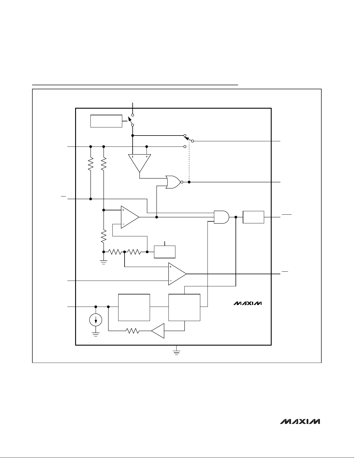
Functional Diagrams
BATT
BATTERY
FRESHNESS SEAL
V
CC
MR
RESET
OUT
REF
PFI
WDI
100nA
WATCHDOG
TRANSITION
DETECTOR
CLEAR
WATCHDOG
TIMER
DELAY
MAX16016
OUT
BATTON
RESET
PFO
25kΩ
GND
Page 13
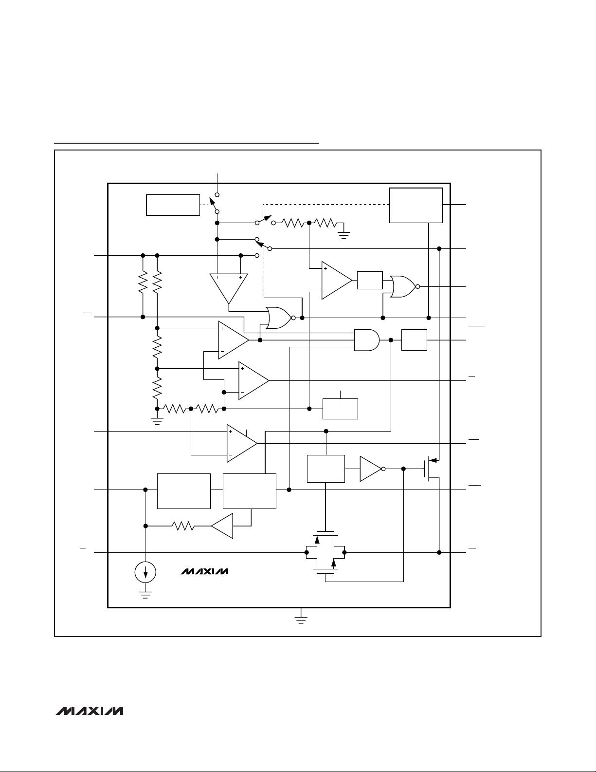
MAX16016/MAX16020/MAX16021
MAX16020
MAX16021
BATT
RESET
BATTERY
FRESHNESS SEAL
WATCHDOG
TIMER
BATTERY TEST
CIRCUIT
DISABLE
CE OUTPUT
CONTROL
REF
OUT
DELAY
LATCH
V
CC
OUT
BATTON
MR
PF1
OUT
PFO
CLEAR
WATCHDOG
TRANSITION
DETECTOR
RESET
(RESET)
(MAX16021
ONLY)
WDI
LL
WDO
GND
CEIN CEOUT
BATTOK
BATT_TEST
(MAX16020 ONLY)
100nA
25kΩ
Functional Diagrams (continued)
Low-Power µP Supervisory Circuits with
Battery-Backup Circuit and Chip-Enable Gating
______________________________________________________________________________________ 13
Page 14

MAX16016/MAX16020/MAX16021
Low-Power µP Supervisory Circuits with
Battery-Backup Circuit and Chip-Enable Gating
14 ______________________________________________________________________________________
Detailed Description
The
Typical Application Circuit
shows a typical connection using the MAX16020. OUT powers the static random-access memory (SRAM). If V
CC
is greater than the
reset threshold (VTH), or if V
CC
is lower than VTH, but
higher than V
BATT
, VCCconnects to OUT. If VCCis lower
than VTHand VCCis less than V
BATT
, BATT connects to
OUT (see the
Functional Diagrams
). In battery-backup
mode, an internal MOSFET connects the backup battery
to OUT. The on-resistance of the MOSFET is a function of
backup-battery voltage and temperature.
Backup-Battery Switchover
In a brownout or power failure, it may be necessary to
preserve the contents of the RAM. With a backup battery
installed at BATT, the MAX16016/MAX16020/MAX16021
automatically switch the RAM to the backup power when
VCCfalls. The MAX16016/MAX16020/MAX16021 have a
BATTON output that goes high when in battery-backup
mode. These devices require two conditions before
switching to battery-backup mode:
1) VCCmust be below the reset threshold.
2) VCCmust be below V
BATT
.
Table 3 lists the status of the inputs and outputs in battery-backup mode. The device does not power up if the
only voltage source is on BATT. OUT only powers up
from VCCat startup.
CE Signal Gating
The MAX16020/MAX16021 provide internal gating of
CE signals to prevent erroneous data from being written
to CMOS RAM in the event of a power failure or
brownout. During normal operation, the CE gate is
enabled and passes all CE transitions. When the reset
output asserts, this path becomes disabled, preventing
erroneous data from corrupting the CMOS RAM.
CEOUT is pulled up to OUT through an internal current
source. The 1.5ns propagation delay from CEIN to
CEOUT allows the devices to be used with most µPs
and high-speed DSPs.
During normal operation (reset not asserted), CEIN is
connected to CEOUT through a low on-resistance
transmission gate. If CEIN is high when a reset asserts,
CEOUT remains high regardless of any subsequent
transition on CEIN during the reset event.
If CEIN is low when reset asserts, CEOUT is held low
for 12µs to allow completion of the read/write operation.
After the 12µs delay expires, CEOUT goes high and
stays high regardless of any subsequent transitions on
CEIN during the reset event. When CEOUT is disconnected from CEIN, CEOUT is actively pulled up to OUT.
The propagation delay through the CE circuitry
depends on both the source impedance of the drive to
CEIN and the capacitive loading at CEOUT. Minimize
the capacitive load at CEOUT to minimize the propagation delay, and use a low output-impedance driver.
Low-Line Output (LL)
The low-line comparator monitors VCCwith a threshold
voltage typically 2.5% higher than the reset threshold
(see Table 2). LL asserts prior to a reset condition during
a brownout condition. On power-up, LL deasserts after
the reset output. LL can be used to provide a nonmaskable interrupt (NMI) to the µP when the voltage begins to
fall to initiate an orderly software shutdown routine.
Manual Reset Input
Many µP-based products require manual reset capability,
allowing the operator, a test technician, or external logic
circuitry to initiate a reset. For the MAX16016/MAX16020/
MAX16021, a logic-low on MR asserts RESET/RESET.
RESET/RESET remains asserted while MR is low. When
MR goes high RESET/RESET deasserts after a minimum
of 145ms (tRP). MR has an internal 30kΩ pullup resistor to
VCC. MR can be driven with TTL/CMOS logic levels or
with open-drain/collector outputs. Connect a normally
open momentary switch from MR to GND to create a
manual reset function; external debounce circuitry is not
required. If MR is driven from a long cable or the device is
used in a noisy environment, connect a 0.1µF capacitor
from MR to GND to provide additional noise immunity.
Table 3. Input and Output Status in
Battery-Backup Mode
PIN STATUS
V
CC
Disconnected from OUT
OUT Connected to BATT
BATT
Connected to OUT. Current drawn from the
battery is less than 0.55µA (at V
BATT
= 3V,
excluding I
OUT
) when VCC = 0V.
RESET/RESET
Asserted
BATTON, WDO
High state (push-pull), high impedance
(open-drain)
BATTOK, LL Low state
CEIN Disconnected from CEOUT
CEOUT Pulled up to V
OUT
PFO Not affected
Page 15

MAX16016/MAX16020/MAX16021
Low-Power µP Supervisory Circuits with
Battery-Backup Circuit and Chip-Enable Gating
______________________________________________________________________________________ 15
Watchdog Timer
Watchdog Input
The watchdog monitors µP activity through the input
WDI. If the µP becomes inactive, either the reset output is
asserted in pulses (MAX16016) or the watchdog output
goes low (MAX16020/MAX16021). To use the watchdog
function, connect WDI to a bus line or µP I/O line. If WDI
remains high or low for longer than the watchdog timeout
period, the internal watchdog timer runs out and RESET
asserts for the reset timeout period (MAX16016) or WDO
goes low (MAX16020/MAX16021). The internal watchdog
timer clears whenever the reset output asserts or the
WDI sees a rising or falling edge within the watchdog
timeout period. The WDI input is designed for a threestated output device with a 10µA maximum leakage current and the capability of driving a maximum capacitive
load of 200pF. The three-state device must be able to
source and sink at least 200µA when active. Disable the
watchdog timer by leaving WDI unconnected or by
three-stating the driver connected to WDI. The watchdog
timer periodically attempts to pulse WDI to the opposite
logic-level through a 25kΩ resistor for 40µs to determine
whether WDI is either unconnected or latched to a logic
state. The watchdog function is also disabled when in
battery-backup mode.
Watchdog Output
WDO remains high if there is a transition or pulse at WDI
during the watchdog-timeout period. WDO goes low if no
transition occurs at WDI during the watchdog timeout
period and remains low until the next transition at WDI or
when a reset is asserted. Connect WDO to MR to gener-
ate a system reset on every watchdog fault. When a
watchdog fault occurs in this mode, WDO goes low,
which pulls MR low, causing a reset pulse to be issued.
As soon as the reset output is asserted, the watchdog
timer clears and WDO returns high. With WDO connect-
ed to MR, a continuous high or low on WDI causes
145ms (min) reset pulses to be issued every 1.235s.
Battery Testing Function/BATTOK
Indicator (MAX16020/MAX16021)
The MAX16020/MAX16021 feature a battery testing
function that works in conjunction with the BATTOK output. The battery voltage is tested for 1.235s after V
CC
is
applied and once every 24 hours thereafter. During this
test, an internal 100kΩ resistor is connected from BATT
to ground and the battery is monitored to ensure that
the battery voltage is above 2.6V. If the battery voltage
is below 2.6V, the BATTOK output deasserts low to indicate a weak battery condition. The MAX16020 has a
BATT_TEST output that pulses high during the battery
voltage test. Connect a resistor and FET as shown in
Figure 6 to provide an additional load during the battery
test. In battery-backup mode, the battery testing function
is disabled and BATTOK goes low.
Battery Freshness Seal Mode
The MAX16016/MAX16020/MAX16021 battery freshness seal disconnects the backup battery from internal
circuitry and OUT until VCCis applied. This ensures the
backup battery connected to BATT is fresh when the
final product is used for the first time.
The internal freshness seal latch prevents BATT from
powering OUT until VCChas come up for the first time,
setting the latch. When VCCsubsequently turns off,
BATT begins to power OUT.
WDI
WDO
t
WD
t
WD
t
WD
Figure 1. Watchdog Timing (MAX16016/MAX16020)
Page 16
MAX16016/MAX16020/MAX16021
Low-Power µP Supervisory Circuits with
Battery-Backup Circuit and Chip-Enable Gating
16 ______________________________________________________________________________________
To reenable the freshness seal:
1) Connect a battery to BATT.
2) Bring V
CC
to 0V.
3) Drive MR higher than V
BATT
+ 1.2V for at least 3µs.
4) Pull OUT to 0V.
Reset Output
A µP’s reset input starts the µP in a known state. The
µP supervisory circuits assert a reset to prevent codeexecution errors during power-up, power-down, and
brownout conditions. Reset output is guaranteed to be
a logic-low or logic-high depending on the device chosen. RESET or RESET asserts when V
CC
is below the
reset threshold and remains asserted for at least 145ms
(tRP) after VCCrises above the reset threshold. RESET
or RESET also asserts when MR is low. The MAX16016
watchdog function causes RESET to assert in pulses
following a watchdog timeout. The reset output is available in both push-pull and open-drain configurations.
Power-Fail Comparator
The MAX16016/MAX16020/MAX16021 offer an undervoltage comparator that the output PFO goes low when
the voltage at PFI falls below its V
PFT
threshold.
Common uses for the power-fail comparator include
monitoring the power supply (such as a battery) before
any voltage regulation to provide an early power-fail
warning, so software can conduct an orderly system
shutdown. The power-fail comparator has a typical
input hysteresis of V
PFT-HYS
and is powered from OUT,
making it independent of the reset circuit. Connect the
PFI input to GND if not used.
Applications Information
Monitoring an Additional Supply
The MAX16016/MAX16020/MAX16021 µP supervisors
can monitor either positive or negative supplies using a
resistive voltage-divider to PFI. PFO can be used to
generate an interrupt to the µP or to trigger a reset
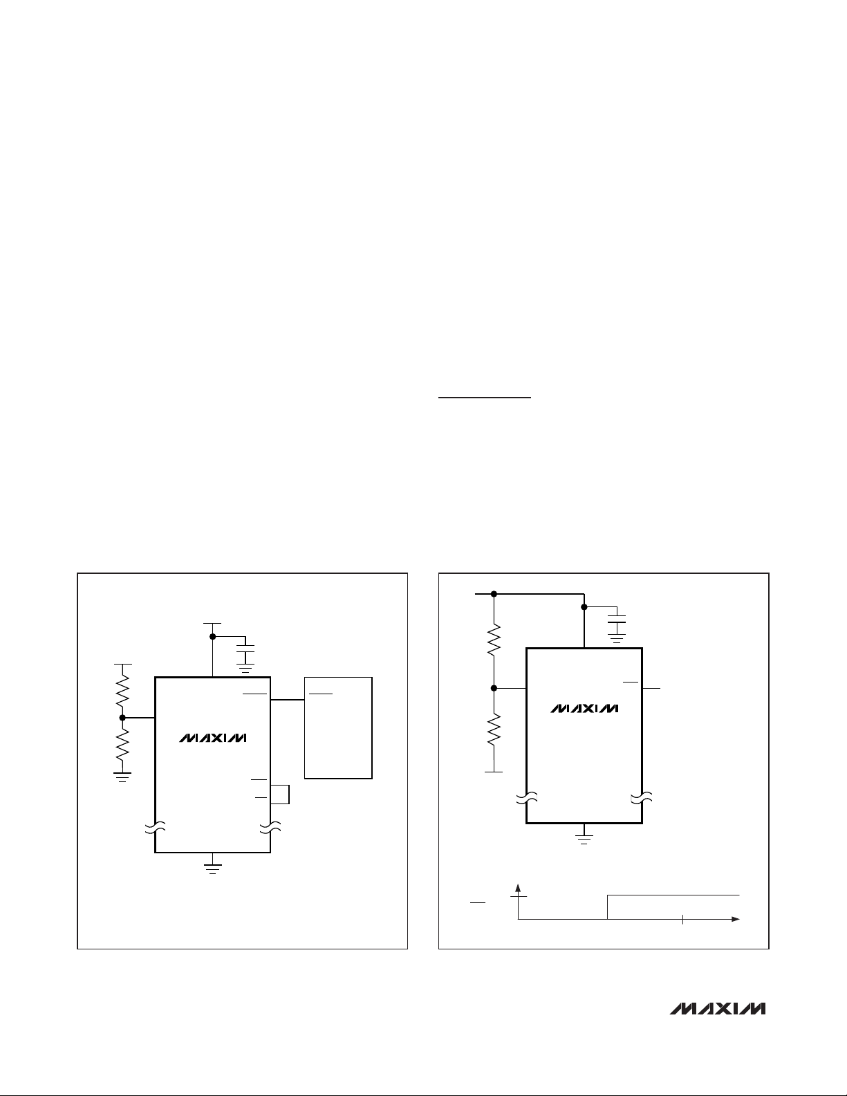
(Figures 2 and 3). To monitor a negative supply, connect the top of the resistive divider to V
CC
. Connect the
bottom of the resistive divider to the negative voltage to
be monitored.
MAX16016L
MAX16020L
MAX16021L
RESET RESET
PFO
MR
µP
GND
ADDITIONAL SUPPLY RESET VOLTAGE
R1+R2
R2
V
2(RESET)
= V
PFT
x
(—)
V
CC
PFI
0.1µF
V
1
R2
R1
V
2
Figure 2. Monitoring an Additional Supply by Connecting PFO
to MR
MAX16016
MAX16020
MAX16021
PFO
PFO
GND
R2
R1
V
TRIP
= V
PFT
- — (5 - V
PFT
)
V
TRIP
IS NEGATIVE
V
CC
PFI
0.1µF
R2
R1
5V
V-
0
+5V
V
TRIP
V-
0V
Figure 3. Monitoring a Negative Supply
Page 17

MAX16016/MAX16020/MAX16021
Low-Power µP Supervisory Circuits with
Battery-Backup Circuit and Chip-Enable Gating
______________________________________________________________________________________ 17
Figure 5. BATTON Driving an External Pass Transistor
Adding Hysteresis to PFI
The power-fail comparators have a typical input hysteresis of V
PFI-HYS
. This is sufficient for most applications where a power-supply line is being monitored
through an external voltage-divider (see the
Monitoring
an Additional Supply
section). Figure 4 shows how to
add hysteresis to the power-fail comparator. Select the
ratio of R1 and R2 so that PFI sees V
PFT
when VINfalls
to the desired trip point (V
TRIP
). Resistor R3 adds hysteresis. R3 is typically an order of magnitude greater
than R1 or R2. R3 should be larger than 50kΩ to prevent it from loading down PFO. Capacitor C1 adds
additional noise rejection.
Battery-On Indicator (Push-Pull Version)
BATTON goes high when in battery-backup mode. Use
BATTON to indicate battery-switchover status or to supply base drive to an external pass transistor for higher
current applications (Figure 5).
Operation Without a Backup Power Source
The MAX16016/MAX16020/MAX16021 provide a battery-backup function. If a backup power source is not
used, connect BATT to GND and OUT to VCC.
MAX16016L
MAX16020L
MAX16021L
PFO
GND
V
CC
PFI
0.1µF
R2
R1
R3
C1*
PFO
0
+5V
V
L
V
H
V
TRIP
V
IN
0.1µF
+5V
V
IN
TO µP
R1+R2
R2
V
TRIP
= V
PFT
x
(—)
*OPTIONAL
R1
R3
R1
R2
V
H
= (V
PFT
+ V
PFT_HYS
) x (– + – + 1
)
VCC - V
PFT
R3
V
PFT
R2
V
L
= R1 x
(
—
+
—
)
+ V
PFT
WHERE V
PFT
IS THE POWER-FAIL THRESHOLD VOLTAGE
Figure 4. Adding Hysteresis to the Power-Fail Comparator
V
CC
ADDRESS
DECODE
1µF
CE
CMOS RAM
A0–A15
µP
RESET
0.1µF
V
BATT
MR
BATTON
CC
MAX16020L
OUT
CEOUT
CEIN
RESET
GND
Page 18

MAX16016/MAX16020/MAX16021
Low-Power µP Supervisory Circuits with
Battery-Backup Circuit and Chip-Enable Gating
18 ______________________________________________________________________________________
Replacing the Backup Battery
When VCCis above VTH, the backup power source can
be removed without danger of triggering a reset pulse.
The device does not enter battery-backup mode when
V
CC
stays above the reset threshold voltage.
Negative-Going VCCTransients
The MAX16016/MAX16020/MAX16021 are relatively
immune to short duration, negative going VCCtransients. Resetting the µP when VCCexperiences only
small glitches is usually not desirable. A 0.1µF bypass
capacitor mounted close to VCCprovides additional
transient immunity.
MAX16020L
BATT
BATT_TEST
R
LOAD
V
CC
Figure 6. Adjustable BATT_TEST Load
Page 19

MAX16016/MAX16020/MAX16021
MAX16021
16
VCCCEIN
CEOUT
OUT
LL
RESET
BATTOK
BATTON
5
15
6
TQFN
14713
8
*EP
121
112
103
94
BATT
MR
PFI
WDI
RESET
GND
PFO
WDO
MAX16016
10
OUT
BATTON
V
CC
WDI
1
8
3
TDFN
+
+
7
RESETBATT
9
24
6
5
GND
PFO
MR
PFI
*EP
TOP VIEW
Pin Configurations (continued)
MAX16020L
CE
CEIN
GND
RAM
V
CC
PFO
BATT
0.1µF
R1
R2
0.1µF
0.1µF
CEOUT
OUT
RESET
ADDRESS
DECODE
RTC
µP
MR
A0–A15
RST
LL
NMI
WDI
I/O
WDO
I/O
SECONDARY
DC VOLTAGE
3.3V
PFI
0.1µF
(MIN)
V
CC
Typical Application Circuit
Low-Power µP Supervisory Circuits with
Battery-Backup Circuit and Chip-Enable Gating
______________________________________________________________________________________ 19
Page 20
MAX16016/MAX16020/MAX16021
Low-Power µP Supervisory Circuits with
Battery-Backup Circuit and Chip-Enable Gating
20 ______________________________________________________________________________________
Package Information
For the latest package outline information, go to
www.maxim-ic.com/packages
.
Selector Guide
Ordering Information (continued)
PART TEMP RANGE
PIN-PACKAGE
MAX16020_TE_+T -40°C to +85°C 16 TQFN-EP*
MAX16021_TE_+T -40°C to +85°C 16 TQFN-EP*
PACKAGE TYPE PACKAGE CODE DOCUMENT NO.
10 TDFN T1033-1
21-0137
16 TQFN T1644-4
21-0139
The first placeholder “_” designates all output options. Letter
“L” indicates push-pull outputs and letter “P” indicates opendrain outputs. The last placeholder “_” designates the reset
threshold (see Table 1).
T = Tape and reel.
+
Denotes a lead(Pb)-free/RoHS-compliant package.
*
EP = Exposed pad.
Chip Information
PROCESS: BiCMOS
ALL LOGIC
PART
MAX16016LTB_ Push-pull √√ WDI √ ———
MAX16016PTB_ Open-drain √√ WDI √ ———
MAX16020LTE_ Push-pull √√WDI/WDO √√
MAX16020PTE_ Open-drain √√WDI/WDO √√
MAX16021LTE_ Push-pull √√WDI/WDO √√
MAX16021PTE_ Open-drain √√WDI/WDO √√
OUTPUTS (EXCEPT
BATT_TEST)
MR
POWER-FAIL
COMPARATOR
WATCHDOG
TIMER
BATTON
LOW-
LINE
OUTPUT
BATTOK/
BATT_TEST/
RESET
BATTOK/
BATT_TEST
BATTOK/
BATT_TEST
BATTOK/
RESET
BATTOK/
RESET
CHIP-
ENABLE
√
√
√
√
Page 21

MAX16016/MAX16020/MAX16021
Low-Power µP Supervisory Circuits with
Battery-Backup Circuit and Chip-Enable Gating
Maxim cannot assume responsibility for use of any circuitry other than circuitry entirely embodied in a Maxim product. No circuit patent licenses are
implied. Maxim reserves the right to change the circuitry and specifications without notice at any time.
Maxim Integrated Products, 120 San Gabriel Drive, Sunnyvale, CA 94086 408-737-7600 ____________________
21
© 2008 Maxim Integrated Products is a registered trademark of Maxim Integrated Products, Inc.
Revision History
REVISION
NUMBER
0 5/08 Initial release —
1 7/08
2 9/08 Released the MAX16021. 20
3 12/08
REVISION
DATE
DESCRIPTION
Released the MAX16016. Updated Ordering Information, Electrical
Characteristics, Tables 1 and 2, Pin Description, and Detailed Description.
Updated Electrical Characteristics, Pin Description, Table 3, and the PowerFail Comparator section.
PAGES
CHANGED
1, 3, 4, 5, 9, 10, 12,
13, 15, 16, 19, 20
3, 9, 10, 11, 14, 16
 Loading...