

Page 1
General Description
The MAX16010–MAX16014 is a family of ultra-small, lowpower, overvoltage protection circuits for high-voltage,
high-transient systems such as those found in automotive,
telecom, and industrial applications. These devices operate over a wide 5.5V to 72V supply voltage range, making
them also suitable for other applications such as battery
stacks, notebook computers, and servers.
The MAX16010 and MAX16011 offer two independent
comparators for monitoring both undervoltage and
overvoltage conditions. These comparators offer opendrain outputs capable of handling voltages up to 72V.
The MAX16010 features complementary enable inputs
(EN/EN), while the MAX16011 features an active-high
enable input and a selectable active-high/low OUTB
output.
The MAX16012 offers a single comparator and an independent reference output. The reference output can be
directly connected to either the inverting or noninverting
input to select the comparator output logic.
The MAX16013 and MAX16014 are overvoltage protection circuits that are capable of driving two p-channel
MOSFETs to prevent reverse-battery and overvoltage
conditions. One MOSFET (P1) eliminates the need for
external diodes, thus minimizing the input voltage drop.
The second MOSFET (P2) isolates the load or regulates
the output voltage during an overvoltage condition. The
MAX16014 keeps the MOSFET (P2) latched off until the
input power is cycled.
The MAX16010 and MAX16011 are available in small
8-pin TDFN packages, while the MAX16012/MAX16013/
MAX16014 are available in small 6-pin TDFN packages.
These devices are fully specified from -40°C to +125°C.
Applications
Automotive
Industrial
48V Telecom/Server/Networking
FireWire
®
Notebook Computers
Multicell Battery-Stack Powered Equipment
Features
♦ Wide 5.5V to 72V Supply Voltage Range
♦ Open-Drain Outputs Up to 72V
(MAX16010/MAX16011/MAX16012)
♦ Fast 2µs (max) Propagation Delay
♦ Internal Undervoltage Lockout
♦ p-Channel MOSFET Latches Off After an
Overvoltage Condition (MAX16014)
♦ Adjustable Overvoltage Threshold
♦ -40°C to +125°C Operating Temperature Range
♦ Small 3mm x 3mm TDFN Package
MAX16010–MAX16014
Ultra-Small, Overvoltage Protection/
Detection Circuits
________________________________________________________________ Maxim Integrated Products 1
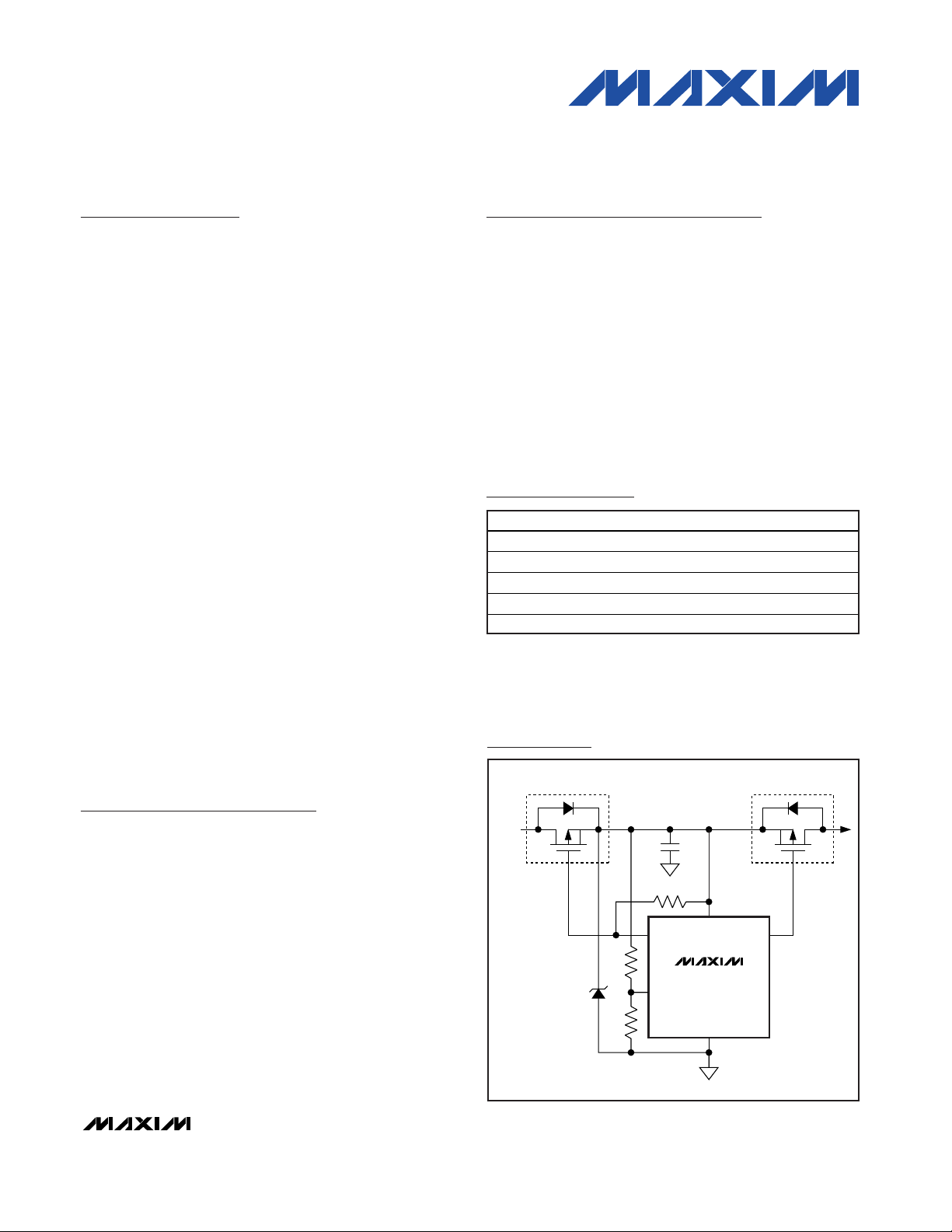
Ordering Information
MAX16013
MAX16014
GATE1
SET
GATE2
V
CC
GND
P1
R1
R2
V
BATT
P2
2MΩ*
*OPTIONAL
Typical Operating Circuit
19-3693; Rev 1; 12/05
For pricing, delivery, and ordering information, please contact Maxim/Dallas Direct! at
1-888-629-4642, or visit Maxim’s website at www.maxim-ic.com.
Note: Replace the “_” with “A” for 0.5% hysteresis, “B” for 5%
hysteresis, and “C” for 7.5% hysteresis.
FireWire is a registered trademark of Apple Computer, Inc.
Pin Configurations appear at end of data sheet.
PART* TEMP RANGE
PIN-PACKAGE
MAX16010TA_-T -40°C to +125°C 8 TDFN-8
MAX16011TA_-T -40°C to +125°C 8 TDFN-8
MAX16012TT-T -40°C to +125°C 6 TDFN-6
MAX16013TT-T -40°C to +125°C 6 TDFN-6
MAX16014TT-T -40°C to +125°C 6 TDFN-6
*Replace -T with +T for lead-free packages.
Page 2
MAX16010–MAX16014
Ultra-Small, Overvoltage Protection/
Detection Circuits
2 _______________________________________________________________________________________
ABSOLUTE MAXIMUM RATINGS
ELECTRICAL CHARACTERISTICS
(VCC= 14V, TA= -40°C to +125°C, unless otherwise noted. Typical values are at TA= +25°C.) (Note 1)
Stresses beyond those listed under “Absolute Maximum Ratings” may cause permanent damage to the device. These are stress ratings only, and functional
operation of the device at these or any other conditions beyond those indicated in the operational sections of the specifications is not implied. Exposure to
absolute maximum rating conditions for extended periods may affect device reliability.
(All pins referenced to GND, unless otherwise noted.)
V
CC
.........................................................................-0.3V to +80V
EN, EN, LOGIC...........................................-0.3V to (V
CC
+ 0.3V)
INA+, INB-, IN+, IN-, REF, SET ..............................-0.3V to +12V
OUTA, OUTB, OUT.................................................-0.3V to +80V
GATE1, GATE2 to V
CC
...........................................-12V to +0.3V
GATE1, GATE2...........................................-0.3V to (V
CC
+ 0.3V)
Current Sink/Source (all pins) .............................................50mA
Continuous Power Dissipation (T
A
= +70°C)
6-Pin TDFN (derate 18.2mW/°C above +70°C) .........1455mW
8-Pin TDFN (derate 18.2mW/°C above +70°C) .........1455mW
Operating Temperature Range .........................-40°C to +125°C
Maximum Junction Temperature .....................................+150°C
Storage Temperature Range .............................-60°C to +150°C
Lead Temperature (soldering, 10s) .................................+300°C
PARAMETER
SYMBOL
CONDITIONS
MIN
TYP
MAX
UNITS
Supply Voltage Range V
CC
5.5
V
VCC = 12V 20 30
Input Supply Current I
CC
No load
V
CC
= 48V 25 40
µA
VCC Undervoltage Lockout V
UVLO
VCC rising, part enabled, V
INA+
= 2V, OUTA
deasserted (MAX16010/MAX16011),
V
IN
= 2V, V
OUT
deasserted (MAX16012),
V
SET
= 0V, GATE2 = V
CLMP
(MAX16013/
MAX16014)
5
V
V
TH+
0.5% hysteresis, MAX16010/MAX16011
5.0% hysteresis, MAX16010/MAX16011/
MAX16013/MAX16014
INA+/INB-/SET Threshold Voltage
V
TH-
7.5% hysteresis MAX16010/MAX16011
V
MAX16010TAA/MAX16011TAA 0.5
MAX16010TAB/MAX16011TAB/
MAX16013/MAX16014
5.0
Threshold-Voltage Hysteresis
MAX16010TAC/MAX16011TAC 7.5
%
SET/IN_ Input Current SET/IN_ = 2V
nA
IN_ Operating Voltage Range 0 4 V
Startup Response Time t
START
VCC rising from 0 to 5.5V
µs
IN_ to OUT/SET to GATE2
Propagation Delay
t
PROP
IN_/SET rising from (VTH - 100mV) to
(V
TH
+ 100mV) or falling from (VTH +
100mV) to (V
TH
- 100mV) (no load)
2µs
VCC ≥ 5.5V, I
SINK
= 3.2mA 0.4 V
OUT_ Output-Voltage Low V
OL
VCC ≥ 2.8V, I
SINK
= 100µA 0.4 V
OUT_ Leakage Current I
LEAK
OUT_ = 72V 500 nA
72.0
4.75
1.215 1.245 1.265
1.21 1.223 1.26
1.15 1.18 1.21
1.12 1.15 1.18
-100 +100
100
5.25
Page 3
MAX16010–MAX16014
Ultra-Small, Overvoltage Protection/
Detection Circuits
_______________________________________________________________________________________ 3
ELECTRICAL CHARACTERISTICS (continued)
(VCC= 14V, TA= -40°C to +125°C, unless otherwise noted. Typical values are at TA= +25°C.) (Note 1)
PARAMETER
SYMBOL
CONDITIONS
MIN
TYP
MAX
UNITS
V
IL
0.4
EN/EN, LOGIC Input Voltage
V
IH
1.4
V
EN/EN, LOGIC Input Current 12µA
EN/EN, LOGIC Pulse Width 10 µs
VCC to GATE_ Output Low
Voltage
I
GATE_SINK
= 75µA, I
GATE_SOURCE
= 1µA,
V
CC
= 14V
711V
VCC to GATE_ Clamp Voltage VCC = 24V 12 18 V
MAX16012
Reference Output Voltage V
REF
No load
1.3
V
Reference Short-Circuit Current I
SHORT
REF = GND
µA
Sourcing, 0 ≤ I
REF
≤ 1µA 0.1
Reference Load Regulation
Sinking, -1µA ≤ I
REF
≤ 0 0.1
mV/µA
Input Offset Voltage VCM = 0 to 2V
mV
Input Offset Current 3nA
Input Hysteresis 8mV
Common-Mode Voltage Range CMVR 0 2.0 V
Common-Mode Rejection Ratio CMRR DC 70 dB
Comparator Power-Supply
Rejection Ratio
PSRR MAX16012, DC 70 dB
Note 1: 100% production tested at TA= +25°C and TA= +125°C. Specifications at TA= -40°C are guaranteed by design.
Typical Operating Characteristics
(V
IN
= 14V, TA = +25°C, unless otherwise noted.)
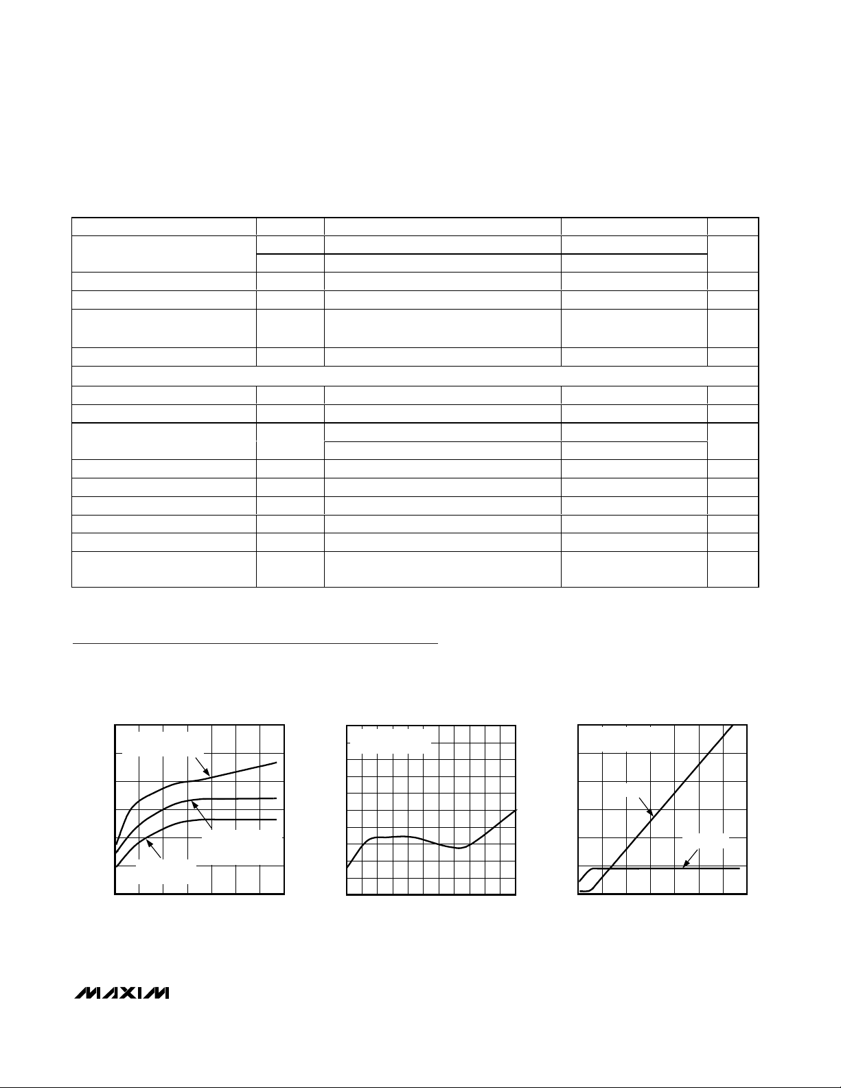
SUPPLY CURRENT
vs. SUPPLY VOLTAGE
MAX16010 toc01
SUPPLY VOLTAGE (V)
SUPPLY CURRENT (µA)
655545352515
15
20
25
30
35
40
10
575
MAX16013/MAX16014
SET = GND, EN = V
CC
MAX16010/MAX16011
INA+ = INB- = GND
OUTPUTS ENABLED
MAX16012
IN+ = IN- = GND
SUPPLY CURRENT
vs. TEMPERATURE
MAX16010 toc02
TEMPERATURE (°C)
SUPPLY CURRENT (µA)
1109565 80-10 5 20 35 50-25
26.05
26.10
26.15
26.20
26.25
26.30
26.35
26.40
26.45
26.50
26.00
-40 125
MAX16013/MAX16014
SET = GND, EN = V
CC
GATE VOLTAGE
vs. SUPPLY VOLTAGE
MAX16010 toc03
SUPPLY VOLTAGE (V)
GATE VOLTAGE (V)
655545352515
10
20
30
40
50
60
0
575
MAX16013/MAX16014
SET = GND, EN = V
CC
V
GATE
VCC - V
GATE
1.275
-12.5 +12.5
1.320
100
Page 4
MAX16010–MAX16014
Ultra-Small, Overvoltage Protection/
Detection Circuits
4 _______________________________________________________________________________________
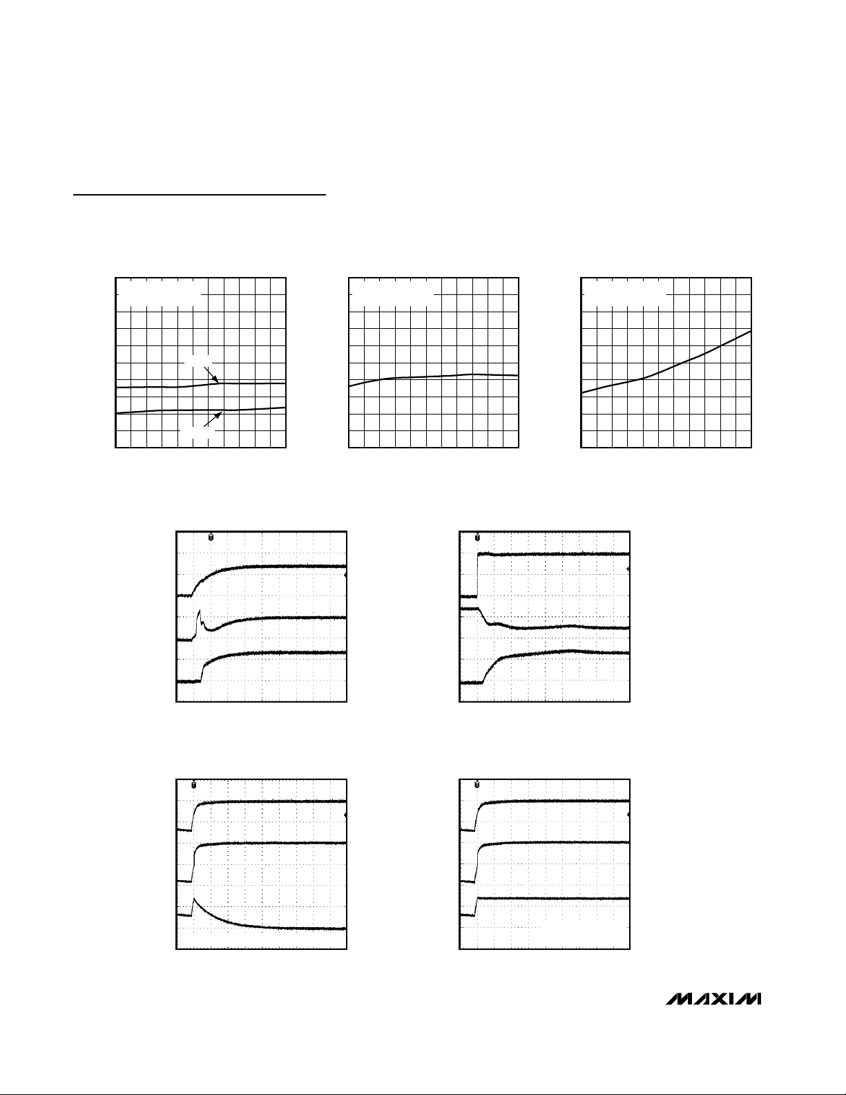
Typical Operating Characteristics (continued)
(V
IN
= 14V, TA = +25°C, unless otherwise noted.)
UVLO THRESHOLD
vs. TEMPERATURE
MAX16010 toc04
TEMPERATURE (°C)
UVLO THRESHOLD (V)
1109565 80-10 5 20 35 50-25
4.6
4.7
4.8
4.9
5.0
5.1
5.2
5.3
5.4
5.5
4.5
-40 125
INA+/INB-/SET = GND
EN = V
CC
RISING
FALLING
INA+/INB-/SET THRESHOLD
vs. TEMPERATURE
MAX16010 toc05
TEMPERATURE (°C)
INA+/INB-/SET THRESHOLD (V)
1109565 80-10 5 20 35 50-25
1.21
1.22
1.23
1.24
1.25
1.26
1.27
1.28
1.29
1.30
1.20
-40 125
INA+/INB-/SET RISING
EN = V
CC
GATE VOLTAGE
vs. TEMPERATURE
MAX16010 toc06
TEMPERATURE (°C)
(V
CC
- V
GATE
) (V)
1109565 80-10 5 20 35 50-25
9.1
9.2
9.3
9.4
9.5
9.6
9.7
9.8
9.9
10.0
9.0
-40 125
MAX16013/MAX16014
SET = GND, EN = V
CC
STARTUP WAVEFORM
(R
OUT
= 100Ω, CIN = 10µF, C
OUT
= 10nF)
MAX16010 toc07
V
GATE
5V/div
V
OUT
10V/div
V
CC
10V/div
200µs/div
STARTUP WAVEFORM
(R
OUT
= 100Ω, CIN = 10µF, C
OUT
= 10nF)
MAX16010 toc08
V
GATE
10V/div
V
OUT
10V/div
V
CC
1V/div
20µs/div
VEN = 0 TO 2V
OVERVOLTAGE SWITCH FAULT
(R
OUT
= 100Ω, CIN = 80µF, C
OUT
= 10nF)
MAX16010 toc09
V
GATE
20V/div
V
OUT
20V/div
V
CC
20V/div
1ms/div
VIN = 12V TO 40V, TRIP THRESHOLD = 28V
OVERVOLTAGE LIMIT
(R
OUT
= 100Ω, CIN = 80µF, C
OUT
= 10nF)
MAX16010 toc10
V
GATE
20V/div
V
OUT
20V/div
V
CC
20V/div
1ms/div
VIN = 12V TO 40V
TRIP THRESHOLD = 28V
Page 5

MAX16010–MAX16014
Ultra-Small, Overvoltage Protection/
Detection Circuits
_______________________________________________________________________________________ 5
Pin Description
PIN
MAX16010
MAX16011
MAX16012
MAX16013
MAX16014
NAME
FUNCTION
1
Positive-Supply Input Voltage. Connect VCC to a 5.5V to 72V supply.
2
Ground
3
EN
Active-Low Enable Input. Drive EN low to turn on the voltage detectors. Drive EN high to force the
OUTA and OUTB outputs low. EN is internally pulled up to V
CC
. Connect EN to GND if not used.
4
Open-Drain Monitor B Output. Connect a pullup resistor from OUTB to VCC. OUTB goes low when
INB- exceeds V
TH+
and goes high when INB- drops below V
TH-
(with LOGIC connected to GND for
the MAX16011). Drive LOGIC high to reverse OUTB’s logic state. OUTB is usually used as an
overvoltage output. OUTB goes low (LOGIC = low) or high (LOGIC = high) when V
CC
drops below
the UVLO threshold voltage.
5
Adjustable Voltage Monitor Threshold Input
6
EN
Active-High ENABLE Input. For the MAX16010/MAX16011, drive EN high to turn on the voltage
detectors. Drive EN low to force OUTA low and OUTB low (LOGIC = low) or high (LOGIC = high). For
the MAX16013/MAX16014, drive EN high to enhance the p-channel MOSFET (P2), and drive EN low
to turn off the MOSFET. EN is internally pulled down to GND. Connect EN to V
CC
if not used.
7
Open-Drain Monitor A Output. Connect a pullup resistor from OUTA to VCC. OUTA goes low when
INA+ drops below V
TH-
and goes high when INA+ exceeds V
TH+
. OUTA is usually used as an
undervoltage output. OUTA also goes low when V
CC
drops below the UVLO threshold voltage.
8
Adjustable Voltage Monitor Threshold Input
—
OUTB Logic-Select Input. Connect LOGIC to GND or VCC to configure the OUTB logic. See the
MAX16011 output logic table.
—
Open-Drain Comparator Output. Connect a pullup resistor from OUT to VCC. OUT goes low when
IN+ drops below IN-. OUT goes high when IN+ exceeds IN-.
—
IN- Inverting Comparator Input
—
Internal 1.30V Reference Output. Connect REF to IN+ for active-low output. Connect REF to IN- for
active-high output. REF can source and sink up to 1µA. Leave REF floating if not used. REF output is
stable with capacitive loads from 0 to 50pF.
—
Noninverting Comparator Input
—
Gate-Driver Output. Connect GATE2 to the gate of an external p-channel MOSFET pass switch.
GATE2 is driven low to the higher of V
CC
- 10V or GND during normal operations and quickly shorted
to V
CC
during an overvoltage condition (SET above the internal threshold). GATE2 is shorted to V
CC
when the supply voltage goes below the UVLO threshold voltage. GATE2 is shorted to VCC when EN
is low.
—
Device Overvoltage Threshold Adjustment Input. Connect SET to an external resistive divider network
to adjust the desired overvoltage disable or overvoltage limit threshold (see the Typical Application
Circuit and Overvoltage Limiter section).
—
Gate-Driver Output. Connect GATE1 to the gate of an external p-channel MOSFET to provide low
drop reverse voltage protection.
—
EP Exposed Pad. Connect EP to GND.
111V
2 22GND
———
4——OUTB
5——INB-
6—5
7——OUTA
8——INA+
3——LOGIC
—3—OUT
—4—
—5— REF
—6— IN+
—— 3GATE2
—— 4 SET
—— 6GATE1
———
CC
Page 6

MAX16010–MAX16014
Detailed Description
The MAX16010–MAX16014 is a family of ultra-small, lowpower, overvoltage protection circuits for high-voltage,
high-transient systems such as those found in automotive, telecom, and industrial applications. These devices
operate over a wide 5.5V to 72V supply voltage range,
making them also suitable for other applications such as
battery stacks, notebook computers, and servers.
The MAX16010 and MAX16011 offer two independent
comparators for monitoring both undervoltage and
overvoltage conditions. These comparators offer opendrain outputs capable of handling voltages up to 72V.
The MAX16010 features complementary enable inputs
(EN/EN), while the MAX16011 features an active-high
enable input and a selectable active-high/low OUTB
output.
The MAX16012 offers a single comparator and an independent reference output. The reference output can be
directly connected to either the inverting or noninverting input to select the comparator output logic.
The MAX16013 and MAX16014 are overvoltage protection circuits that are capable of driving two p-channel
MOSFETs to prevent reverse battery and overvoltage
conditions. One MOSFET (P1) eliminates the need for
external diodes, thus minimizing the input voltage drop.
While the second MOSFET (P2) isolates the load or regulates the output voltage during an overvoltage condition. The MAX16014 keeps the MOSFET (P2) latched
off until the input power is cycled.
Voltage Monitoring
The MAX16010/MAX16011 include undervoltage and
overvoltage comparators for window detection (see
Figure 1). OUT_ asserts high when the monitored voltage is within the selected “window.” OUTB asserts low
when the monitored voltage falls below the lower
(V
TRIPLOW
) limit of the window, or OUTA asserts low if
the monitored voltage exceeds the upper limit
(V
TRIPHIGH
). The application in Figure 1 shows OUT_
enabling the DC-DC converter when the monitored voltage is in the selected window.
The resistor values R1, R2, and R3 can be calculated
as follows:
where R
TOTAL
= R1 + R2 + R3.
Use the following steps to determine the values for R1,
R2, and R3.
1) Choose a value for R
TOTAL
, the sum of R1, R2, and
R3. Because the MAX16010/MAX16011 have very
high input impedance, R
TOTAL
can be up to 5MΩ.
2) Calculate R3 based on R
TOTAL
and the desired
upper trip point:
3) Calculate R2 based on R
TOTAL
, R3, and the desired
lower trip point:
4) Calculate R1 based on R
TOTAL
, R3, and R2:
R1 = R
TOTAL
- R2 - R3
The MAX16012 has both inputs of the comparator available with an integrated 1.30V reference (REF). When the
voltage at IN+ is greater than the voltage at IN- then OUT
goes high. When the voltage at IN- is greater than the
voltage at IN+ then OUT goes low. Connect REF to IN+
or IN- to set the reference voltage value. Use an external
resistive divider to set the monitored voltage threshold.
R
VR
V
R
TH TOTAL
TRIPLOW
23
=
×
−
−
R
VR
V
TH TOTAL
TRIPHIGH
3
=×
+
VV
R
R
TRIPHIGH TH
TOTAL
=
+
3
VV
R
RR
TRIPLOW TH
TOTAL
=+
−
23
Ultra-Small, Overvoltage Protection/
Detection Circuits
6 _______________________________________________________________________________________
MAX16010
DC-DC
REGULATOR
IN
EN
INA+
INB-
OUTB
OUTA
R3
R2
R1
+48V
EN
GND
V
CC
EN
Figure 1. MAX16010 Monitor Circuit
Page 7

The MAX16013/MAX16014 can be configured as an
overvoltage switch controller to turn on/off a load (see
the Typical Application Circuit). When the programmed
overvoltage threshold is tripped, the internal fast comparator turns off the external p-channel MOSFET (P2),
pulling GATE2 to VCCto disconnect the power source
from the load. When the monitored voltage goes below
the adjusted overvoltage threshold, the MAX16013
enhances GATE2, reconnecting the load to the power
source (toggle ENABLE on the MAX16014 to reconnect
the load). The MAX16013 can be configured as an
overvoltage limiter switch by connecting the resistive
divider to the load instead of VCC(Figure 3). See the
Overvoltage Limiter section.
Supply Voltage
Connect a 5.5V to 72V supply to VCCfor proper operation. For noisy environments, bypass VCCto GND with a
0.1µF or greater capacitor. When VCCfalls below the
UVLO voltage the following states are present (Table 1).
Hysteresis
Hysteresis adds noise immunity to the voltage monitors
and prevents oscillation due to repeated triggering
when the monitored voltage is near the threshold trip
voltage. The hysteresis in a comparator creates two trip
points: one for the rising input voltage (V
TH+
) and one
for the falling input voltage (V
TH-
). These thresholds are
shown in Figure 4.
Enable Inputs (EN or EN)
The MAX16011 offers an active-high enable input (EN),
while the MAX16010 offers both an active-high enable
input (EN) and active-low enable input (EN). For the
MAX16010, drive EN low or EN high to force the output
low. When the device is enabled (EN = high and EN =
low) the state of OUTA and OUTB depends on INA+
and INB- logic states.
MAX16010–MAX16014
Ultra-Small, Overvoltage Protection/
Detection Circuits
_______________________________________________________________________________________ 7
MAX16012
IN+
REF
IN-
OUT
R
PULLUP
R1
R2
GND
V
BATT
V
CC
OUT
Figure 2. Typical Operating Circuit for the MAX16012
MAX16013
GATE1
SET
GATE2
V
CC
GND
P2P1
R1
R2
V
BATT
Figure 3. Overvoltage Limiter Protection
Table 1. UVLO State (VCC< V
UVLO
)
PART
OUTA
OUTB
OUT
GATE2
MAX16010
Low — —
MAX16011
Low, LOGIC = low
——
MAX16012
——
—
MAX16013
MAX16014
———
High
Figure 4. Input and Output Waveforms
Low
Low
High, LOGIC = high
Low
V
HYST
V
TH+
V
IN+
V
TH-
V
CC
V
OUT
0V
t
PROP
t
PROP
t
PROP
Page 8

MAX16010–MAX16014
For the MAX16011, drive EN low to force OUTA low,
OUTB low when LOGIC = low, and OUTB high when
LOGIC = high. When the device is enabled (EN = high)
the state of OUTA and OUTB depends on the INA+,
INB-, and LOGIC input (see Table 2).
For the MAX16013/MAX16014, drive EN low to pull
GATE2 to VCC, turning off the p-channel MOSFET (P2).
When the device is enabled (EN = high), GATE2 is
pulled to the greater of (VCC- 10V) or GND turning on
the external MOSFET (P2).
Applications Information
Load Dump
Most automotive applications are powered by a multicell, 12V lead-acid battery with a voltage between 9V
and 16V (depending on load current, charging status,
temperature, battery age, etc.). The battery voltage is
distributed throughout the automobile and is locally
regulated down to voltages required by the different
system modules. Load dump occurs when the alternator is charging the battery and the battery becomes
disconnected. Power in the alternator inductance flows
into the distributed power system and elevates the voltage seen at each module. The voltage spikes have rise
times typically greater than 5ms and decays within several hundred milliseconds but can extend out to 1s or
more depending on the characteristics of the charging
system. These transients are capable of destroying
sensitive electronic equipment on the first fault event.
The MAX16013/MAX16014 provide the ability to disconnect the load from the charging system during an
overvoltage condition to protect the module. In addition, the MAX16013 can be configured in a voltage-limiting mode. This allows continuous operation while
providing overvoltage protection. See the Overvoltage
Limiter section.
Input Transients Clamping
When the external MOSFET is turned off during an
overvoltage occurrence, stray inductance in the power
path may cause voltage ringing to exceed the
MAX16013/MAX16014 absolute maximum input (VCC)
supply rating. The following techniques are recommended to reduce the effect of transients:
• Minimize stray inductance in the power path using
wide traces, and minimize loop area including the
power traces and the return ground path.
• Add a zener diode or transient voltage suppresser
(TVS) rated below VCCabsolute maximum rating
(Figure 3).
Overvoltage Limiter
When operating in overvoltage-limiter mode, the
MAX16013 drives the external p-channel MOSFET (P2),
resulting in the external MOSFET operating as a voltage
regulator.
During normal operation, GATE2 is pulled to the greater
of (VCC- 10V) or GND. The external MOSFET’s drain
voltage is monitored through a resistor-divider between
the P2 output and SET. When the output voltage rises
above the adjusted overvoltage threshold, an internal
comparator pulls GATE2 to VCC. When the monitored
voltage goes below the overvoltage threshold, the
p-channel MOSFET (P2) is turned on again. This
process continues to keep the voltage at the output regulated to within approximately a 5% window. The output
voltage is regulated during the overvoltage transients
and the MOSFET (P2) continues to conduct during the
overvoltage event, operating in switched-linear mode.
Caution must be exercised when operating the
MAX16013 in voltage-limiting mode for long durations
due to the MOSFET’s power dissipation consideration
(see the MOSFET Selection and Operation section).
MOSFET Selection and Operation
(MAX16013 and MAX16014)
Most battery-powered applications must include reverse
voltage protection. Many times this is implemented with a
diode in series with the battery. The disadvantage in
using a diode is the forward voltage drop of the diode,
which reduces the operating voltage available to downstream circuits (V
LOAD
= V
BATTERY
- V
DIODE
). The
MAX16013 and MAX16014 include high-voltage GATE1
drive circuitry allowing users to replace the high-voltagedrop series diode with a low-voltage-drop MOSFET
device (as shown in the Typical Operating Circuit and
Figure 3). The forward voltage drop is reduced to I
LOAD
x R
DS-ON
of P1. With a suitably chosen MOSFET, the
voltage drop can be reduced to millivolts.
Ultra-Small, Overvoltage Protection/
Detection Circuits
8 _______________________________________________________________________________________
Table 2. MAX16011 Output Logic
LOGIC
INA+ INB- OUTA OUTB
Low
High
Low
Low
Low
High
Impedance
High
High
High
Impedance
High
Low Low
> V
< V
> V
< V
TH+
TH-
TH+
TH-
> V
< V
> V
< V
TH+
TH-
TH+
TH-
Impedance
Impedance
Page 9

In normal operating mode, internal GATE1 output circuitry enhances P1 to a 10V gate-to-source (VGS) for
11V < VCC< 72V. The constant 10V enhancement
ensures P1 operates in a low R
DS-ON
mode, but the
gate-source junction is not overstressed during highbattery-voltage application or transients (many MOSFET
devices specify a ±20V VGSabsolute maximum). As
VCCdrops below 10V GATE1 is limited to GND, reducing P1 VGSto VCC- GND. In normal operation the P1
power dissipation is very low:
P1 = I
LOAD
2
x R
DS-ON
During reverse-battery applications, GATE1 is limited to
GND and the P1 gate-source junction is reverse
biased. P1 is turned off and neither the MAX16013/
MAX16014 nor the load circuitry is exposed to the
reverse-battery voltage. Care should be taken to place
P1 (and its internal drain-to-source diode) in the correct
orientation for proper reverse battery operation.
P2 protects the load from input overvoltage conditions.
During normal operating modes (the monitored voltage
is below the adjusted overvoltage threshold), internal
GATE2 output circuitry enhances P2 to a 10V gate-tosource (VGS) for 11V < VCC< 72V. The constant 10V
enhancement ensures P2 operates in a low R
DS-ON
mode but the gate-to-source junction is not overstressed during high-battery-voltage applications
(many pFET devices specify a ±20V VGSabsolute maximum). As VCCdrops below 10V, GATE2 is limited to
GND, reducing P2 V
GS
to VCC- GND. In normal opera-
tion, the P2 power dissipation is very low:
P2 = I
LOAD
2
x R
DS-ON
During overvoltage conditions, P2 is either turned completely off (overvoltage-switch mode) or cycled off-onoff (voltage-limiter mode). Care should be taken to
place P2 (and its internal drain-to-source diode) in the
correct orientation for proper overvoltage protection
operation. During voltage-limiter mode, the drain of P2
is limited to the adjusted overvoltage threshold, while
the battery (VCC) voltage rises. During prolonged overvoltage events, P2 temperature can increase rapidly
due to the high power dissipation. The power dissipated by P2 is:
P2 = V
DS-P2
x I
LOAD
= (VCC- V
OV-ADJUSTED
) x I
LOAD
where VCC~ V
BATTERY
and V
OV-ADJUSTED
is the desired
load limit voltage. For prolonged overvoltage events with
high P2 power dissipation, proper heatsinking is required.
Adding External Pullup Resistors
It may be necessary to add an external resistor from
VCCto GATE1 to provide enough additional pullup
capability when the GATE1 input goes high. The
GATE_ output can only source up to 1µA current. If the
source current is less than 1µA, no external resistor
may be necessary. However, to improve the pullup
capability of the GATE_ output when it goes high, connect an external resistor between VCCand the GATE_.
The application shows a 2MΩ resistor, which is large
enough not to impact the sinking capability of the
GATE_ (during normal operation) while providing
enough pullup during an overvoltage event. With an
11V (worst case) VCC-to-gate clamp voltage and a
sinking current of 75µA, the smallest resistor should be
11V/75µA, or about 147kΩ. However, since the GATE_
is typically low most of the time, a higher value should
be used to reduce overall power consumption.
MAX16010–MAX16014
Ultra-Small, Overvoltage Protection/
Detection Circuits
_______________________________________________________________________________________ 9
Page 10

MAX16010–MAX16014
Ultra-Small, Overvoltage Protection/
Detection Circuits
10 ______________________________________________________________________________________
Functional Diagrams
MAX16010
HYST
HYST
REGULATOR
ENABLE CIRCUITRY
1.23V
~4V
INA+
INB-
OUTA
OUTB
GND EN
EN
V
CC
Figure 5. MAX16010 Functional Diagram
MAX16011
HYST
HYST
REGULATOR
ENABLE
CIRCUITRY
OUTB
LOGIC
1.23V
~4V
INA+
INB-
OUTA
OUTB
GND EN
LOGIC
V
CC
Figure 6. MAX16011 Functional Diagram
MAX16012
REGULATOR
1.23V
~4V
IN-
OUT
GND
V
CC
IN+
REF
Figure 7. MAX16012 Functional Diagram
MAX16013
MAX16014
HYST
ENABLE
CIRCUITRY
LATCH
CLEAR
1.23V
SET
GND EN
V
CC
GATE1
GATE2
Figure 8. MAX16013/MAX16014 Functional Diagram
Page 11

MAX16010–MAX16014
Ultra-Small, Overvoltage Protection/
Detection Circuits
______________________________________________________________________________________ 11
Chip Information
PROCESS: BiCMOS
8765
1234
INA+ OUTA EN INB-
V
CC
GND EN OUTB
TOP VIEW
MAX16010
TDFN (3mm x 3mm)
8765
1234
INA+ OUTA EN INB-
V
CC
GND LOGIC OUTB
MAX16011
TDFN (3mm x 3mm)
6
IN+
5
REF
4
IN-
1
V
CC
2
GND
3
OUT
MAX16012
TDFN (3mm x 3mm)
6
GATE1
5
EN
4
SET
1
V
CC
2
GND3GATE2
MAX16013
MAX16014
TDFN (3mm x 3mm)
Pin Configurations
Page 12

MAX16010–MAX16014
Ultra-Small, Overvoltage Protection/
Detection Circuits
Maxim cannot assume responsibility for use of any circuitry other than circuitry entirely embodied in a Maxim product. No circuit patent licenses are
implied. Maxim reserves the right to change the circuitry and specifications without notice at any time.
12 ____________________Maxim Integrated Products, 120 San Gabriel Drive, Sunnyvale, CA 94086 408-737-7600
© 2005 Maxim Integrated Products Printed USA is a registered trademark of Maxim Integrated Products, Inc.
6, 8, &10L, DFN THIN.EPS
L
C
L
C
PIN 1
INDEX
AREA
D
E
L
e
L
A
e
E2
N
G
1
2
21-0137
PACKAGE OUTLINE, 6,8,10 & 14L,
TDFN, EXPOSED PAD, 3x3x0.80 mm
-DRAWING NOT TO SCALE-
k
e
[(N/2)-1] x e
REF.
PIN 1 ID
0.35x0.35
DETAIL A
b
D2
A2
A1
COMMON DIMENSIONS
SYMBOL
MIN. MAX.
A
0.70 0.80
D 2.90 3.10
E
2.90 3.10
A1
0.00 0.05
L
0.20 0.40
PKG. CODE
N
D2 E2 e
JEDEC SPEC
b
[(N/2)-1] x e
PACKAGE VARIATIONS
0.25 MIN.k
A2 0.20 REF.
2.30±0.101.50±0.106T633-1 0.95 BSC MO229 / WEEA 1.90 REF0.40±0.05
1.95 REF0.30±0.05
0.65 BSC
2.30±0.108T833-1
2.00 REF0.25±0.05
0.50 BSC
2.30±0.1010T1033-1
2.40 REF0.20±0.05- - - -
0.40 BSC
1.70±0.10 2.30±0.1014T1433-1
1.50±0.10
1.50±0.10
MO229 / WEEC
MO229 / WEED-3
0.40 BSC
- - - - 0.20±0.05 2.40 REFT1433-2 14 2.30±0.101.70±0.10
T633-2 6 1.50±0.10 2.30±0.10 0.95 BSC
MO229 / WEEA
0.40±0.05 1.90 REF
T833-2 8 1.50±0.10 2.30±0.10
0.65 BSC MO229 / WEEC
0.30±0.05 1.95 REF
T833-3 8 1.50±0.10 2.30±0.10
0.65 BSC MO229 / WEEC
0.30±0.05 1.95 REF
-DRAWING NOT TO SCALE-
G
2
2
21-0137
PACKAGE OUTLINE, 6,8,10 & 14L,
TDFN, EXPOSED PAD, 3x3x0.80 mm
DOWNBONDS
ALLOWED
NO
NO
NO
NO
YES
NO
YES
NO
Package Information
(The package drawing(s) in this data sheet may not reflect the most current specifications. For the latest package outline information,
go to www.maxim-ic.com/packages
.)
 Loading...