

Page 1
For pricing delivery, and ordering information please contact Maxim/Dallas Direct! at
1-888-629-4642, or visit Maxim’s website at www.maxim-ic.com.
1
2
3
4
8
7
6
5
OUT
CXP
CXN
PGNDGND
IN
SHDN
AOUT
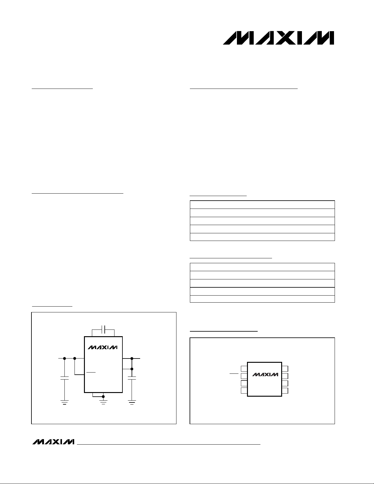
MAX1595
µMAX
TOP VIEW
OUTPUT
OUT
IN
INPUT
SHDN
GND
CXN CXP
PGND
AOUT
MAX1595
MAX1595
Regulated 3.3V/5.0V Step-Up/Step-Down
Charge Pump
Maxim Integrated Products 1
Typical Operating Circuit
19-2107; Rev 1; 8/02
General Description
The MAX1595 charge-pump regulator generates either
3.3V or 5V from a 1.8V to 5.5V input. The unique control
architecture allows the regulator to step up or step
down the input voltage to maintain output regulation.
The 1MHz switching frequency, combined with a
unique control scheme, allows the use of a ceramic
capacitor as small as 1µF for 125mA of output current.
The complete regulator requires three external capacitors—no inductor is needed. The MAX1595 is specifically designed to serve as a high-power, highefficiency auxiliary supply in applications that demand
a compact design. The MAX1595 is offered in spacesaving 8-pin µMAX and high-power 12-pin thin QFN
packages.
Applications
White LED Power
Flash Memory Supplies
Battery-Powered Applications
Miniature Equipment
PCMCIA Cards
3.3V to 5V Local Conversion Applications
Backup-Battery Boost Converters
3V to 5V GSM SIMM Cards
Features
♦ Ultra-Small: Requires Only Three Ceramic
Capacitors
♦ No Inductors Required
♦ Up to 125mA Output Current
♦ Regulated ±3% Output Voltage
♦ 1MHz Switching Frequency
♦ 1.8V to 5.5V Input Voltage
♦ 220µA Quiescent Current
♦ 0.1µA Shutdown Current
♦ Load Disconnect in Shutdown
Ordering Information
Pin Configurations continued at end of data sheet.
Selector Guide
*Contact factory for other fixed-output voltages from 2.7V to 5.0V.
Pin Configurations
PART TEMP RANGE PIN-PACKAGE
MAX1595EUA33 -40°C to +85°C
MAX1595ETC33
MAX1595EUA50
MAX1595ETC50
PART V
MAX1595EUA33 3.3V
MAX1595ETC33
MAX1595EUA50
MAX1595ETC50
8 µMAX
-40°C to +85°C
-40°C to +85°C
-40°C to +85°C
* TOP M ARK
OUT
3.3V
5.0V
5.0V
12 Thin QFN
8 µMAX
12 Thin QFN
AAAP
AAAM
—
—
Page 2
MAX1595
Regulated 3.3V/5.0V Step-Up/Step-Down
Charge Pump
2 _______________________________________________________________________________________
ABSOLUTE MAXIMUM RATINGS
ELECTRICAL CHARACTERISTICS
(VIN= 2V for MAX1595_ _ _33, VIN= 3V for MAX1595_ _ _50, CIN= 1µF, CX= 0.22µF, C
OUT
= 1µF, TA= -40° to +85°C, unless otherwise
noted. Typical values are at T
A
= +25°C.) (Note 1)
Stresses beyond those listed under “Absolute Maximum Ratings” may cause permanent damage to the device. These are stress ratings only, and functional
operation of the device at these or any other conditions beyond those indicated in the operational sections of the specifications is not implied. Exposure to
absolute maximum rating conditions for extended periods may affect device reliability.
IN, OUT, AOUT to GND............................................-0.3V to +6V
SHDN to PGND ........................................................-0.3V to +6V
PGND to GND .......................................................-0.3V to +0.3V
CXN to PGND.....................-0.3V to (Lower of IN + 0.8V or 6.3V)
CXP to GND ................................-0.8V to (Higher of OUT + 0.8V
or IN + 0.8V but not greater than 6V)
Continuous Output Current ...............................................150mA
Continuous Power Dissipation (T
A
= +70°C)
8-Pin µMAX (derate 4.5mW/°C above +70°C) ............362mW
12-Pin Thin QFN (derate 18.5mW/°C
above +70°C)............................................................1481mW
Operating Temperature Range ...........................-40°C to +85°C
Junction Temperature......................................................+150°C
Storage Temperature Range .............................-65°C to +150°C
Lead Temperature (soldering, 10s) .................................+300°C
Note 1: Specifications to -40°C are guaranteed by design, not production tested.
Input Voltage Range V
Input Undervoltage Lockout
Threshold
Input Undervoltage Lockout
Hysteresis
Output Voltage V
No-Load Input Current I
Switching Frequency f
Shutdown Supply Current I
SHDN Input Voltage Low V
SHDN Input Voltage High V
SHDN Input Leakage Current 0.1 µA
PARAMETER SYMBOL CONDITIONS MIN TYP MAX UNITS
IN
OUT
Q
OSC
SHDN
IN L
IN H
0 < I
V
0 < I
= +2.0V
0 < I
= +1.8V
VIN = +2.0V, MAX1595_ _ _33 220 320
VIN = +3.0V, MAX1595_ _ _50 240 350
I
L OA D
SHDN = 0, VIN = +5.5V, V
VIN = 2.0V to 5.5V 0.6 V
VIN = 2.0V to 5.5V 1.6 V
L OA D
= + 3.0V
I N
LOAD
LOAD
> 20m A, V
< 125m A,
< 75mA, V
< 30mA, V
OU T
TA = 0 to +85°C 4.85 5.05 5.15
T
= -40°C to +85°C 4.80 5.20
A
TA = 0 to +85°C 3.20 3.33 3.40
IN
= -40°C to +85°C 3.16 3.44
T
A
TA = 0 to +85°C 3.20 3.33 3.40
IN
= -40°C to +85°C 3.16 3.44
T
A
> V
IN
= 0 5 µA
OUT
1.8 5.5 V
1.40 1.60 1.72 V
40 mV
0.85 1.0 1.15 MHz
V
µA
Page 3
MAX1595
Regulated 3.3V/5.0V Step-Up/Step-Down
Charge Pump
_______________________________________________________________________________________ 3
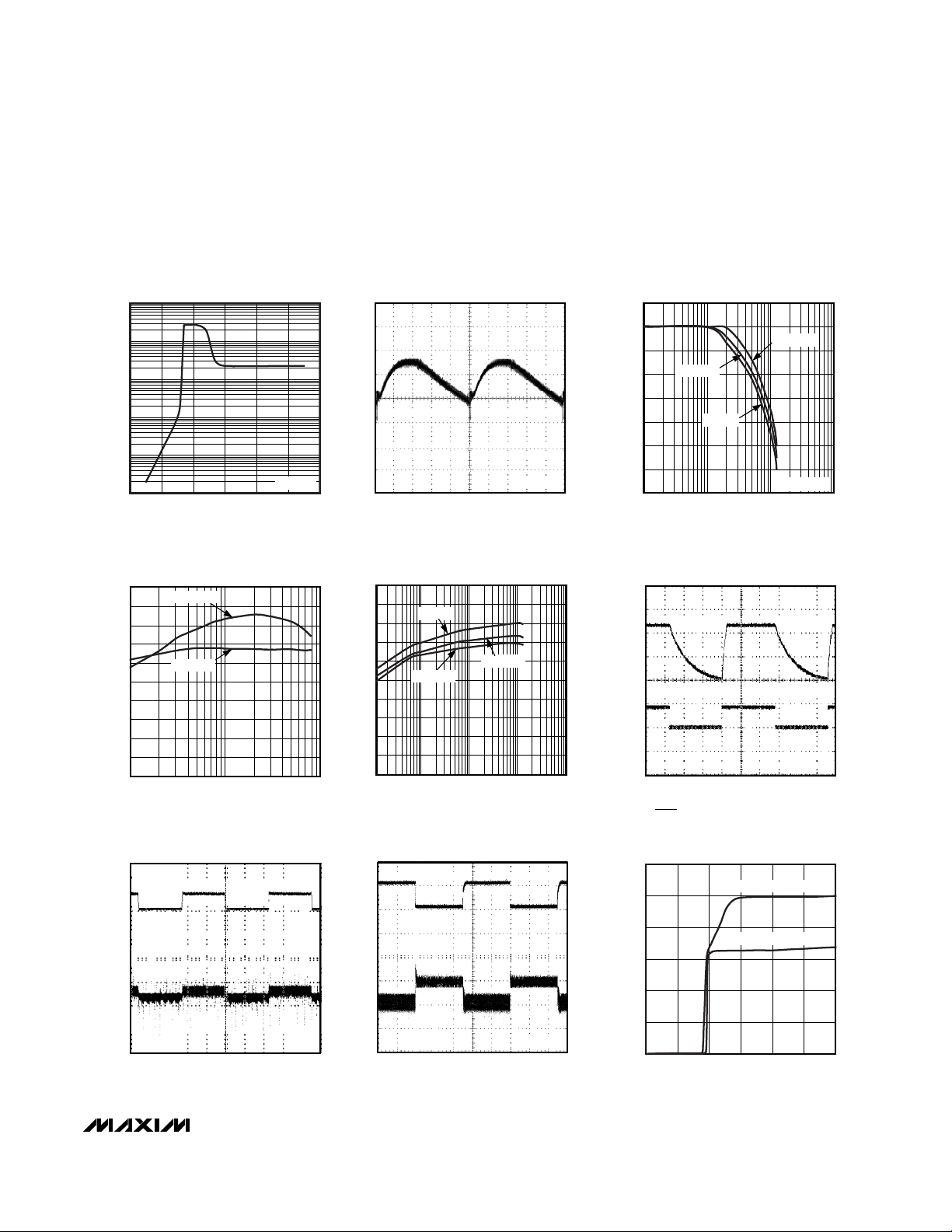
__________________________________________Typical Operating Characteristics
(Circuit of Figure 4, VIN= 2V for MAX1595_ _ _33, VIN= 3V for MAX1595_ _ _50, TA = +25°C, unless otherwise noted.)
0.1
10
1
1000
100
10000
021345
NO LOAD SUPPLY CURRENT
vs. SUPPLY VOLTAGE
MAX1595 toc01
SUPPLY VOLTAGE (V)
SUPPLY CURRENT (µA)
6
V
OUT
= 5V
200ns/div
OUTPUT WAVEFORM
50mV/div
MAX1595 toc02
OUTPUT WAVEFORM. AC-COUPLED.
V
IN
= 3.6V, I
LOAD
= 100mA, C
OUT
= 1µF
V
OUT
= 5V
4.90
5.00
4.98
4.96
4.94
4.92
5.06
1 10 100
1000
OUTPUT VOLTAGE
vs. LOAD CURRENT
MAX1595 toc03
LOAD CURRENT (mA)
OUTPUT VOLTAGE (V)
5.04
5.02
VIN = 3V
VIN = 3.6V
VIN = 3.3V
V
OUT
= 5V
100
0
1 10 100
3V EFFICIENCY
vs. LOAD CURRENT
20
10
MAX1595 toc04
LOAD CURRENT (mA)
EFFICIENCY (%)
40
30
60
70
50
80
90
VIN = 1.8V
VIN = 2.4V
2ms/div
LINE-TRANSIENT RESPONSE
MAX1595 toc07
A: INPUT VOLTAGE: VIN = 3.1V TO 3.6V, 500mV/div
B: OUTPUT VOLTAGE: I
LOAD
= 50mA, 100mV/div
A
B
100
0
0.1 1 10 100 1000
5V EFFICIENCY
vs. LOAD CURRENT
20
MAX1595 toc05
LOAD CURRENT (mA)
EFFICEINCY (%)
40
60
80
70
50
30
10
90
VIN = 3.6V
VIN = 3.3V
VIN = 3V
100µs/div
SHUTDOWN TIMING
MAX1595 toc06
A: OUTPUT VOLTAGE: RL = 100Ω, 2V/div
B: SHDN VOLTAGE: 2V/div
A5V
B
200µs/div
LOAD-TRANSIENT RESPONSE
MAX1595 toc08
A: LOAD CURRENT: I
LOAD
= 5mA to 95mA, 100mA/div
B: OUTPUT VOLTAGE: AC-COUPLED 100mV/div
A
B
C
OUT
= 1µF
1
0
2
4
3
5
6
021
3
4
5
6
OUTPUT VOLTAGE
vs. SUPPLY VOLTAGE
MAX1595 toc09
SUPPLY VOLTAGE (V)
OUTPUT VOLTAGE (V)
V
OUT
= 5V, I
LOAD
= 125mA
V
OUT
= 3.3V, I
LOAD
= 75mA
Page 4

Detailed Description
The MAX1595 charge pump provides either a 3.3V or 5V
regulated output. It delivers a maximum 125mA load current. In addition, to boost regulating from a lower supply,
it is also capable of buck regulating from supplies that
exceed the regulated output by a diode drop or more.
Designed specifically for compact applications, a complete regulator circuit requires only three small external
capacitors. An innovative control scheme provides constant frequency operation from medium to heavy loads,
while smoothly transitioning to low-power mode at light
loads to maintain optimum efficiency. In buck mode,
switch S1 (in Figure 1) is switched continuously to IN,
while switch S2 alternates between IN and OUT. An
amount of charge proportional to the difference between
the output voltage and the supply voltage is stored on
CX, which gets transferred to the output when the regulation point is reached. Maximum output ripple is proportional to the difference between the supply voltage and
the output voltage, as well as to the ratio of the transfer
capacitor (CX) to the output capacitor (C
OUT
).
The MAX1595 consists of an error amplifier, a 1.23V
bandgap reference, internal resistive feedback network,
oscillator, high-current MOSFET switches, and shutdown
and control logic. Figure 1 shows an idealized unregulated charge-pump voltage doubler. The oscillator runs at a
50% duty cycle. During one half of the period, the transfer capacitor (CX)charges to the input voltage. During
the other half, the doubler transfers the sum of CXand
input voltage to the output filter capacitor (C
OUT
). Rather
than doubling the input voltage, the MAX1595 provides a
regulated output voltage of either 3.3V or 5.0V.
Shutdown
Driving SHDN low places the device in shutdown mode.
The device draws 0.1µA of supply current in this mode.
When driven high, the MAX1595 enters a soft-start
mode. Soft-start mode terminates when the output voltage regulates, or after 2ms, whichever comes first. In
shutdown, the output disconnects from the input.
Undervoltage Lockout
The MAX1595 has an undervoltage-lockout that deactivates the devices when the input voltage falls below 1.6V.
Below UVLO, hysteresis holds the device in shutdown
until the input voltage rises 40mV above the lockout
threshold.
Applications Information
Using white LEDs to backlight LCDs is an increasingly
popular approach for portable information devices
(Figure 2). Because the forward voltage of white LEDs
Figure 1. Unregulated Voltage Doubler
MAX1595
Regulated 3.3V/5.0V Step-Up/Step-Down
Charge Pump
4 _______________________________________________________________________________________
Pin Description
PIN
MAX1595
µMAX
1 12 AOUT
21SHDN
MAX1595
THIN QFN
3 2, 3 IN Input Supply. Can range from 1.8V to 5.5V. Bypass to GND with a 1µF capacitor.
4 4 GND Ground
5 5, 6 PGND Power Ground
6 7, 8 CXN Negative Terminal of the Charge-Pump Transfer Capacitor
7 9 CXP Positive Terminal of the Charge-Pump Transfer Capacitor
8 10, 11 OUT Output. Bypass to GND with output capacitor filter.
NAME FUNCTION
Analog Power and Sense Input for Error Amplifier/Comparator. Connect to OUT at
output filter capacitor.
Shutdown Input. When SHDN = low, the device turns off; when SHDN = high, the device
activates. In shutdown, OUT is disconnected from IN.
OSC
S2
OUT
C
OUT
IN
C
S1
C
IN
X
Page 5

MAX1595
Regulated 3.3V/5.0V Step-Up/Step-Down
Charge Pump
_______________________________________________________________________________________ 5
exceeds the available battery voltage, the use of a
charge pump such as the MAX1595 provides high efficiency, small size, and constant light output with changing battery voltages. If the output is used only to light
LEDs, the output capacitor can be greatly reduced. The
frequency modulation of the LED intensity is not discernible to the human eye, and the smaller capacitor
saves both size and cost.
Adding two Schottky diodes and two capacitors implements a tripler and allows the MAX1595_ _ _50 to regulate a current of 75mA with a supply voltage as low as
2.3V (Figure 3).
Capacitor Selection
The MAX1595 requires only three external capacitors
(Figure 4). Their values are closely linked to the output
current capacity, oscillator frequency, output noise content, and mode of operation.
Generally, the transfer capacitor (CX) will be the smallest,
and the input capacitor (CIN) is twice as large as CX.
Higher switching frequencies allow the use of the smaller
CXand CIN. The output capacitor (C
OUT
) can be anywhere from 5-times to 50-times larger than CX. Table 1
shows recommended capacitor values.
In addition, the following equation approximates output
ripple:
V
RIPPLE
≅ I
OUT
/ (2 x f
OSC
x C
OUT
)
Table 2 lists the manufacturers of recommended capacitors. Ceramic capacitors will provide the lowest ripple
due to their typically lower ESR.
Power Dissipation
The power dissipated in the MAX1595 depends on output current and is accurately described by:
P
DISS
= I
OUT
(2VIN- V
OUT
)
P
DISS
must be less than that allowed by the package
rating.
Layout Considerations
All capacitors should be soldered in close proximity to
the IC. Connect ground and power ground through a
short, low-impedance trace. The input supply trace
should be as short as possible. Otherwise, an additional
input supply filter capacitor (tantalum or electrolytic) may
be required.
Figure 3. Regulated Voltage Tripler
Figure 2. White LED Bias Supply
Figure 4. Standard Operating Circuit
C
= 0.1µF
X
CXP CXN
V
IN
= 1µF
C
IN
MAX1595_ _ _50
IN
SHDN
GND
PGND
OUT
AOUT
INPUT
2.3V
1µF
IN
SHDN
MAX1595_ _ _50
GNDPGND
AOUT
OUT
CXP
CXN
C
=
OUT
0.47µF
1µF 0.22µF
0.22µF
100Ω 100Ω 100Ω
OUTPUT
REGULATED 5V
75mA
1µF
OFF
ON
IN
C
IN
1µF
SHDN
3
MAX1595
IN
GND
PGND
5
4
2
CXP
CXN
OUT
AOUT
7
C
X
6
0.22µF
8
OUT
1
C
OUT
1µF
Page 6

MAX1595
Regulated 3.3V/5.0V Step-Up/Step-Down
Charge Pump
6 _______________________________________________________________________________________
Chip Information
TRANSISTOR COUNT: 1370
Table 2. Recommended Capacitor Manufacturers
Table 1. Recommended Capacitor Values
Pin Configurations (continued)
OUTPUT RIPPLE (mV) CIN (µF) CX (µF) C
70 1 0.22 1
35 2.2 0.47 2.2
VALUE (µF) VOLTAGE (V) TYPE SIZE MANUFACTURER PART
110
0.22 10
0.47 10
0.1 10
X7R
X7R
X7R
X7R
0805 Taiyo Yuden LMK212BJ105MG
0603 Taiyo Yuden LMK107BJ224MA
0603 Taiyo Yuden LMK107BJ474MA
0603 Taiyo Yuden LMK107BJ104MA
OUT
(µF)
TOP VIEW
AOUT11OUT10OUT
12
1SHDN
2IN
3IN
4
GND5PGND6PGND
THIN QFN
4mm × 4mm
MAX1595
9 CXP
8 CXN
7 CXN
Page 7

MAX1595
Regulated 3.3V/5.0V Step-Up/Step-Down
Charge Pump
_______________________________________________________________________________________ 7
Package Information
(The package drawing(s) in this data sheet may not reflect the most current specifications. For the latest package outline information,
go to www.maxim-ic.com/packages.)
0.6±0.1
0.6±0.1
8
b
E H
A1
A
ÿ 0.50±0.1
1
D
TOP VIEW
A2
e
FRONT VIEW
4X S
BOTTOM VIEW
c
L
SIDE VIEW
8
1
DIM
A
A1
A2
b
c
D
e
E
H
L
α
S
INCHES
MIN
-
0.002
0.030
0.010
0.005
0.116
0.0256 BSC
0.116
0.188
0.016
0∞
0.0207 BSC
0.043
0.006
0.037
0.014
0.007
0.120
0.120
0.198
0.026
MAX
6∞
MILLIMETERS
MIN
0.05 0.15
0.25 0.36
0.13 0.18
2.95 3.05
2.95 3.05
4.78
0.41
MAX
- 1.10
0.950.75
0.65 BSC
5.03
0.66
0.5250 BSC
6∞0∞
α
8LUMAXD.EPS
PROPRIETARY INFORMATION
TITLE:
PACKAGE OUTLINE, 8L uMAX/uSOP
REV.DOCUMENT CONTROL NO.APPROVAL
21-0036
1
J
1
Page 8

MAX1595
Regulated 3.3V/5.0V Step-Up/Step-Down
Charge Pump
Maxim cannot assume responsibility for use of any circuitry other than circuitry entirely embodied in a Maxim product. No circuit patent licenses are
implied. Maxim reserves the right to change the circuitry and specifications without notice at any time.
8 _____________________Maxim Integrated Products, 120 San Gabriel Drive, Sunnyvale, CA 94086 408-737-7600
© 2002 Maxim Integrated Products Printed USA is a registered trademark of Maxim Integrated Products.
Package Information (continued)
(The package drawing(s) in this data sheet may not reflect the most current specifications. For the latest package outline information,
go to www.maxim-ic.com/packages.)
PACKAGE OUTLINE
12,16,20,24L QFN THIN, 4x4x0.8 mm
21-0139 A
PACKAGE OUTLINE
12,16,20,24L QFN THIN, 4x4x0.8 mm
A21-0139
 Loading...