

Page 1
General Description
The MAX1584/MAX1585 provide a complete powersupply solution for slim digital cameras. They improve
performance, component count, and size compared to
conventional multichannel controllers in 2-cell AA, 1-cell
Li+, and dual-battery designs. On-chip MOSFETs provide up to 95% efficiency for critical power supplies,
while additional channels operate with external FETs for
optimum design flexibility. This optimizes overall efficiency and cost, while also reducing board space.
The MAX1584/MAX1585 include 5 high-efficiency DCDC conversion channels:
• Step-up DC-DC converter with on-chip FETs
• Step-down DC-DC converter with on-chip FETs
• Three PWM DC-DC controllers for CCD, LCD, LED,
or other functions
The step-down DC-DC converter can operate directly
from the battery or from the step-up output, providing
boost-buck capability with a compound efficiency of up
to 90%. Both devices include three PWM DC-DC controllers: the MAX1584 includes two step-up controllers
and one step-down controller, while the MAX1585
includes one step-up controller, one inverting controller,
and one step-down controller. All DC-DC channels
operate at one fixed frequency—settable from 100kHz
to 1MHz—to optimize size, cost, and efficiency. Other
features include soft-start, power-OK outputs, and overload protection. The MAX1584/MAX1585 are available
in space-saving, 32-pin thin QFN packages. An evaluation kit is available to expedite designs.
Applications
Digital Cameras
PDAs
Features
♦ Step-Up DC-DC Converter, 95% Efficient
♦ Step-Down DC-DC Converter
Operate from Battery for 95% Efficient
Step-Down
90% Efficient Boost-Buck with Step-Up
♦ Three Auxiliary PWM DC-DC Controllers
♦ No Transformers (MAX1585)
♦ Up to 1MHz Operating Frequency
♦ 1mA Shutdown Mode
♦ Internal Soft-Start Control
♦ Overload Protection
♦ Compact 32-Pin Thin QFN Package (5mm x 5mm)
MAX1584/MAX1585
5-Channel Slim DSC Power Supplies
________________________________________________________________ Maxim Integrated Products 1
Ordering Information
MAX1585
INPUT
0.7V TO 5.5V
ONSU
ONSD
ON1
ON2
ON3
STEP-UP SYSTEM +5V
STEP-DOWN CORE +1.8V
AUX1 LCD, CCD, LED +15V
AUX2 CCD -7.5V
AUX3 LOGIC +3.3V
Typical Operating Circuit
19-2883; Rev 0; 7/03
For pricing, delivery, and ordering information, please contact Maxim/Dallas Direct! at
1-888-629-4642, or visit Maxim’s website at www.maxim-ic.com.
EVALUATION KIT
AVAILABLE
Pin Configuration
PART TEMP RANGE
MAX1584ETJ -40°C to +85°C
MAX1585ETJ -40°C to +85°C
PIN-
PACKAGE
32 Thin QFN
5mm x 5mm
32 Thin QFN
5mm x 5mm
FB331CC330GND29DL128DL327DL226PV25INDL2
32
1CC1
FB1
2
PGSD
3
ON110ON211ON3
THIN QFN
5mm x 5mm
MAX1584
MAX1585
12
13
ONSU
REF
14
15
FBSU
LXSD
PVSD
ONSD
CCSD
FBSD
4
5
6
7
8
9
24 CC2
23
22
21
20
19
18
17
16
CCSU
AUX1OK
AUX
FUNCTIONS
2 step-up
1 step-down
1 step-up
1 step-down
1 inverting
FB2
PVSU
LXSU
PGSU
OSC
SCF
SDOK
Page 2
MAX1584/MAX1585
5-Channel Slim DSC Power Supplies
2 _______________________________________________________________________________________
ABSOLUTE MAXIMUM RATINGS
Stresses beyond those listed under “Absolute Maximum Ratings” may cause permanent damage to the device. These are stress ratings only, and functional
operation of the device at these or any other conditions beyond those indicated in the operational sections of the specifications is not implied. Exposure to
absolute maximum rating conditions for extended periods may affect device reliability.
PV, PVSU, PVSD, SDOK, AUX1OK, SCF, ON_, FB_ to
GND..........................................................................-0.3V to +6V
PGND to GND....................................................…-0.3V to +0.3V
INDL2, DL1, DL3 to GND.........................-0.3V to (PVSU + 0.3V)
DL2 to GND ............................................-0.3V to (INDL2 + 0.3V)
PV to PVSU ...........................................................-0.3V to + 0.3V
LXSU Current (Note 1) ..........................................................3.6A
LXSD Current (Note 1) ........................................................2.25A
REF, OSC, CC_ to GND...........................-0.3V to (PVSU + 0.3V)
Continuous Power Dissipation (T
A
= +70°C)
32-Pin Thin QFN (derate 22mW/°C above +70°C) ....1700mW
Operating Temperature Range ...........................-40°C to +85°C
Junction Temperature......................................................+150°C
Storage Temperature Range .............................-65°C to +150°C
Lead Temperature (soldering, 10s) .................................+300°C
ELECTRICAL CHARACTERISTICS
(V
PVSU
= VPV= V
PVSD
= V
INDL2
= 3.6V, TA= 0°C to +85°C, unless otherwise noted.)
Note 1: LXSU has internal clamp diodes to PVSU and PGND, and LXSD has internal clamp diodes to PVSD and PGND. Applications
that forward bias these diodes should take care not to exceed the device’s power dissipation limits.
GENERAL
PARAMETER CONDITIONS MIN TYP MAX UNITS
Input Voltage Range (Note 2) 0.7 5.5 V
Step-Up Minimum Startup
Voltage
I
< 1mA, TA = +25°C, startup voltage tempco is
LOAD
-2300ppm/°C (typ) (Note 3)
Shutdown Supply Current into PV PV = 3.6V 0.1 5 µA
Supply Current into PV with
Step-Up Enabled
Supply Current into PV with
Step-Up and Step-Down Enabled
ONSU = 3.6V, FBSU = 1.5V
(does not include switching losses)
ONSU = ONSD = 3.6V, FBSU = 1.5V, FBSD = 1.5V
(does not include switching losses)
0.9 1.1 V
300 450 µA
450 700 µA
Total Supply Current from PV and
PVSU with Step-Up and One AUX
Enabled
ONSU = ON1 = 3.6V, FBSU = 1.5V, FB2 = 1.5V
(does not include switching losses)
400 650 µA
REFERENCE
Reference Output Voltage I
Reference Load Regulation 10µA < I
= 20µA 1.23 1.25 1.27 V
REF
< 200µA 4.5 10 mV
REF
Reference Line Regulation 2.7 < PVSU < 5.5V 1.3 5 mV
OSCILLATOR
OSC Discharge Trip Level Rising edge 1.225 1.25 1.275 V
OSC Discharge Resistance OSC = 1.5V, I
= 3mA 52 80 Ω
OSC
OSC Discharge Pulse Width 150 ns
OSC Frequency R
= 47kΩ, C
OSC
=100pF 500 kHz
OSC
STEP-UP DC-DC CONVERTER
Step-Up Startup-to-Normal
Operating Threshold
Step-Up Startup-to-Normal
Operating Threshold Hysteresis
Rising edge or falling edge (Note 4) 2.30 2.5 2.65 V
80 mV
Page 3
MAX1584/MAX1585
5-Channel Slim DSC Power Supplies
_______________________________________________________________________________________ 3
ELECTRICAL CHARACTERISTICS (continued)
(V
PVSU
= VPV= V
PVSD
= V
INDL2
= 3.6V, TA= 0°C to +85°C, unless otherwise noted.)
Idle Mode is a trademark of Maxim Integrated Products, Inc.
PARAMETER CONDITIONS MIN TYP MAX UNITS
Step-Up Voltage Adjust Range 3.0 5.5 V
Start Delay of ONSD, ON1, ON2,
ON3 after SU in Regulation
1024
OSC
cycles
FBSU Regulation Voltage 1.231 1.25 1.269 V
FBSU to CCSU
Transconductance
FBSU = CCSU 80 135 185 µS
FBSU Input Leakage Current FBSU = 1.25V -100 +1 +100 nA
Idle Mode
Current-Sense Amplifier
Transresistance
TM
Trip Level (Note 6) 150 mA
0.275 V/A
Step-Up Maximum Duty Cycle FBSU = 1V 80 85 90 %
PVSU Leakage Current V
LXSU Leakage Current V
Switch On-Resistance
= 0V, PVSU = 5.5V 0.1 5 µA
LX
= V
LXSU
= 5.5V 0.1 5 µA
OUT
N channel 95 150
P channel 150 250
N-Channel Current Limit 2.4 2.8 3.2 A
P-Channel Turn-Off Current 20 mA
Startup Current Limit PVSU = 1.8V (Note 5) 450 mA
Startup t
OFF
PVSU = 1.8V 700 ns
Startup Frequency PVSU = 1.8V 200 kHz
STEP-DOWN DC-DC CONVERTER
Step-Down Output Voltage
Adjust Range
PVSD must be greater than output (Note 7) 1.25 5.00 V
FBSD Regulation Voltage 1.231 1.25 1.269 V
FBSD to CCSD
Transconductance
FBSD = CCSD 80 135 185 µS
FBSD Input Leakage Current FBSD = 1.25V -100 +0.1 +100 nA
Idle Mode Trip Level (Note 6) 100 mA
Current-Sense Amplifier
Transresistance
LXSD Leakage Current V
Switch On-Resistance
0.5 V/A
= 0 to 3.6V, PVSU = 3.6V 0.1 5 µA
LXSD
N channel 95 150
P channel 150 250
P-Channel Current Limit 0.65 0.8 0.95 A
N-Channel Turn-Off Current 20 mA
OSC
Soft-Start Interval 2048
cycles
SDOK Output Low Voltage 0.1mA into SDOK 0.01 0.1 V
SDOK Leakage Current ONSU = GND 0.01 1 µA
mΩ
mΩ
Page 4
MAX1584/MAX1585
5-Channel Slim DSC Power Supplies
4 _______________________________________________________________________________________
ELECTRICAL CHARACTERISTICS (continued)
(V
PVSU
= VPV= V
PVSD
= V
INDL2
= 3.6V, TA= 0°C to +85°C, unless otherwise noted.)
PARAMETER CONDITIONS MIN TYP MAX UNITS
AUX1, 2, 3 DC-DC CONTROLLERS
Maximum Duty Cycle FB_ = 1V 80 85 90 %
FB1 and FB3 Regulation Voltage FB_ = CC_ 1.231 1.25 1.269 V
FB2 (MAX1584) Regulation
Voltage
FB2 (MAX1585) (Inverter)
Regulation Voltage
FB_ = CC_ 1.231 1.25 1.269 V
FB_ = CC_ -0.01 0 +0.01 V
FB_ to CC_ Transconductance FB_ = CC_ 80 135 185 µS
FB_ Input Leakage Current FB_ = 1.25V -100 +1 +100 nA
DL_ Driver Resistance Output high or low 2.5 10 Ω
DL_ Drive Current Sourcing or sinking 0.5 A
Soft-Start Interval 4096
AUX1OK Output Low Voltage 0.1mA into AUX1OK 0.01 0.1 V
AUX1OK Leakage Current ONSU = GND 0.01 1 µA
OVERLOAD AND THERMAL PROTECTION
Overload-Protection Fault Delay 100,000
SCF Leakage Current ONSU = PVSU, FBSU = 1.5V 0.1 1 µA
SCF Output Low Voltage 0.1mA into SCF 0.01 0.1 V
Thermal Shutdown +160 °C
Thermal Hysteresis 20 °C
LOGIC INPUTS
ON_ Input Low Level
ON_ Input High Level
ON_ Impedance to GND ON_ = 3.35V 330 kΩ
1.1V < PVSU < 1.8V (ONSU only) 0.2
1.8V < PVSU< 5.5V 0.4
V
-
1.1V < PVSU < 1.8V (ONSU only)
PVSU
0.2
1.8V < PVSU < 5.5V 1.6
OSC
cycles
OSC
cycles
V
V
Page 5
MAX1584/MAX1585
5-Channel Slim DSC Power Supplies
_______________________________________________________________________________________ 5
ELECTRICAL CHARACTERISTICS
(V
PVSU
= VPV= V
PVSD
= V
INDL2
= 3.6V, TA= -40°C to +85°C, unless otherwise noted.) (Note 8)
PARAMETER CONDITIONS MIN MAX UNITS
GENERAL
Input Voltage Range (Note 2) 0.7 5.5 V
Shutdown Supply Current
into PVSU
Supply Current into PV with
Step-Up Enabled
Supply Current into PV with
Step-Up and Step-Down Enabled
Total Supply Current from PV and
PVSU with Step-Up and One AUX
Enabled
PVSU = 3.6V 5 µA
ONSU = 3.6V, FBSU = 1.5V
(does not include switching losses)
ONSU = ONSD = 3.6V, FBSU = 1.5V, FBSD = 1.5V
(does not include switching losses)
ONSU = ON1 = 3.6V, FBSU = 1.5V, FB2 = 1.5V
(does not include switching losses)
450 µA
700 µA
650 µA
REFERENCE
Reference Output Voltage I
Reference Load Regulation 10µA < I
= 20µA 1.225 1.275 V
REF
< 200µA 10 mV
REF
Reference Line Regulation 2.7V < PVSU < 5.5V 5 mV
OSCILLATOR
OSC Discharge Trip Level Rising edge 1.225 1.275 V
OSC Discharge Resistance OSC = 1.5V, I
= 3mA 80 Ω
OSC
STEP-UP DC-DC CONVERTER
Step-Up Startup-to-Normal
Operating Threshold
Rising edge or falling edge (Note 4) 2.30 2.65 V
Step-Up Voltage Adjust Range 3.0 5.5 V
FBSU Regulation Voltage 1.225 1.275 V
FBSU to CCSU
Transconductance
FBSU = CCSU 80 185 µS
FBSU Input Leakage Current FBSU = 1.25V -100 +100 nA
Step-Up Maximum Duty Cycle FBSU = 1V 80 90 %
PVSU Leakage Current V
LXSU Leakage Current V
Switch On-Resistance
= 0V, PVSU = 5.5V 5 µA
LX
= V
LXSU
= 5.5V 5 µA
OUT
N channel 150
P channel 250
mΩ
N-Channel Current Limit 2.4 3.2 A
STEP-DOWN DC-DC CONVERTER
Step-Down Output Voltage Adjust
Range
PVSD must be greater than output (Note 7) 1.25 5.00 V
Page 6
MAX1584/MAX1585
5-Channel Slim DSC Power Supplies
6 _______________________________________________________________________________________
ELECTRICAL CHARACTERISTICS (continued)
(V
PVSU
= VPV= V
PVSD
= V
INDL2
= 3.6V, TA= -40°C to +85°C, unless otherwise noted.) (Note 8)
Note 2: The MAX1584/MAX1585 are powered from the step-up output (PVSU). An internal low-voltage startup oscillator drives the
step-up starting at about 0.9V until PVSU reaches approximately 2.5V. When PVSU reaches 2.5V, the main control circuitry
takes over. Once the step-up is up and running, it can maintain operation with very low input voltages; however, output current is limited.
Note 3: Since the device is powered from PVSU, a Schottky rectifier, connected from the input battery to PVSU, is required for low-
voltage startup, or if PVSD is connected to V
IN
instead of PVSU.
Note 4: The step-up regulator is in startup mode until this voltage is reached. Do not apply full load current during startup. A power-
OK output can be used with an external PFET to gate the load until the step-up is in regulation. See the Applications
Information section.
PARAMETER CONDITIONS MIN MAX UNITS
FBSD Regulation Voltage 1.225 1.275 V
FBSD to CCSD
Transconductance
FBSD Input Leakage Current FBSD = 1.25V -100 +100 nA
LXSD Leakage Current V
Switch On-Resistance
P-Channel Current Limit 0.65 0.95 A
SDOK Output Low Voltage 0.1mA into SDOK 0.1 V
SDOK Leakage Current ONSU = GND 1 µA
AUX1, 2, 3 DC-DC CONTROLLERS
Maximum Duty Cycle FB_ = 1V 80 90 %
FB1 and FB3 Regulation Voltage FB_ = CC_ 1.225 1.275 V
FB2 (MAX1584) Regulation
Voltage
FB2 (MAX1585) (Inverter)
Regulation Voltage
FB_ to CC_ Transconductance FB_ = CC_ 80 185 µS
FB_ Input Leakage Current FB_ = 1.25V -100 +100 nA
DL_ Driver Resistance Output high or low 10 Ω
AUX1OK Output Low Voltage 0.1mA into AUX1OK 0.1 V
AUX1OK Leakage Current ONSU = GND 1 µA
OVERLOAD AND THERMAL PROTECTION
SCF Leakage Current ONSU = PVSU, FBSU = 1.5V 1 µA
SCF Output Low Voltage 0.1mA into SCF 0.1 V
LOGIC INPUTS
ON_ Input Low Level
ON_ Input High Level
FBSD = CCSD 80 185 µS
= 0 to 3.6V, PVSU = 3.6V 5 µA
LXSD
N channel 150
P channel 250
FB_ = CC_ 1.225 1.275 V
FB_ = CC_ -0.01 +0.01 V
1.1V < PVSU < 1.8V (ONSU only) 0.2
1.8V < PVSU < 5.5V 0.4
1.1V < PVSU < 1.8V (ONSU only) V
1.8V < PVSU < 5.5V 1.6
PVSU
- 0.2
mΩ
V
V
Page 7
MAX1584/MAX1585
5-Channel Slim DSC Power Supplies
_______________________________________________________________________________________ 7
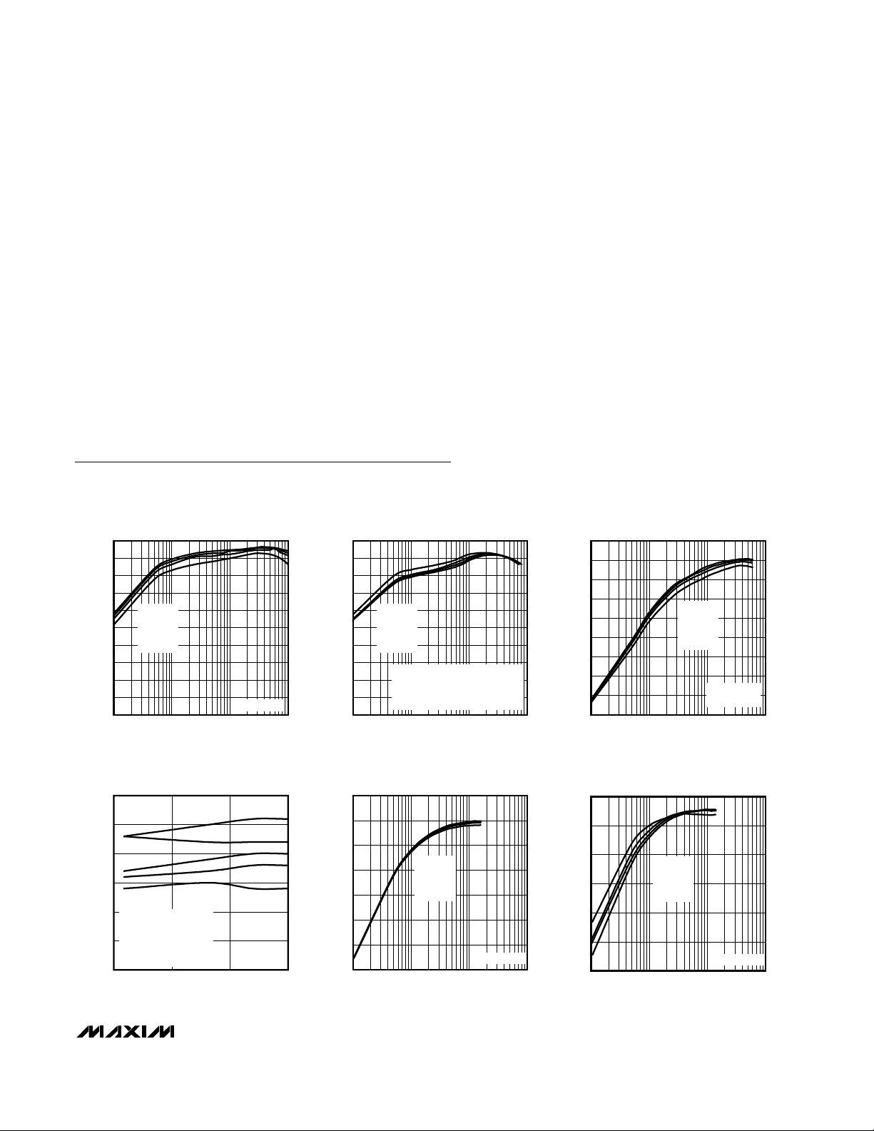
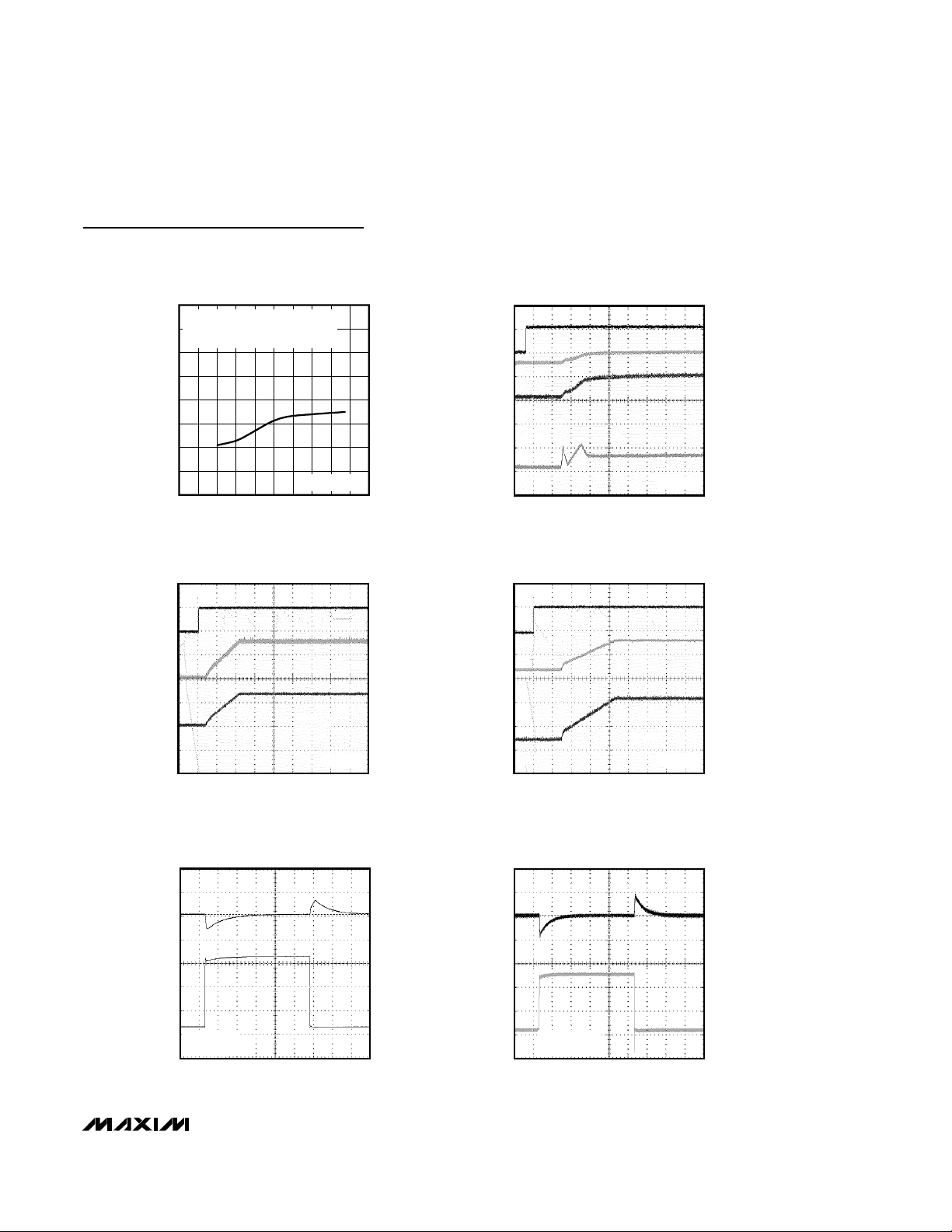
Typical Operating Characteristics
(Circuit of Figure 1, TA= +25°C, unless otherwise noted.)
Note 5: The step-up current limit in startup refers to the LXSU switch current limit, not an output current limit.
Note 6: The idle mode current threshold is the transition point between fixed-frequency PWM operation and idle mode operation
(where switching rate varies with load). The specification is given in terms of inductor current. In terms of output current, the
idle mode transition varies with input-output voltage ratio and inductor value. For the step-up, the transition output current is
approximately 1/3 the inductor current when stepping from 2V to 3.3V. For the step-down, the transition current in terms of
output current is approximately 3/4 the inductor current when stepping down from 3.3V to 1.8V.
Note 7: Operation in dropout (100% duty cycle) can only be maintained for 100,000 OSC cycles before the output is considered
faulted, triggering global shutdown.
Note 8: Specifications to -40°C are guaranteed by design, not production tested.
ELECTRICAL CHARACTERISTICS (continued)
(V
PVSU
= VPV= V
PVSD
= V
INDL2
= 3.6V, TA= -40°C to +85°C, unless otherwise noted.) (Note 8)
STEP-UP EFFICIENCY
vs. LOAD CURRENT
100
90
80
70
60
50
40
EFFICIENCY (%)
30
20
10
VIN = 4.5V
= 4.2V
V
IN
= 3.8V
V
IN
= 3.0V
V
IN
V
= 5V
0
11000
LOAD CURRENT (mA)
OUT
10010
MAX1584/85 toc01
100
90
80
70
60
50
40
EFFICIENCY (%)
30
20
10
0
STEP-DOWN EFFICIENCY
vs. LOAD CURRENT
100
90
80
MAX1584/85 toc02
VIN = 3.0V
= 3.8V
V
IN
= 4.2V
V
IN
= 4.5V
V
IN
PVSD CONNECTED TO BATTERY
= 1.5V
V
OUT
DOES NOT INCLUDE CURRENT USED
BY THE STEP-UP TO POWER THE IC
11000
LOAD CURRENT (mA)
10010
70
60
50
EFFICIENCY (%)
40
30
20
10
COMBINED BOOST-BUCK
EFFICIENCY vs. LOAD CURRENT
VIN = 4.5V
V
IN
V
IN
V
IN
1 1000
LOAD CURRENT (mA)
= 4.2V
= 3.8V
= 3.0V
10010
V
V
OUT3
OUTSU
= 3.3V
= 5.0V
MAX1584/85 toc03
EFFICIENCY vs. INPUT VOLTAGE
100
95
90
85
EFFICIENCY (%)
80
SU = 5V, 300mA
SD = 1.5V, 250mA
SU + AUX3 = 3.3V, 300mA
75
AUX1 = 15V, 40mA
AUX2 = -7.5V, 40mA
70
3.0 4.5
INPUT VOLTAGE (V)
4.03.5
MAX1584/85 toc04
AUX1 EFFICIENCY vs. LOAD CURRENT
MAX1585 AUX2 EFFICIENCY
100
90
80
70
60
EFFICIENCY (%)
50
40
30
11000
VIN = 4.5V
= 4.2V
V
IN
= 3.8V
V
IN
= 3.0V
V
IN
10010
LOAD CURRENT (mA)
V
= 15V
OUT1
MAX5184/85 toc05
90
80
70
60
EFFICIENCY (%)
50
40
30
1 1000
vs. LOAD CURRENT
VIN = 3.0V
= 3.8V
V
IN
= 4.2V
V
IN
= 4.5V
V
IN
10010
LOAD CURRENT (mA)
V
OUT2
MAX5184/85 toc06
= -7.5V
Page 8
MAX1584/MAX1585
5-Channel Slim DSC Power Supplies
8 _______________________________________________________________________________________
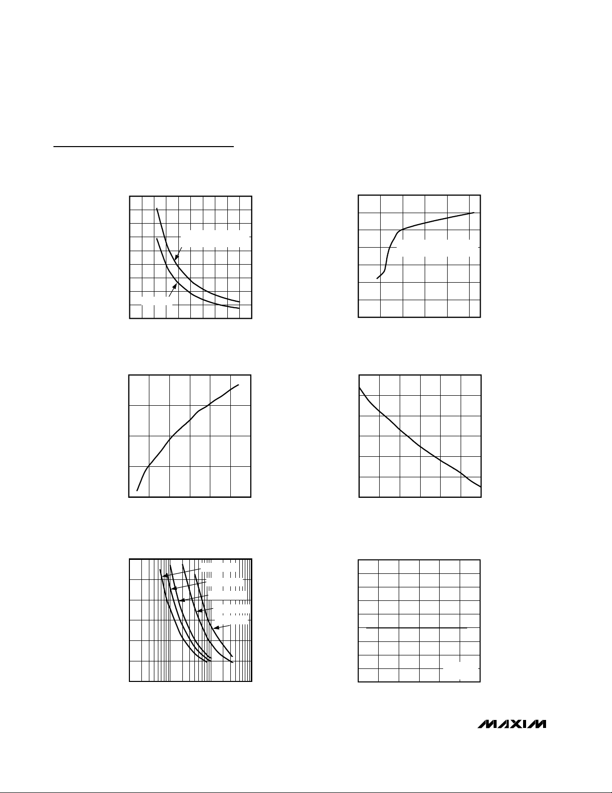
Typical Operating Characteristics (continued)
(Circuit of Figure 1, TA= +25°C, unless otherwise noted.)
NO-LOAD INPUT CURRENT
vs. INPUT VOLTAGE (SWITCHING)
9
8
7
6
5
4
3
INPUT CURRENT (mA)
2
VSU = 5.0V
1
0
05.0
BOOST-BUCK (SU + AUX3)
= 5.0V, OUT3 = 3.33V
V
SU
INPUT VOLTAGE (V)
REFERENCE VOLTAGE
vs. TEMPERATURE
1.254
MAX1584/85 toc07
MINIMUM STARTUP VOLTAGE (V)
4.54.03.0 3.51.0 1.5 2.0 2.50.5
1.250
MINIMUM STARTUP VOLTAGE
vs. LOAD CURRENT (V
3.5
3.0
2.5
2.0
1.5
1.0
0.5
0
0 1000
vs. REFERENCE LOAD CURRENT
SCHOTTKY DIODE CONNECTED
FROM IN TO V
LOAD CURRENT (mA)
SU
800600400200
REFERENCE VOLTAGE
)
SU
MAX5184/85 toc08
1.251
1.248
REFERENCE VOLTAGE (V)
1.246
1.243
-50 100
TEMPERATURE (°C)
OSCILLATOR FREQUENCY vs. R
1100
900
700
500
300
OSCILLATOR FREQUENCY (kHz)
100
-100
11000
C
= 470pF
OSC
C
= 330pF
OSC
C
= 220pF
OSC
C
OSC
C
OSC
10010
R
(kΩ)
OSC
MAX1584/85 toc09
7550250-25
OSC
MAX1584/85 toc11
= 100pF
= 47pF
1.249
1.248
1.247
1.246
REFERENCE VOLTAGE (V)
1.245
1.244
0300
REFERENCE LOAD CURRENT (µA)
MAX1584/85 toc10
25020015010050
SWITCHING FREQUENCY
vs. TEMPERATURE
510
509
508
507
506
505
504
SWITCHING FREQUENCY (kHz)
503
502
501
-50 100
TEMPERATURE (°C)
R
OSC
C
OSC
= 51kΩ
= 100pF
7550250-25
MAX1584/85 toc12
Page 9
MAX1584/MAX1585
5-Channel Slim DSC Power Supplies
_______________________________________________________________________________________ 9
Typical Operating Characteristics (continued)
(Circuit of Figure 1, TA= +25°C, unless otherwise noted.)
MAXIMUM DUTY CYCLE (%)
AUX MAXIMUM DUTY CYCLE
vs. FREQUENCY
88
WHEN THIS DUTY CYCLE IS EXCEEDED
FOR 100,000 CLOCK CYCLES,
87
THE MAX1584/MAX1585 SHUT DOWN
86
85
84
83
82
81
80
0 1000
FREQUENCY (kHz)
STEP-DOWN STARTUP RESPONSE
0V
0V
0A
4ms/div
C
OSC
MAX1584/85 toc15
VIN = 3.5V
= 330pF
900800100 200 300 500 600400 700
MAX1584/85 toc13
ONSD
5V/div
OUTSD
5V/div
I
OUTSD
200mA/div
STEP-UP STARTUP RESPONSE
0V
0V
0A
0A
AUX1 STARTUP RESPONSE
0V
0V
0A
200µs/div
2ms/div
MAX1584/85 toc14
VIN = 3.5V
MAX1584/85 toc16
VIN = 3.5V
ONSU
5V/div
OUTSU
5V/div
I
OUTSU
200mA/div
I
IN
1.0A/div
ON1
5V/div
OUT1
10V/div
I
OUT1
100mA/div
STEP-DOWN LOAD-
STEP-UP LOAD-TRANSIENT RESPONSE
0V
0A
V
= 5.0V
OUTSU
= 3.5V
V
IN
400µs/div
MAX1584/85 toc17
V
OUTSU
AC-COUPLED
500mV/div
I
OUT_SU
200mA/div
0V
0A
TRANSIENT RESPONSE
VIN = 3.5V
= 1.5V
V
OUT_SD
400µs/div
MAX1584/85 toc18
V
OUTSD
AC-COUPLED
100mV/div
I
OUT_SD
100mA/div
Page 10
MAX1584/MAX1585
5-Channel Slim DSC Power Supplies
10 ______________________________________________________________________________________
Pin Description
PIN NAME FUNCTION
AUX1 Controller Compensation Node. Connect a series resistor-capacitor from CC1 to GND to
1 CC1
compensate the converter control loop. This pin is actively driven to GND in shutdown, overload, and
thermal limit. See the AUX Compensation section.
2 FB1
3 PGSD
4 LXSD
AUX1 Controller Feedback Input. The feedback threshold is 1.25V. This pin is high impedance in
shutdown.
Step-Down Power Ground. Connect all PG_ pins together and to GND with short traces as close as
possible to the IC.
Step-Down Converter Switching Node. Connect to the inductor of the step-down converter. LXSD is high
impedance in shutdown.
Step-Down Converter Input. PVSD can connect to PVSU, effectively making OUTSD a boost-buck output
from the battery. Bypass to GND with a 1µF ceramic capacitor if connected to PVSU. PVSD can also be
5 PVSD
6 ONSD
connected to the battery but should not exceed PVSU by more than a Schottky diode forward voltage.
Bypass PVSD with a 10µF ceramic capacitor when connecting to the battery input. A 10kΩ internal
resistance connects PVSU and PVSD.
Step-Down Converter On/Off Control Input. Logic high = on; however, turn-on is locked out until the step-
up has reached regulation. This pin has an internal 330kΩ pulldown resistance to GND.
Step-Up Converter Compensation Node. Connect a series resistor-capacitor from CCSD to GND to
7 CCSD
8 FBSD
9 ON1
10 ON2
11 ON3
compensate the converter control loop. This pin is actively driven to GND in shutdown, overload, and
thermal limit. See the Step-Down Compensation section.
Step-Down Converter Feedback Input. Connect a resistive voltage-divider from OUTSD to FBSD to GND.
The FBSD feedback threshold is 1.25V. This pin is high impedance in shutdown.
AUX1 Controller On/Off Input. Logic high = on; however, turn-on is locked out until 1024 OSC cycles after
the step-up has reached regulation. This pin has an internal 330kΩ pulldown resistance to GND.
AUX2 Controller On/Off Input. Logic high = on; however, turn-on is locked out until 1024 OSC cycles after
the step-up has reached regulation. This pin has an internal 330kΩ pulldown resistance to GND.
AUX3 Controller On/Off Input. Logic high = on; however, turn-on is locked out until 1024 OSC cycles after
the step-up has reached regulation. This pin has an internal 330kΩ pulldown resistance to GND.
Step-Up Converter On/Off Control. Logic high = on. All other ON_ pins are locked out until 1024 OSC
12 ONSU
cycles after the step-up DC-DC converter output has reached its final value. This pin has an internal
330kΩ pulldown resistance to GND.
13 REF
14 FBSU
Reference Output. Bypass REF to GND with a 0.1µF or greater capacitor. The maximum allowed load on
REF is 200µA. REF is actively pulled to GND when all converters are shut down.
Step-Up Converter Feedback Input. Connect a resistive voltage-divider from PVSU to FBSU to GND. The
FBSU feedback threshold is 1.25V. This pin is high impedance in shutdown.
Step-Up Converter Compensation Node. Connect a series resistor-capacitor from CCSU to GND to
15 CCSU
compensate the converter control loop. This pin is actively driven to GND in shutdown, overload, and
thermal limit. See the Step-Up Compensation section.
Page 11

MAX1584/MAX1585
5-Channel Slim DSC Power Supplies
______________________________________________________________________________________ 11
Pin Description (continued)
PIN NAME FUNCTION
16 AUX1OK
17 SDOK
Open-Drain Power-OK Signal for AUX1 Controller. AUX1OK is low when the AUX1 controller has
successfully completed soft-start. This pin is high impedance in shutdown, overload, and thermal limit.
Open-Drain Power-OK Signal for Step-Down Converter. SDOK is low when the step-down has successfully
completed soft-start. This pin is high impedance in shutdown, overload, and thermal limit.
Short-Circuit Flag, Active-Low, Open-Drain Output. SCF is high impedance when overload protection
18 SCF
occurs and during startup. SCF can drive high-side PFET switches connected to one or more outputs to
completely disconnect the load when the channel turns off in response to a logic command or an
overload. See the Status Outputs (
SDOK, AUX1OK
, SCF) section.
Oscillator Control. Connect a timing capacitor from OSC to GND and a timing resistor from OSC to PVSU
19 OSC
20 PGSU
21 LXSU
22 PVSU
(or other DC voltage) to set the oscillator frequency between 100kHz and 1MHz. See the Setting the
Switching Frequency section. This pin is high impedance in shutdown.
Step-Up Power Ground. Connect all PG_ pins together and to GND with short traces as close to the IC as
possible.
Step-Up Converter Switching Node. Connect to the inductor of the step-up converter. LXSU is high
impedance in shutdown.
Power Output of the Step-Up DC-DC Converter. Connect the output filter capacitor from PVSU to PGSU.
PVSU can also power other converter channels. Connect PVSU to PV at the IC.
MAX1585 (AUX2 inverter): The FB2 feedback threshold is 0V.
Connect a resistive voltage-divider from the output voltage to FB2 to
REF to set the output voltage.
MAX1584 (AUX2 step-up): The FB2 feedback threshold is 1.25V.
Connect a resistive voltage-divider from the output voltage to FB2 to
GND to set the output voltage.
23 FB2
AUX2 Controller Feedback Input.
This pin is high impedance in
shutdown.
AUX2 Controller Compensation Node. Connect a series resistor-capacitor from CC2 to GND to
24 CC2
compensate the control loop. CC2 is actively driven to GND in shutdown and thermal limit. See the AUX
Compensation section.
MAX1585 (AUX2 inverter): Connect INDL2 to the external P channel
MOSFET source (typically the battery) to ensure the P channel is
completely off when D2 swings high.
MAX1584 (AUX2 step-up): Connect INDL2 to PVSU for optimum
N-channel gate drive.
25 INDL2
Voltage Input for the AUX2 Gate
Driver. The voltage at INDL2 sets
the high gate-drive voltage.
26 PV IC Power Input. Connect PVSU and PV together.
MAX1585: DL2 drives a PFET in an inverter configuration. In
shutdown, overload, and thermal limit, DL2 is driven high.
MAX1584: DL2 drives an N-channel FET in a boost/flyback
configuration. In shutdown, overload, and thermal limit, DL2 is driven
low.
27 DL2
AUX2 Controller Gate-Drive
Output. DL2 drives between
INDL2 and GND.
Page 12

MAX1584/MAX1585
5-Channel Slim DSC Power Supplies
12 ______________________________________________________________________________________
Detailed Description
The MAX1584/MAX1585 are complete power-conversion ICs for slim digital still cameras. They can accept
input from a variety of sources, including single-cell Li+
batteries and 2-cell alkaline or NiMH batteries, as well
as systems designed to accept both battery types. The
MAX1584/MAX1585 include five DC-DC converter
channels to generate all required voltages (Figure 2
shows a functional diagram):
• Synchronous-rectified step-up DC-DC converter with
on-chip MOSFETs—Typically supplies 3.3V for main
system power or 5V to power other DC-DC converters for boost-buck designs.
• Synchronous-rectified step-down DC-DC converter
with on-chip MOSFETs—Typically supplies 1.8V for
the DSP core. Powering the step-down from the
step-up output provides efficient (up to 90%) boostbuck functionality that supplies a regulated output
when the battery voltage is above or below the output voltage. The step-down can also be powered
from the battery if there is sufficient headroom.
• AUX1 step-up controller—Typically used for 15V to
bias one or more of the LCD, CCD, and LED backlights.
• AUX2 step-up controller (MAX1584)—Typically supplies remaining bias voltages with either a multi-output flyback transformer or a boost converter with
charge-pump inverter. Alternately, can power white
LEDs for LCD backlighting.
• AUX2 inverter controller (MAX1585)—Typically supplies negative CCD bias when high current is needed for large pixel-count CCDs.
• AUX3 step-down controller—Typically steps 5V generated at PVSU down to 3.3V for system logic in
boost-buck designs.
Step-Up DC-DC Converter
The step-up DC-DC switching converter is typically used
to generate a 5V output voltage from a 1.5V to 4.5V battery input, but any voltage from VINto 5V can be set. An
internal NFET switch and a PFET synchronous rectifier
allow conversion efficiencies as high as 95%. Under
moderate to heavy loading, the converter operates in a
low-noise PWM mode with constant frequency and modulated pulse width. Switching harmonics generated by
fixed-frequency operation are consistent and easily filtered. Efficiency is enhanced under light (<75mA typ)
loading, by an idle mode that switches the step-up only
as needed to service the load. In this mode, the maximum inductor current is 250mA for each pulse.
Pin Description (continued)
PIN NAME FUNCTION
28 DL3
29 DL1
AUX3 Step-Down Controller Gate-Drive Output. Connect to the gate of a P-channel MOSFET. DL3 swings
from GND to PVSU and supplies up to 500mA. DL3 is driven to PVSU in shutdown and thermal limit.
AUX1 Step-Up Controller Gate-Drive Output. Connect to the gate of an N-channel MOSFET. DL1 swings
from GND to PVSU and supplies up to 500mA. DL1 is driven to GND in shutdown and thermal limit.
30 GND Analog Ground. Connect to all PG_ pins as close to the IC as possible.
AUX3 Step-Down Controller Compensation Node. Connect a series resistor-capacitor from CC3 to FB3 to
31 CC3
compensate the converter control loop. This pin is actively driven to GND in shutdown, overload, and
thermal limit. See the AUX Compensation section.
PWM Step-Up Controller 3 Feedback Input. Connect a resistive voltage-divider from the output voltage to
32 FB3
FB3 to GND to set the output voltage. The FB3 feedback threshold is 1.25V. This pin is high impedance in
shutdown.
Exposed Underside Metal Pad. This pad must be soldered to the PC board to achieve package thermal
PAD EP
and mechanical ratings. There is no internal metal or bond wire physically connecting the exposed pad to
the GND pin(s). Connecting the exposed pad to ground does not remove the requirement for a good
ground connection to the appropriate IC pins.
Page 13

MAX1584/MAX1585
5-Channel Slim DSC Power Supplies
______________________________________________________________________________________ 13
Figure 1. MAX1584/MAX1585 Typical Application for 2-Cell AA or 1-Cell Li+ Battery
47k
0.01µF
C1
R1
Ω
25k
4700pF
C2
R2
Ω
-7.5V
-CDD
BIAS
526k
93.1k
20k
1500pF
1.5V TO 4.2V
R8
Ω
R9
Ω
R3
Ω
10k
C3
1500pF
V
IN
10µF
C8
4.7µF
TO PVSU
R5
Ω
C5
C24
D2
61.9k
470pF
0.1µF
20k
330pF
R4
Ω
C4
P1
L6
3.6µH
Ω
TO FB3
INDL2
DL2
FB2
REF
1.25V
OSC
CCSU
CCSD
CC1
CC2
CC3
ONSU
ONSD
ON1
ON2
ON3
AUX1OK
REF
MAX1585
AUX2
V-MODE
INV
PWM
CURRENT-
MODE
STEP-UP
CURRENT-
MODE
STEPDOWN
AUX1
V-MODE
STEP-UP
PWM
AUX3 V-MODE
STEP-DOWN
PWM
DL1
FB1
DL3
FB3
PVSU
LXSU
PGSU
FBSU
PVSD
LXSD
PGSD
FBSD
L3
2µH
N1
P2
D3
L1
5µH
C19
10µF
D4
OR PVSU
TO V
IN
L2
22µH
30µF
PV
C9
D1
10µH
TO V
L4
C23
10µF
C25
47µF
IN
C11
47µF
C6
4.7µF
TO PVSU
OR V
R10
18.2k
IN
R15
18.2k
R12
274k
R13
90.9k
R6
1M
Ω
R14
30.1k
Ω
5V 1A
MAIN SYSTEM
Ω
Ω
+1.5V
250mA
CORE
Ω
+15V, 80mA
+CCD
LCD
LED
R7
90.9k
Ω
C20
560pF
Ω
3.3V
250mA
LOGIC
R22
1.2k
Ω
SCF
SDOK
GND
R11
90.9k
Ω
Page 14

MAX1584/MAX1585
5-Channel Slim DSC Power Supplies
14 ______________________________________________________________________________________
Figure 2. MAX1584/MAX1585 Functional Diagram
PVSU
2.35V
ONSU
V
ONSU
OSC
REF
1V
INTERNAL
POWER-OK
REFOK
REF
CCSU
FBSU
STEP-UP
SOFT-START
DONE (SUSSD)
CCSD
SOFT-START
RAMP
GENERATOR
100,000
CLOCK CYCLE
FAULT TIMER
150ns
ONE-SHOT
TO
V
NORMAL
MODE
OVER
TEMP
FAULT
IN
CLK
REF
FLTALL
FAULT
CURRENT-MODE
STEP-UP
FAULT
DC-DC
STARTUP
OSCILLATOR
TO INTERNAL
POWER
1.25V
REFERENCE
FLTALL
MAX1584/
MAX1585
SCF
PV
REF
GND
PVSU
LXSU
PGSU
ONSU
PVSD
FBSD
ONSD
SOFT-START
RAMP GENERATOR
SUSSD
FLTALL
CURRENT-MODE
DC-DC
STEP-DOWN
TO
V
REF
TO AUX_
CHANNELS
(SEE FIGURE 3)
LXSD
PGSD
SDOK
Page 15

MAX1584/MAX1585
5-Channel Slim DSC Power Supplies
______________________________________________________________________________________ 15
Step-Down DC-DC Converter
The step-down DC-DC converter is optimized for generating low output voltages (down to 1.25V) at high efficiency. Output voltages lower than 1V can be set by
adding an additional resistor (see the Applications
Information section). The step-down runs from the voltage at PVSD. This pin can be connected directly to the
battery if sufficient headroom exists to avoid dropout;
otherwise, PVSD can be powered from the output of
another converter. The step-down can also operate
with the step-up for boost-buck operation.
Under moderate to heavy loading, the converter operates in a low-noise PWM mode with constant frequency
and modulated pulse width. Efficiency is enhanced
under light (<75mA typ) loading by assuming an idle
mode during which the step-down switches only as
needed to service the load. In this mode, the maximum
inductor current is 100mA for each pulse. The stepdown DC-DC is inactive until the step-up DC-DC is in
regulation.
The step-down also features an open-drain SDOK out-
put that goes low when the step-down output is in regulation. SDOK can be used to drive an external MOSFET
switch that gates 3.3V power to the processor after the
core voltage is in regulation. This connection is shown
in Figure 13.
Boost-Buck Operation
The step-down input can be powered from the output
of the step-up. By cascading these two channels, the
step-down output can maintain regulation even as the
battery voltage falls below the step-down output voltage. This is especially useful when trying to generate
3.3V from 1-cell Li+ inputs, or 2.5V from 2-cell alkaline
or NiMH inputs, or when designing a power supply that
must operate from both Li+ and alkaline/NiMH inputs.
Compound efficiencies of up to 90% can be achieved
when the step-up and step-down are operated in
series.
Note that the step-up output supplies both the step-up
load and the step-down input current when the stepdown is powered from the step-up. The step-down
input current reduces the available step-up output current for other loads.
Direct Battery Step-Down Operation
The step-down converter can also be operated directly
from the battery as long as the voltage at PVSD does
not exceed PVSU by more than a Schottky diode forward voltage. When using this connection, connect an
external Schottky diode from the battery input to PVSU.
On the MAX1584/MAX1585, there is an internal 10kΩ
resistance from PVSU to PVSD. This adds a small addi-
tional current drain (of approximately (V
PVSU
- V
PVSD
) /
10kΩ) from PVSU when PVSD is not connected directly
to PVSU.
Step-down direct battery operation improves efficiency
for the step-down output (up to 95%), but restricts the
upper limit of the output voltage to 200mV less than the
minimum battery voltage. In 1-cell Li+ designs (with a
2.7V min), the output can be set up to 2.5V. In 2-cell
alkaline or NiMH designs, the output can be limited to
1.5V or 1.8V, depending on the minimum-allowed cell
voltage.
The step-down can only be briefly operated in dropout
since the MAX1584/MAX1585 fault protection detects
the out-of-regulation condition and activates after
100,000 OSC cycles (200ms at f
OSC
= 500kHz). At that
point, all MAX1584/MAX1585 channels shut down.
AUX1, AUX2, and AUX3 DC-DC Controllers
The three auxiliary controllers operate as fixed-frequency voltage-mode PWM controllers. They do not have
internal MOSFETs, so output power is determined by
external components. The controllers regulate output
voltage by modulating the pulse width of the DL_ drive
signal to an external MOSFET switch. The MAX1584
contains two step-up/flyback controllers (AUX1 and
AUX2) and one step-down controller (AUX3). The
MAX1585 contains one step-up controller (AUX1), one
inverting controller (AUX2), and one step-down controller (AUX3).
Figure 3 shows a functional diagram of the AUX controllers. The inverting and step-down controllers differ
from the step-up controllers only in the gate-drive logic
and FB polarity and threshold. The sawtooth oscillator
signal at OSC governs timing. At the start of each
cycle, DL_ turns on the external MOSFET switch. For
step-up controllers, DL_ goes high, while for inverting
and step-down controllers, DL_ goes low (to turn on
PFETs). The external MOSFET then turns off when the
internally level-shifted sawtooth rises above CC_ or
when the maximum duty cycle is exceeded. The switch
remains off until the start of the next cycle. A transconductance error amplifier forms an integrator at CC_ so
that high DC loop gain and accuracy can be maintained. In step-up and step-down controllers, the FB_
threshold is 1.25V, and higher FB_ voltages reduce the
MOSFET duty cycle. In inverting controllers, the FB_
threshold is 0V, and lower (more negative) FB_ voltages reduce the MOSFET duty cycle.
Auxiliary controllers do not start until the step-up DC-DC
output is in regulation. If the step-up, step-down, or any
of the auxiliary controllers remains faulted for 100,000
Page 16

MAX1584/MAX1585
5-Channel Slim DSC Power Supplies
16 ______________________________________________________________________________________
OSC cycles, then all MAX1584/MAX1585 channels latch
off.
Maximum Duty Cycle
The MAX1584/MAX1585 auxiliary PWM controllers have
a guaranteed maximum duty cycle of 80%. In boost
designs that employ continuous current, the maximum
duty cycle limits the boost ratio so that:
1 - VIN/ V
OUT
≤ 80%
With discontinuous inductor current, no such limit exists
for the input/output ratio since the inductor has time to
fully discharge before the next cycle begins.
AUX1
AUX1 can be used for conventional DC-DC boost and
flyback designs (Figure 5). Its output (DL1) is designed
Figure 3. AUX Controller Functional Diagrams
FB_
CC_
LEVEL
SHIFT
0.85
REF
REFI
(REFI RAMPS FROM
0V TO REF IN 1024 OSC
REF
OSC
MAX1584 AUX1 AND
AUX2, MAX1585 AUX1
STEP-UP CONTROLLER
SOFT-START
CYCLES)
CLK
R
S
FAULT
PROTECTION
FB3
CC3
REF
Q
ENABLE
0.85
REF
REFI
0V TO REF IN 1024 OSC
FB2
CC2
DL_
REF
OSC
MAX1584 AND MAX1585
LEVEL
SHIFT
SOFT-START
(REFI RAMPS FROM
CYCLES)
REFI
0.85
REF
AUX3 STEP-DOWN
CONTROLLER
R
S
LEVEL
SHIFT
SOFT-START
(REFI RAMPS FROM
REF TO 0V IN 1024 OSC
CYCLES)
Q
MAX1585 AUX2
INVERTING CONTROLLER
R
S
CLK
FAULT
PROTECTION
DL3
Q
DL2
ENABLE
CLK
OSC
FAULT
PROTECTION
ENABLE
Page 17

MAX1584/MAX1585
5-Channel Slim DSC Power Supplies
______________________________________________________________________________________ 17
to drive an N-channel MOSFET. Its feedback (FB1)
threshold is 1.25V.
AUX2
In the MAX1584, AUX2 is identical to AUX1.
In the MAX1585, AUX2 is an inverting controller that
generates a regulated negative output voltage, typically
for CCD and LCD bias. This is handy in height-limited
designs where transformers might not be desired.
The AUX2 MOSFET driver (DL2) in the MAX1585 is
designed to drive P-channel MOSFETs. DL2 swings
from GND to PVSU. See Figure 8 for a typical inverter
configuration.
AUX3 DC-DC Step-Down Controller
AUX3 can be used for conventional DC-DC step-down
(buck) designs (Figure 1). Its output (DL3) is designed to
drive a P-channel MOSFET and swings from GND to
PVSU. Its feedback (FB3) threshold is 1.25V.
Master/Slave Configurations
The MAX1584/MAX1585 support the MAX1801 slave
PWM controllers that obtain input power, a voltage reference, and an oscillator signal directly from the
MAX1584/MAX1585 master. The master/slave configuration allows channels to be easily added and minimizes system cost by eliminating redundant circuitry.
The slaves also control the harmonic content of noise
since their operating frequency is synchronized to that
of the MAX1584/MAX1585 master converter. A
MAX1801 connection to the MAX1584/MAX1585 is
shown in Figure 12.
Status Outputs (
SDOK, AUX1OK
, SCF)
The MAX1584/MAX1585 include three versatile status
outputs that can provide information to the system. All
are open-drain outputs and can directly drive MOSFET
switches to facilitate sequencing, disconnect loads
during overloads, or perform other hardware-based
functions.
SDOK pulls low when the step-down has successfully
completed soft-start. SDOK goes high impedance in
shutdown, overload, and thermal limit. A typical use for
SDOK is to enable 3.3V power to the CPU I/O after the
CPU core is powered up (Figure 13), thus providing safe
sequencing in hardware without system intervention.
AUX1OK pulls low when the AUX1 controller has successfully completed soft-start. AUX1OK goes high
impedance in shutdown, overload, and thermal limit. A
typical use for AUX1OK is to drive a P-channel MOSFET
that gates 5V power to the CCD until the +15V CCD bias
(generated by AUX1) is powered up (Figure 14).
SCF goes high (high impedance, open drain) when
overload protection occurs. Under normal operation,
SCF pulls low. SCF can drive a high-side P-channel
MOSFET switch that can disconnect a load during
power-up or when a channel turns off in response to a
logic command or an overload. Several connections
are possible for SCF. One is shown in Figure 15, where
SCF provides load disconnect for the step-up on fault
and power-up.
Soft-Start
The MAX1584/MAX1585 channels feature a soft-start
function that limits inrush current and prevents excessive battery loading at startup by ramping the output
voltage of each channel up to the regulation voltage.
This is accomplished by ramping the internal reference
inputs to each channel error amplifier from 0V to the
1.25V reference voltage over a period of 4096 oscillator
cycles (16ms at 500kHz) when initial power is applied
or when a channel is enabled. Soft-start is not included
in the step-up converter in order to avoid limiting startup capability with loading.
The step-down soft-start ramp takes half the time (2048
clock cycles) of the other channel ramps. This allows
the step-down and AUX3 output (when set to 3.3V) to
track each other and rise at nearly the same dV/dt rate
on power-up. Once the step-down output reaches its
regulation point (1.5V or 1.8V typ), the AUX3 output
(3.3V typ) continues to rise at the same ramp rate.
Fault Protection
The MAX1584/MAX1585 have robust fault and overload
protection. After power-up, the device is set to detect
an out-of-regulation state that could be caused by an
overload or short. If any DC-DC converter channel
(step-up, step-down, or any of the auxiliary controllers)
remains faulted for 100,000 clock cycles (200ms at
500kHz), then all outputs latch off until the step-up DCDC converter is reinitialized by the ONSU pin or by
cycling the input power. The fault-detection circuitry for
any channel is disabled during its initial turn-on softstart sequence.
An exception to the standard fault behavior is that there
is no 100,000 clock-cycle delay in entering the fault
state if the step-up output (PVSU) is dragged below its
2.5V UVLO threshold or is shorted. The step-up UVLO
immediately triggers and shuts down all channels. The
step-up then continues to attempt to start. If the step-up
output short remains, these attempts do not succeed
since PVSU remains near ground.
If a soft-short or overload remains on PVSU, the startup
oscillator switches the internal N-channel MOSFET, but
fault is retriggered if regulation is not achieved by the
Page 18

MAX1584/MAX1585
end of the soft-start interval. If PVSU is dragged below
the input, the overload is supplied by the body diode of
the internal synchronous rectifier or by a Schottky diode
connected from the battery to PVSU. If desired, this
overload current can be interrupted by a P-channel
MOSFET controlled by SCF, as shown in Figure 15.
Reference
The MAX1584/MAX1585 have internal 1.250V references. Connect a 0.1µF ceramic bypass capacitor from
REF to GND within 0.2in (5mm) of the REF pin. REF can
source up to 200µA and is enabled when ONSU is high
and PVSU is above 2.5V. The auxiliary controllers and
MAX1801 slave controllers (if connected) each sink up
to 30µA REF current during startup. If the application
requires that REF be loaded beyond 200µA, buffer REF
with a unity-gain amplifier or op amp.
Oscillator
All MAX1584/MAX1585 DC-DC converter channels
employ fixed-frequency PWM operation. The operating
frequency is set by an RC network at the OSC pin. The
range of usable settings is 100kHz to 1MHz. When
MAX1801 slave controllers are added, they operate at
the frequency set by OSC.
The oscillator uses a comparator, a 150ns one-shot,
and an internal NFET switch in conjunction with an
external timing resistor and capacitor (Figure 4). When
the switch is open, the capacitor voltage exponentially
approaches the step-up output voltage from zero with a
time constant given by the product of R
OSC
and C
OSC
.
The comparator output switches high when the capacitor voltage reaches V
REF
(1.25V). In turn, the one-shot
activates the internal MOSFET switch to discharge the
capacitor within a 150ns interval, and the cycle
repeats. The oscillation frequency changes as the main
output voltage ramps upward following startup. The
oscillation frequency is then constant once the main
output is in regulation.
Low-Voltage Startup Oscillator
The MAX1584/MAX1585 internal control and referencevoltage circuitry receive power from PVSU and do not
function when PVSU is less than 2.5V. To ensure lowvoltage startup, the step-up employs a low-voltage
startup oscillator that activates at 0.9V if a Schottky rectifier is connected from V
BATT
to PVSU (1.1V with no
Schottky rectifier). The startup oscillator drives the internal N-channel MOSFET at LXSU until PVSU reaches
2.5V, at which point voltage control is passed to the
current-mode PWM circuitry.
Once in regulation, the MAX1584/MAX1585 operate
with inputs as low as 0.7V since internal power for the
IC is supplied by PVSU. At low input voltages, the stepup can have difficulty starting into heavy loads (see the
Minimum Startup Voltage vs. Load Current graph in the
Typical Operating Characteristics section); however,
this can be remedied by connecting an external Pchannel load switch driven by SCF so the load is not
connected until the PVSU is in regulation (Figure 15).
ON_ Control Inputs
The step-up converter activates with a high input at
ONSU. The step-down and auxiliary DC-DC converters
1, 2, and 3 activate with a high input at ONSD, ON1,
ON2, and ON3, respectively. The step-down and auxil-
5-Channel Slim DSC Power Supplies
18 ______________________________________________________________________________________
Figure 4. Oscillator Functional Diagram
Figure 5. +15V LCD Bias with Basic Boost Topology
V
OSC
SU
R
OSC
C
OSC
V
REF
(1.25V)
150ns
ONE-SHOT
MAX1584
MAX1585
(PARTIAL)
AUX
PWM
PVSU
DL_
TO
V
BATT
+15V
Q1
D6
50mA
LCD
MAX1584
MAX1585
FB_
NOTE: THIS CIRCUIT CAN OPERATE WITH AUX1 OR
AUX2 ON THE MAX1584, AND WITH AUX1 ON THE MAX1585
Page 19

iary converters and cannot be activated until PVSU is in
regulation. For automatic startup, connect ON_ to PVSU
or a logic level greater than 1.6V.
Design Procedure
Setting the Switching Frequency
Choose a switching frequency to optimize external
component size or circuit efficiency for the particular
application. Typically, switching frequencies between
400kHz and 500kHz offer a good balance between
component size and circuit efficiency—higher frequencies generally allow smaller components, and lower frequencies give better conversion efficiency. The
switching frequency is set with an external timing resistor
(R
OSC
) and capacitor (C
OSC
). At the beginning of a
cycle, the timing capacitor charges through the resistor
until it reaches V
REF
. The charge time, t1, is as follows:
t1 = -R
OSC
x C
OSC
x ln(1 - 1.25 / V
PVSU
)
The capacitor voltage then decays to zero over time t
2
= 150ns. The oscillator frequency is as follows:
f
OSC
= 1 / (t1+ t2)
f
OSC
can be set from 100kHz to 1MHz. Choose C
OSC
between 22pF and 470pF. Determine R
OSC
:
R
OSC
= (150ns - 1 / f
OSC
) / (C
OSC
x ln[1 - 1.25
V
PVSU
])
See the Typical Operating Characteristics section for
f
OSC
vs. R
OSC
using different values of C
OSC
.
Setting Output Voltages
The MAX1584/MAX1585 step-up and step-down converters and the AUX1 controllers have resistoradjustable output voltages. When setting the voltage for
all channels except AUX2 on the MAX1585, connect a
resistive voltage-divider from the output voltage to the
corresponding FB_ input. The FB_ input bias current is
less than 100nA, so choose the low-side (FB_-to-GND)
resistor (RL) to be 100kΩ or less. Then calculate the
high-side (output-to-FB_) resistor (RH):
RH= RL[(V
OUT
/ 1.25) - 1]
AUX2 is an inverter on the MAX1585, so the FB2
threshold on the MAX1585 is 0V. To set the MAX1585
AUX2 negative output voltage, connect a resistive voltage-divider from the negative output to the FB2 input,
and then to REF. The FB2 input bias current is less than
100nA, so choose the REF-side (FB2-to-REF) resistor
(R
REF
) to be 100kΩ or less. Then calculate the top-side
(negative output-to-FB2) resistor:
R
TOP
= R
REF
(-V
OUT(AUX2)
/ 1.25)
General Filter-Capacitor Selection
The input capacitor in a DC-DC converter reduces current peaks drawn from the battery or other input power
source and reduces switching noise in the controller.
The impedance of the input capacitor at the switching
frequency should be less than that of the input source
so high-frequency switching currents do not pass
through the input source.
The output capacitor keeps output ripple small and
ensures control-loop stability. The output capacitor
must also have low impedance at the switching frequency. Ceramic, polymer, and tantalum capacitors
are suitable, with ceramic exhibiting the lowest ESR
and high-frequency impedance.
Output ripple with a ceramic output capacitor is
approximately:
V
RIPPLE
= I
L(PEAK)
[1 / (2π x f
OSC
x C
OUT
)]
If the capacitor has significant ESR, the output ripple
component due to capacitor ESR is:
V
RIPPLE(ESR)
= I
L(PEAK)
x ESR
Output capacitor specifics are also discussed in each
converter’s Compensation section.
Step-Up Component Selection
The external components required for the step-up are
an inductor, an input and output filter capacitor, and a
compensation RC.
The inductor is typically selected to operate with continuous current for best efficiency. An exception might be
if the step-up ratio, (V
OUT
/ VIN), is greater than 1 / (1 -
D
MAX
), where D
MAX
is the maximum PWM duty factor
of 80%.
When using the step-up channel to boost from a low
input voltage, loaded startup is aided by connecting a
Schottky diode from the battery to PVSU. See the
Minimum Startup Voltage vs. Load Current graph in the
Typical Operating Characteristics section.
Step-Up Inductor
In most step-up designs, a reasonable inductor value
(L
IDEAL
) can be derived from the following equation,
which sets continuous peak-to-peak inductor current at
half the DC inductor current:
L
IDEAL
= [2V
IN(MAX)
x D(1 - D)] / (I
OUT
x f
OSC
)
where D is the duty factor given by:
D = 1 - (V
IN
/ V
OUT
)
Given L
IDEAL
, the consistent peak-to-peak inductor cur-
rent is 0.5 x I
OUT
/ (1 - D). The peak inductor current is
as follows:
MAX1584/MAX1585
5-Channel Slim DSC Power Supplies
______________________________________________________________________________________ 19
Page 20

MAX1584/MAX1585
I
IND(PK)
= 1.25 x I
OUT
/ (1 - D)
Inductance values smaller than L
IDEAL
can be used to
reduce inductor size; however, if much smaller values are
used, inductor current rises and a larger output capacitance might be required to suppress output ripple.
Step-Up Compensation
The inductor and output capacitor are usually chosen
first in consideration of performance, size, and cost.
The compensation resistor and capacitor are then chosen to optimize control-loop stability. In some cases, it
helps to readjust the inductor or output capacitor value
to get optimum results. For typical designs, the component values in the circuit of Figure 1 yield good results.
The step-up converter employs current-mode control,
thereby simplifying the control-loop compensation.
When the converter operates with continuous inductor
current (typically the case), a right-half-plane zero
appears in the loop-gain frequency response. To
ensure stability, the control-loop gain should cross over
(drop below unity gain) at a frequency (fC) much less
than that of the right-half-plane zero.
The relevant characteristics for step-up channel compensation are as follows:
• Transconductance (from FBSU to CCSU), g
MEA
(135µS)
• Current-sense amplifier transresistance, R
CS
(0.3V/A)
• Feedback regulation voltage, VFB(1.25V)
• Step-up output voltage, VSU, in V
• Output load equivalent resistance, R
LOAD
, in
Ω = V
SUOUT
/ I
LOAD
The key steps for step-up compensation are as follows:
1) Place fCsufficiently below the right-half-plane zero
(RHPZ) and calculate CC.
2) Select RCbased on the allowed load-step transient.
RCsets a voltage delta on the CCpin that corresponds to load-current step.
3) Calculate the output-filter capacitor (C
OUT
) required
to allow the RCand CCselected.
4) Determine if CPis required (if calculated to be >10pF).
For continuous conduction, the right-half-plane zero frequency (f
RHPZ
) is given by the following:
f
RHPZ
= V
SUOUT
(1 - D)2 / (2π x L x I
LOAD
)
where D = the duty cycle = 1 - (V
IN
/ V
OUT
), L is the
inductor value, and I
LOAD
is the maximum output current. Typically, target crossover (fC) for 1/6 of the
RHPZ. For example, if we assume f
OSC
= 500kHz, V
IN
= 2.5V, V
OUT
= 5V, and I
OUT
= 0.5A, then R
LOAD
=
10Ω. If we select L = 4.7µH, then:
f
RHPZ
= 5 (2.5 / 5)2 / (2π x 4.7 x 10-6x 0.5) = 84.65kHz
Choose fC= 14kHz. Calculate CC:
CC= (V
FB
/ V
OUT
)(R
LOAD
/ RCS)(gM/ 2π x fC)(1 - D)
= (1.25 / 5)(10 / 0.3) x (135µS / (6.28 x 14kHz) (2/5)
= 6.4nF
Choose 6.8nF.
Now select RCso transient-droop requirements are
met. As an example, if 4% transient droop is allowed,
the input to the error amplifier moves 0.04 x 1.25V, or
50mV. The error-amp output drives 50mV x 135µS, or
6.75µA across RCto provide transient gain. Since the
current-sense transresistance is 0.3V/A, the value of R
C
that allows the required load step swing is as follows:
RC= 0.3 I
IND(PK)
/ 6.75µA
In a step-up DC-DC converter, if L
IDEAL
is used, output
current relates to inductor current by:
I
IND(PK)
= 1.25 x I
OUT
/ (1 - D) = 1.25 x I
OUT
x V
OUT
/
V
IN
So for a 500mA output load step with VIN= 2.5V and
V
OUT
= 5V:
RC= [1.25(0.3 x 0.5 x 5) / 2)] / 6.75µA = 69.4kΩ
Note that the inductor does not limit the response in this
case since it can ramp at 2.5V / 4.7µH, or 530mA/µs.
The output filter capacitor is then chosen so the C
OUT
R
LOAD
pole cancels the RCCCzero:
C
OUT
x R
LOAD
= RCx C
C
For the example:
C
OUT
= 68kΩ x 6.8nF / 10Ω = 46µF
Choose 47µF for C
OUT
. If the available C
OUT
is substantially different from the calculated value, insert the
available C
OUT
value into the above equation and
recalculate RC. Higher substituted C
OUT
values allow a
higher RC, which provides higher transient gain and
consequently less transient droop.
If the output filter capacitor has significant ESR, a zero
occurs at the following:
Z
ESR
= 1 / (2π x C
OUT
x R
ESR
)
5-Channel Slim DSC Power Supplies
20 ______________________________________________________________________________________
Page 21

If Z
ESR
> fC, it can be ignored, as is typically the case
with ceramic output capacitors. If Z
ESR
is less than fC,
it should be cancelled with a pole set by capacitor C
P
connected from CCSU to GND:
CP= C
OUT
x R
ESR
/ R
C
If CPis calculated to be <10pF, it can be omitted.
Step-Down Component Selection
Step-Down Inductor
The external components required for the step-down
are an inductor, input and output filter capacitors, and
a compensation RC network.
The MAX1585/1585 step-down converter provides best
efficiency with continuous inductor current. A reasonable inductor value (L
IDEAL
) can be derived from the
following:
L
IDEAL
= [2(VIN) x D(1 - D)] / I
OUT
x f
OSC
which sets the peak-to-peak inductor current at half the
DC inductor current. D is the duty cycle:
D = V
OUT
/ V
IN
Given L
IDEAL
, the peak-to-peak inductor current is 0.5 x
I
OUT
. The absolute peak inductor current is 1.25 x I
OUT
.
Inductance values smaller than L
IDEAL
can be used to
reduce inductor size; however, if much smaller values
are used, inductor current rises and a larger output
capacitance may be required to suppress output ripple.
Larger values than L
IDEAL
can be used to obtain higher
output current, but with typically larger inductor size.
Step-Down Compensation
The relevant characteristics for step-down compensation are as follows:
• Transconductance (from FBSD to CCSD), g
MEA
(135µS)
• Current-sense amplifier transresistance, RCS(0.6V/A)
• Feedback regulation voltage, VFB(1.25V)
• Step-down output voltage, VSD, in V
• Output load equivalent resistance, R
LOAD
, in
Ω = V
SD
/ I
LOAD
The key steps for step-down compensation are as follows:
1) Set the compensation RC zero to cancel the R
LOAD
C
OUT
pole.
2) Set the loop crossover below 1/10 the switching fre-
quency.
If we assume VIN= 3.5V, V
OUT
= 1.5V, and I
OUT
=
250mA, then R
LOAD
= 6Ω.
If we select f
OSC
= 500kHz and L = 22µH,
choose fC= 24kHz and calculate CC:
CC= (V
FB
/ V
OUT
)(R
LOAD
/ RCS)(gM/ 2π x fC)
= (1.25 / 1.5)(6 / 0.6) x (135µS / (6.28 x 40kHz))
= 4.5nF
Choose 4.7nF.
Now select RCso transient-droop requirements are met.
For example, if 4% transient droop is allowed, the input
to the error amplifier moves 0.04 x 1.25V, or 50mV. The
error-amp output drives 50mV x 135µS, or 6.75µA across
RCto provide transient gain. Since the current-sense
transresistance is 0.6V/A, the value of RCthat allows the
required load step swing is as follows:
RC= 0.6 x I
IND(PK)
/ 6.75µA
In a step-down DC-DC converter, If L
IDEAL
is used, out-
put current relates to inductor current by the following:
I
IND(PK)
= 1.25 x I
OUT
So for a 250mA output load step with VIN= 3.5V and
V
OUT
= 1.5V:
RC= (1.25 x 0.6 x 0.25) / 6.75µA = 27.8kΩ
Choose 27kΩ.
The inductor does somewhat limit the response in this
case since it ramps at (V
IN
- V
OUT
) / 22µH, or (3.5 - 1.5)
/ 22µH = 90mA/µs.
The output filter capacitor is then chosen so the C
OUT
R
LOAD
pole cancels the RCCCzero:
C
OUT
x R
LOAD
= RCx C
C
For the example:
C
OUT
= 27kΩ x 4.7nF / 6Ω = 21µF
Choose 22µF or greater.
If the output filter capacitor has significant ESR, a zero
occurs at:
Z
ESR
= 1 / (2π x C
OUT
x R
ESR
)
If Z
ESR
> fC, it can be ignored, as is typically the case
with ceramic output capacitors. If Z
ESR
is less than fC,
it should be cancelled with a pole set by capacitor C
P
connected from CCSD to GND:
CP= C
OUT
x R
ESR
/ R
C
If CPis calculated to be <10pF, it can be omitted.
AUX Controller Component Selection
External MOSFET
MAX1584/MAX1585 AUX1(step-up) controllers drive
external logic-level N-channel MOSFETs. AUX3 (stepdown) controllers drive P-channel MOSFETs. AUX2
(step-up) on the MAX1584 drives an N channel, while
AUX2 (inverting) on the MAX1585 drives a P channel.
MAX1584/MAX1585
5-Channel Slim DSC Power Supplies
______________________________________________________________________________________ 21
Page 22

MAX1584/MAX1585
Significant MOSFET selection parameters are as follows:
• On-resistance (R
DS(ON)
)
• Maximum drain-to-source voltage (V
DS(MAX)
)
• Total gate charge (QG)
• Reverse transfer capacitance (C
RSS
)
DL1 and DL3 swing between PVSU and GND. DL2
swings between INDL2 and GND. Use a MOSFET with
on-resistance specified at or below the DL_ drive voltage. The gate charge, Q
G
, includes all capacitance
associated with charging the gate and helps to predict
MOSFET transition time between on and off states.
MOSFET power dissipation is a combination of onresistance and transition losses. The on-resistance loss
is as follows:
P
RDSON
= D x I
L
2
x R
DS(ON)
where D is the duty cycle, ILis the average inductor
current, and R
DS(ON)
is the MOSFET on-resistance. The
transition loss is approximately:
P
TRANS
= (V
OUT
x ILx f
OSC
x tT) / 3
where V
OUT
is the output voltage, ILis the average
inductor current, f
OSC
is the switching frequency, and
tTis the transition time. The transition time is approximately QG/ IG, where QGis the total gate charge, and
IGis the gate-drive current (0.5A typ). The total power
dissipation in the MOSFET is as follows:
P
MOSFET
= P
RDSON
+ P
TRANS
Diode
For most AUX applications, a Schottky diode rectifies
the output voltage. Schottky low forward voltage and
fast recovery time provide the best performance in
most applications. Silicon signal diodes (such as
1N4148) are sometimes adequate in low-current
(<10mA), high-voltage (>10V) output circuits where the
output voltage is large compared to the diode forward
voltage.
AUX Compensation
The auxiliary controllers employ voltage-mode control
to regulate their output voltage. Optimum compensation depends on whether the design uses continuous or
discontinuous inductor current.
AUX Step-Up, Discontinuous Inductor Current
When the inductor current falls to zero on each switching cycle, it is described as discontinuous. The inductor
is not utilized as efficiently as with continuous current,
but in light-load applications, this often has little negative impact since the coil losses may already be low
compared to other losses. A benefit of discontinuous
inductor current is more flexible loop compensation, and
no maximum duty-cycle restriction on boost ratio.
To ensure discontinuous operation, the inductor must
have a sufficiently low inductance to fully discharge on
each cycle. This occurs when:
L < [V
IN
2
(V
OUT
- VIN) / V
OUT
3
] [R
LOAD
/ (2f
OSC
)]
A discontinuous current boost has a single pole at the
following:
FP= (2V
OUT
- VIN) / (2π x R
LOAD
x C
OUT
x V
OUT
)
Choose the integrator cap so the unity-gain crossover,
fC, occurs at f
OSC
/ 10 or lower. For many AUX circuits,
such as those powering motors, LEDs, or other loads
that do not require fast transient response, it is often
acceptable to overcompensate by setting fCat f
OSC
/
20 or lower.
CC is then determined by the following:
CC= [2V
OUT
x VIN/ ((2V
OUT
- VIN) x V
RAMP
)] [V
OUT
/
(K(V
OUT
- VIN))]
1/2
[(VFB/ V
OUT
)(gM/ (2π x fC))]
where:
K = 2L x f
OSC
/ R
LOAD
and V
RAMP
is the internal voltage ramp of 1.25V.
The CC RCzero is then used to cancel the fPpole, so:
RC= R
LOAD
x C
OUT
x V
OUT
/ [(2V
OUT
- VIN) x CC]
AUX Step-Up, Continuous Inductor Current
Continuous inductor current can sometimes improve
boost efficiency by lowering the ratio between peak
inductor current and output current. It does this at the
expense of a larger inductance value that requires larger size for a given current rating. With continuous
inductor-current boost operation, there is a right-halfplane zero, Z
RHP
, at the following:
Z
RHP
= (1 - D)2R
LOAD
/ (2π x L)
where (1 - D) = V
IN
/ V
OUT
(in a boost converter)
There is a complex pole pair at the following:
f0= V
OUT
/ [2π x VIN(L x C
OUT
)
1/2
]
If the zero due to the output capacitor capacitance and
ESR is less than 1/10 the right-half-plane zero:
Z
COUT
= 1 / (2π x C
OUT
x R
ESR
) < Z
RHP
/ 10
Then choose CCso the crossover frequency fC occurs
at Z
COUT
. The ESR zero provides a phase boost at
crossover:
CC = (V
IN
/ V
RAMP
)(V
FB
/ V
OUT
)(gM/ (2π x Z
COUT
))
Choose RCto place the integrator zero, 1 / (2π x RC x
CC), at f0 to cancel one of the pole pairs:
RC= VIN(L x C
OUT
)
1/2
/ (V
OUT
x CC)
5-Channel Slim DSC Power Supplies
22 ______________________________________________________________________________________
Page 23

If Z
COUT
is not less than Z
RHP
/ 10 (as is typical with
ceramic output capacitors) and continuous conduction
is required, then cross the loop over before Z
RHP
and f0:
fC< f
0SC
/ 10, and fC< Z
RHP
/ 10
In that case:
CC = (V
IN
/ V
RAMP
)(V
FB
/ V
OUT
)(gM/ (2π x fC))
Place:
1 / (2π x RC x CC) = 1 / (2π x R
LOAD
x C
OUT
), so that
RC= R
LOAD
x C
OUT
/ C
C
Or, reduce the inductor value for discontinuous operation.
AUX3 Step-Down Compensation
It is expected that most AUX3 step-down applications
employ continuous inductor current to optimize inductor size and efficiency. To ensure stability, the controlloop gain should cross over (drop below unity gain) at
a frequency (fC) much less than that of the switching
frequency.
The relevant characteristics for voltage-mode stepdown compensation are as follows:
• Transconductance (from FB3 to CC3), g
MEA
(135µS)
• Oscillator ramp voltage, V
RAMP
(1.25V)
• Feedback regulation voltage, VFB(1.25V)
• Output voltage, V
OUT3
, in V
• Output load equivalent resistance, R
LOAD
, in Ω =
V
OUT3
/ I
LOAD
• Characteristic impedance of the LC output filter, R
O
= (L / C)
1/2
The key steps for AUX3 step-down compensation are
as follows:
1) Place fCsufficiently below the switching frequency
(f
OSC
/ 10).
2) Calculate C
OUT
.
3) Calculate the complex pole pair due to the output
LC filter.
4) Add two zeros to cancel the complex pole pair.
5) Add two high-frequency poles to optimize gain and
phase margin.
If we assume VIN= 5V, V
OUT
= 3.3V, and I
OUT
=
300mA, then R
LOAD
= 11Ω. If we select f
OSC
= 500kHz
and L = 10µH, select the crossover frequency to be
1/10 the OSC frequency:
fC= f
OSC
/ 10 = 50kHz
For 3.3V output, select R14 = 30.1kΩ and R15 =
18.2kΩ. See the Setting Output Voltages section.
Calculate the equivalent impedance, REQ:
R
EQ
= R
SOURCE
+ RL+ ESR + R
DS(ON)
where R
SOURCE
is the output impedance of the source
(this is the output impedance of the step-up converter
when the AUX3 step-down is powered from the stepup), RL is the inductor DC resistance, ESR is the filtercapacitor equivalent resistance, and R
DS(ON)
is the
on-resistance of the external MOSFET.
The output impedance of the step-up converter
(R
SOURCE
) is approximately 1Ω at f0. Since the sum of
RL+ ESR + R
DS(ON)
is small compared to 1Ω, assume
R
EQ
= 1Ω. Choose C
OUT
so ROis less than R
EQ
/ 2:
C
OUT
> L / [(R
EQ
/ 2)2] = 10µH / 0.25 = 40µF
Choose C
OUT
= 47µF:
C4 = (VIN/ V
RAMP
)(1 / [2π x R14 x fC])
= (5 / 1.25)(1/ [2π x 30.1k x 50kHz) = 423pF
Choose C4 = 470pF.
Cancel one pole of the complex pole pair by placing
the R4 C4 zero at 0.75 f0. The complex pole pair is at
the following:
f0= 1 / [2π(L x C
OUT
)
1/2
]
= 1 / [2π(10µH x 47µF)
1/2
] = 7.345kHz
Choose R4 = 1 / (2π x C4 x 0.75 x f0)
= 1 / (2π x 470pF x 0.75 x 7.345kHz)
z
Choose R4 = 61.9kΩ (standard 1% value). Ensure that
R4 > 2 / g
MEA
= 14.8kΩ. If it is not greater, reselect
R14 and R15.
Cancel the second pole of the complex pole pair by
placing the R14 C20 zero at 1.25 x f
0
.
C20 = 1 / (2π x R14 x 1.25 x f0)
= 1 / (2π x 30.1k x 1.25 x 7.345kHz) = 576pF
Choose C20 = 560pF.
Roll off the gain below the switching frequency by placing a pole at f
OSC
/ 2:
R22 = 1 / (2π x C20 [f
OSC
/ 2])
= 1 / (2π x 560pF x 250kHz) = 1.137kΩ
Choose R22 = 1.2kΩ.
If the output filter capacitor has significant ESR, a zero
occurs at the following:
Z
ESR
= 1 / (2π x C
OUT
x R
ESR
)
Use the R4 C22 pole to cancel the ESR zero:
C22 = C
OUT
x R
ESR
/ R4
If C22 is calculated to be <10pF, it can be omitted.
MAX1584/MAX1585
5-Channel Slim DSC Power Supplies
______________________________________________________________________________________ 23
Page 24

MAX1584/MAX1585
MAX1585 AUX2 Inverter Compensation,
Discontinuous Inductor Current
If the load current is very low (40mA or less), discontinuous current is preferred for simple loop compensation
and freedom from duty-cycle restrictions on the inverter
input-output ratio. To ensure discontinuous operation,
the inductor must have a sufficiently low inductance to
fully discharge on each cycle. This occurs when:
L < [V
IN
/ (|V
OUT
| + VIN)]2R
LOAD
/ (2f
OSC
)
A discontinuous current inverter has a single pole at:
fP= 2 / (2π x R
LOAD
x C
OUT
)
Choose the integrator cap so the unity-gain crossover,
fC, occurs at f
OSC
/ 10 or lower. Note that for many AUX
circuits that do not require fast transient response, it is
often acceptable to overcompensate by setting fCat
f
OSC
/ 20 or lower.
CC is then determined by the following:
CC= [V
IN
/ (K
1/2
x V
RAMP
][V
REF
/ (V
OUT
+ V
REF
)] [gM/
(2π x fC)]
where:
K = 2L x f
OSC
/ R
LOAD,
and V
RAMP
is the internal volt-
age ramp of 1.25V.
The CC RCzero then is used to cancel the fPpole, so:
RC= (R
LOAD
x C
OUT
) / (2 CC)
MAX1585 AUX2 Inverter Compensation,
Continuous Inductor Current
Continuous inductor current may be more suitable for
larger load currents (50mA or more). It improves efficiency by lowering the ratio between peak inductor current and output current. It does this at the expense of a
larger inductance value that requires larger size for a
given current rating. With continuous inductor-current
inverter operation, there is a right-half-plane zero,
Z
RHP
, at:
Z
RHP
= [(1 - D)2 / D] x R
LOAD
/ (2π x L)
where D = |V
OUT
| / (|V
OUT
| + VIN) (in an inverter).
There is a complex pole pair at:
f0= (1 - D) / (2π(L x C)
1/2
)
If the zero due to the output-capacitor capacitance and
ESR is less than 1/10 the right-half-plane zero:
Z
COUT
= 1 / (2π x C
OUT
x R
ESR
) < Z
RHP
/ 10
Then choose CCso the crossover frequency, f
C,
occurs
at Z
COUT
. The ESR zero provides a phase boost at
crossover.
CC = (V
IN
/ V
RAMP
)[V
REF
/ (V
REF
+ |V
OUT
|)][gM/ (2π x
Z
COUT
)]
Choose R
C
to place the integrator zero, 1 / (2π x RC x
CC), at f0 to cancel one of the pole pairs:
R
C
= (L x C
OUT
)
1/2
/ [(1 - D) x CC]
If Z
COUT
is not less than Z
RHP
/ 10 (as is typical with
ceramic output capacitors) and continuous conduction
is required, then cross the loop over before Z
RHP
and f0:
fC< f0 / 10, and fC< Z
RHP
/ 10
In that case:
CC = (V
IN
/ V
RAMP
)[V
REF
/ (V
REF
+ |V
OUT
|)][gM/ (2π x fC)]
Place:
1 / (2π x RC x CC) = 1 / (2π x R
LOAD
x C
OUT
), so that
RC= R
LOAD
x C
OUT
/ C
C
Or, reduce the inductor value for discontinuous operation.
Applications Information
LED, LCD, and Other Boost Applications
Any AUX channel can be used for a wide variety of
step-up applications. These include generating 5V or
some other voltage for motor or actuator drive, generating 15V or a similar voltage for LCD bias, or generating
a step-up current source to efficiently drive a series
array of white LEDs to display backlighting. Figures 5
and 6 show examples of these applications.
Multiple-Output Flyback Circuits
Some applications require multiple voltages from a single converter channel. This is often the case when generating voltages for CCD bias or LCD power. Figure 7
shows a two-output flyback configuration with AUX_.
The controller drives an external MOSFET that switches
the transformer primary. Two transformer secondaries
generate the output voltages. Only one positive output
voltage can be fed back, so the other voltages are set
by the turns ratio of the transformer secondaries. The
load stability of the other secondary voltages depends
on transformer leakage, inductance, and winding resistance. Voltage regulation is best when the load on the
secondary that is not fed back is small compared to the
load on the one that is fed back. Regulation also
improves if the load current range is limited. Consult
the transformer manufacturer for the proper design for
a given application.
5-Channel Slim DSC Power Supplies
24 ______________________________________________________________________________________
Page 25

Transformerless Inverter for Negative CCD
Bias (AUX2, MAX1585)
On the MAX1585, AUX2 is set up to drive an external Pchannel MOSFET in an inverting configuration. DL2 drives low to turn on the MOSFET, and FB2 has inverted
polarity and a 0V threshold. This is useful for generating
negative CCD bias without a transformer, particularly
with high pixel-count cameras that have a greater negative CCD load current. Figures 1 and 8 show such a
configuration for the MAX1585.
Boost with Charge Pump for Positive and
Negative Outputs
Another method of producing bipolar output voltages
without a transformer is with an AUX controller and a
charge-pump circuit as shown in Figure 9. When MOSFET Q1 turns off, the voltage at its drain rises to supply
current to V
OUT+
. At the same time, C1 charges to the
voltage V
OUT+
through D1. When the MOSFET turns on,
C1 discharges through D3, thereby charging C3 to V
OUT-
minus the drop across D3 to create roughly the same
voltage as V
OUT+
at V
OUT-
, but with inverted polarity.
If different magnitudes are required for the positive and
negative voltages, a linear regulator can be used at one
of the outputs to achieve the desired voltages. One such
connection is shown in Figure 10. This circuit is somewhat unique in that a positive-output linear regulator is
able to regulate a negative voltage output. It does this by
controlling the charge current flowing to the flying
capacitor rather than directly regulating at the output.
SEPIC Boost-Buck
The MAX1584/MAX1585s’ internal switch step-up and
step-down can be cascaded to make a high-efficiency
boost-buck converter, but it is sometimes desirable to
build a second boost-buck converter with an AUX_
controller.
One type of step-up/step-down converter is the SEPIC,
shown in Figure 11. Inductors L1 and L2 can be separate inductors or can be wound on a single core and
coupled like a transformer. Typically, a coupled inductor
improves efficiency since some power is transferred
through the coupling so less power passes through the
coupling capacitor (C2). Likewise, C2 should have low
ESR to improve efficiency. The ripple-current rating must
be greater than the larger of the input and output currents. The MOSFET (Q1) drain-source voltage rating and
the rectifier (D1) reverse-voltage rating must exceed the
sum of the input and output voltages. Other types of
step-up/step-down circuits are a flyback converter and a
step-up converter followed by a linear regulator.
MAX1584/MAX1585
5-Channel Slim DSC Power Supplies
______________________________________________________________________________________ 25
Figure 6. AUX_ Channel Powering a White LED Step-Up
Current Source
Figure 7. +15V and -7.5V CCD Bias with Transformer
TO
V
BATT
1µF
PVSU
1µF
WHITE
LEDS
62
Ω
(FOR 20mA)
NOTE: THIS CIRCUIT CAN
OPERATE WITH AUX1 OR
AUX2 ON THE MAX1584, AND WITH
AUX1 ON THE MAX1585.
DL_
FB_
MAX1585
(PARTIAL)
AUX_
PWM
TO
V
BATT
MAX1584
MAX1585
(PARTIAL)
AUX
PWM
PVSU
NOTE: THIS CIRCUIT CAN OPERATE WITH AUX1
OR AUX2 ON THE MAX1584, AND WITH AUX1 ON THE MAX1585.
DL_
FB_
Q1
D2
+15V
50mA
CCD+
-7.5V
30mA
CCD-
Page 26

MAX1584/MAX1585
Adding a MAX1801 Slave
The MAX1801 is a 6-pin SOT slave DC-DC controller
that can be connected to generate additional output
voltages. It does not generate its own reference or
oscillator. Instead, it uses the reference and oscillator
of the MAX1584/MAX1585 (Figure 12).
5-Channel Slim DSC Power Supplies
26 ______________________________________________________________________________________
Figure 8. Regulated -7.5V Negative CCD Bias Provided by
Conventional Inverter (MAX1585 Only)
Figure 9. ±15V Output from AUX-Driven Boost with ChargePump Inversion
Figure 10. +15V and -7.5V CCD Bias Without Transformer from
AUX-Driven Boost and Charge Pump. A positive linear regulator (MAX1616) regulates the negative output of the charge
pump.
Figure 11. SEPIC Converter for Additional Boost-Buck Channel
MAX1585
TO V
BATT
(PARTIAL)
INDL2
DL2
AUX2
INVERTING
PWM
FB2
REF
R
TOP
R
REF
L1
TO V
BATT
AUX_
PWM
10µH
1µF
FB_
PVSU
DL_
MAX1584
MAX1585
(PARTIAL)
NOTE: THIS CIRCUIT CAN OPERATE WITH AUX1
OR AUX2 ON THE MAX1584, AND WITH AUX1 ON THE MAX1585.
D2
C2
1µF
C1
Q1
1µF
D1
R1
1M
R2
90.9k
D3
+15V
20mA
-7.5V
20mA
-7.5V
100mA
TO V
AUX_
PWM
BATT
FB_
PVSU
DL_
MAX1584/MAX1585
(PARTIAL)
SHDNIN
GND
OUT
+1.25V
V
OUT+
+15V
20mA
Ω
NOTE: THIS CIRCUIT CAN OPERATE WITH AUX1
OR AUX2 ON THE MAX1584, AND WITH AUX1 ON THE MAX1585.
MAX1616
FB_
Ω
V
OUT-
-15V
C3
10mA
1µF
INPUT
1-CELL
Li+
V
SU
L2
PV PVSU
PART OF
MAX1584
MAX1585
(PARTIAL)
DL_
FB_
L1
C2
Q1
D1
OUTPUT
3.3V
R1
NOTE: THIS CIRCUIT CAN OPERATE WITH AUX1
OR AUX2 ON THE MAX1584, AND WITH AUX1 ON THE MAX1585.
R2
Page 27

The MAX1801 controller operation and design are similar to that of the MAX1584/MAX1585 AUX controllers.
All comments in the AUX Controller Component
Selection section also apply to add-on MAX1801 slave
controllers. For more details, refer to the MAX1801 data
sheet.
Using
SDOK
and
AUX1OK
for Power Sequencing
The SDOK goes low when the step-down reaches regulation. Some microcontrollers with low-voltage cores
require the high-voltage (3.3V) I/O rail not be powered
up until the core has a valid supply. The circuit in
Figure 13 accomplishes this by driving the gate of a
PFET connected between the 3.3V output and the
processor I/O supply.
Figure 14 shows a similar application where AUX1OK
gates 5V power to the CCD only after the +15V output
is in regulation. Alternately, power sequencing can also
be implemented by connecting RC networks to delay
the appropriate converter ON_ inputs.
Using SCF for Full-Load Startup
The SCF output goes low only after the step-up reaches
regulation. It can be used to drive a P-channel MOSFET
switch that turns off the load of a selected supply in the
MAX1584/MAX1585
5-Channel Slim DSC Power Supplies
______________________________________________________________________________________ 27
Figure 12. Adding a PWM Channel with an External MAX1801
Slave Controller
Figure 13. Using
SDOK
to Gate 3.3V Power to CPU After the
Core Voltage Is in Regulation
Figure 14.
AUX1OK
drives an external PFET that switches 5V to
the CCD only after the +15V CCD bias supply is in regulation.
TO BATT
V
OUT
DL
FB
COMP
GND
MAX1801
IN
OSC
REF
DCON
PVSU
OSC
REF
MAX1584
MAX1585
(PARTIAL)
MAX1584/MAX1585
(PARTIAL)
AUX3 V-MODE
STEP-DOWN
PWM
DL3
TO PVSU
3.3V
LOGIC
MAX1584
MAX1585
(PARTIAL)
AUX1
PWM
CURRENT-
MODE
STEP-UP
PWM
PVSU
TO
V
BATT
AUX1OK
PGSU
DL1
FB1
PVSU
LXSU
FBSU
15V
D6
PV
TO
V
BATT
L2
100mA
GATED +5V
TO CCD
V
SU
+5V
FB3
TO V
OR PVSU
TO V
BATT
OR PVSU
BATT
+1.5V
CURRENT-
MODE
STEP-DOWN
PWM
ON3
SDOK
PVSD
LXSD
PGSD
Page 28

MAX1584/MAX1585
event of an overload. Or, it can remove the load until
the supply reaches regulation, effectively allowing fullload startup. Figure 15 shows such a connection for the
step-up output.
Setting SDOUT Below 1.25V
The step-down feedback voltage is 1.25V. With a standard two-resistor feedback network, the output voltage
can be set to values between 1.25V and the input voltage. If a step-down output voltage less than 1.25V is
desired, it can be set by adding a third feedback resistor from FBSD to a voltage higher than 1.25V (the stepup output is a convenient voltage for this) as shown in
Figure 16.
The equation governing output voltage in Figure 16’s
circuit is as follows:
0 = [(V
SD
- V
FBSD
) / R1] + [(0 - V
FBSD
) / R2] + [(V
SU
-
V
FBSD
) / R3]
where VSDis the output voltage, V
FBSD
is 1.25V, and
VSUis the step-up output voltage. Any available voltage that is higher than 1.25V can be used as the connection point for R3 in Figure 16, and for the VSDterm
in the equation. Since there are multiple solutions for
R1, R2, and R3, the above equation cannot be written
in terms of one resistor. The best method for determining resistor values is to enter the above equation into a
spreadsheet and test estimated resistor values. A good
starting point is with 100kΩ at R2 and R3.
Designing a PC Board
Good PC board layout is important to achieve optimal
performance from the MAX1584/MAX1585. Poor design
can cause excessive conducted and/or radiated noise.
Conductors carrying discontinuous currents and any
high-current path should be made as short and wide as
possible. A separate low-noise ground plane containing the reference and signal grounds should connect to
the power-ground plane at only one point to minimize
the effects of power-ground currents. Typically, the
ground planes are best joined right at the IC.
Keep the voltage-feedback network very close to the
IC, preferably within 0.2in (5mm) of the FB_ pin. Nodes
with high dV/dt (switching nodes) should be kept as
small as possible and should be routed away from
high-impedance nodes such as FB_. Refer to the
MAX1584/MAX1585 evaluation kit data sheet for a full
PC board example.
5-Channel Slim DSC Power Supplies
28 ______________________________________________________________________________________
Figure 15. SCF controls a PFET load switch to disconnect all
5V loads on fault. This also allows full-load startup.
Figure 16. Setting PVSD for Outputs Below 1.25V
Chip Information
TRANSISTOR COUNT: 8234
PROCESS: BiCMOS
V
MAX1584
MAX1585
(PARTIAL)
CURRENT-MODE
STEP-UP
PWM
OK
PWR-ON
OR FAULT
PVSU
LXSU
PGSU
FBSD
SCF
SU
3.3V
PV
TO
V
BATT
L2
V
+5V
SU
PVSU
PV
CURRENT-MODE
STEP-DOWN
FBSD
R3
100k
Ω
MAX1584
MAX1585
(PARTIAL)
V
FBSD
1.25V
R2
100k
Ω
56k
PVSD
10µF
LXSD
PGSD
R1
Ω
4.7µH
22µF
V
0.8V
SD
Page 29

MAX1584/MAX1585
5-Channel Slim DSC Power Supplies
Maxim cannot assume responsibility for use of any circuitry other than circuitry entirely embodied in a Maxim product. No circuit patent licenses are
implied. Maxim reserves the right to change the circuitry and specifications without notice at any time.
Maxim Integrated Products, 120 San Gabriel Drive, Sunnyvale, CA 94086 408-737-7600 ____________________ 29
© 2003 Maxim Integrated Products Printed USA is a registered trademark of Maxim Integrated Products.
Package Information
(The package drawing(s) in this data sheet may not reflect the most current specifications. For the latest package outline information,
go to www.maxim-ic.com/packages
.)
PIN # 1
I.D.
D
C
0.15 C A
D/2
0.15
C B
E/2
E
0.10
C
A
0.08 C
A3
A1
(NE-1) X e
DETAIL A
L
D2
k
e
(ND-1) X e
L
e e
PROPRIETARY INFORMATION
TITLE:
PACKAGE OUTLINE
16, 20, 28, 32L, QFN THIN, 5x5x0.8 mm
APPROVAL
C
L
D2/2
b
0.10 M
E2/2
L
DOCUMENT CONTROL NO.
21-0140
C A B
PIN # 1 I.D.
0.35x45
C
E2
L
k
CC
QFN THIN.EPS
L
L
REV.
1
C
2
COMMON DIMENSIONS
NOTES:
1. DIMENSIONING & TOLERANCING CONFORM TO ASME Y14.5M-1994.
2. ALL DIMENSIONS ARE IN MILLIMETERS. ANGLES ARE IN DEGREES.
3. N IS THE TOTAL NUMBER OF TERMINALS.
4. THE TERMINAL #1 IDENTIFIER AND TERMINAL NUMBERING CONVENTION SHALL CONFORM TO JESD 95-1
SPP-012. DETAILS OF TERMINAL #1 IDENTIFIER ARE OPTIONAL, BUT MUST BE LOCATED WITHIN THE
ZONE INDICATED. THE TERMINAL #1 IDENTIFIER MAY BE EITHER A MOLD OR MARKED FEATURE.
5. DIMENSION b APPLIES TO METALLIZED TERMINAL AND IS MEASURED BETWEEN 0.25 mm AND 0.30 mm
FROM TERMINAL TIP.
6. ND AND NE REFER TO THE NUMBER OF TERMINALS ON EACH D AND E SIDE RESPECTIVELY.
7. DEPOPULATION IS POSSIBLE IN A SYMMETRICAL FASHION.
8. COPLANARITY APPLIES TO THE EXPOSED HEAT SINK SLUG AS WELL AS THE TERMINALS.
9. DRAWING CONFORMS TO JEDEC MO220.
10. WARPAGE SHALL NOT EXCEED 0.10 mm.
EXPOSED PAD VARIATIONS
PROPRIETARY INFORMATION
TITLE:
PACKAGE OUTLINE
16, 20, 28, 32L, QFN THIN, 5x5x0.8 mm
21-0140
REV.DOCUMENT CONTROL NO.APPROVAL
2
C
2
 Loading...