

Page 1
General Description
The MAX1574 charge pump drives up to three white
LEDs with regulated constant current for uniform intensity.
By utilizing adaptive 1x/2x charge-pump modes and
very-low-dropout current regulators, it achieves 180mA
output drive capability and high efficiency over the 1-cell
lithium-battery input voltage range. Fixed-frequency
(1MHz) switching allows for tiny external components,
and the regulation scheme is optimized to ensure low EMI
and low input ripple.
The MAX1574 uses an external resistor to set the fullscale 100% LED current. An enable input (EN) is used for
simple on/off control or can be pulsed repeatedly to set
lower LED current in multiple steps down to 5%. Once the
desired brightness is set, the MAX1574 maintains constant LED current as long as EN is kept high. If EN is kept
low for more than 2ms, the MAX1574 enters shutdown.
The MAX1574 is available in a 10-pin 3mm x 3mm TDFN
package (0.8mm max height).
Applications
LCD Backlighting
Camera Strobes/Flashes and Movie Lights
Cell Phones/Smart Phones
PDAs, Digital Cameras, and Camcorders
Features
♦ Up to 180mA (60mA/LED) Drive Capability
♦ 83% Average Efficiency (P
LED
/ P
BATT
) Over Li+
Battery Discharge
♦ 0.5% (typ) LED Current Matching
♦ Adaptive 1x/2x Mode Switchover
♦ Low Input Ripple and EMI
♦ 5% to 100% Dimming Through Single-Wire Serial
Pulse Interface
♦ Low 0.1µA Shutdown Current
♦ 2.7V to 5.5V Supply Voltage Range
♦ Soft-Start Limits Inrush Current
♦ Output Overvoltage Protection
♦ Thermal-Shutdown Protection
♦ 10-Pin 3mm x 3mm TDFN Package
MAX1574
180mA, 1x/2x, White LED Charge Pump
in 3mm x 3mm TDFN
________________________________________________________________ Maxim Integrated Products 1
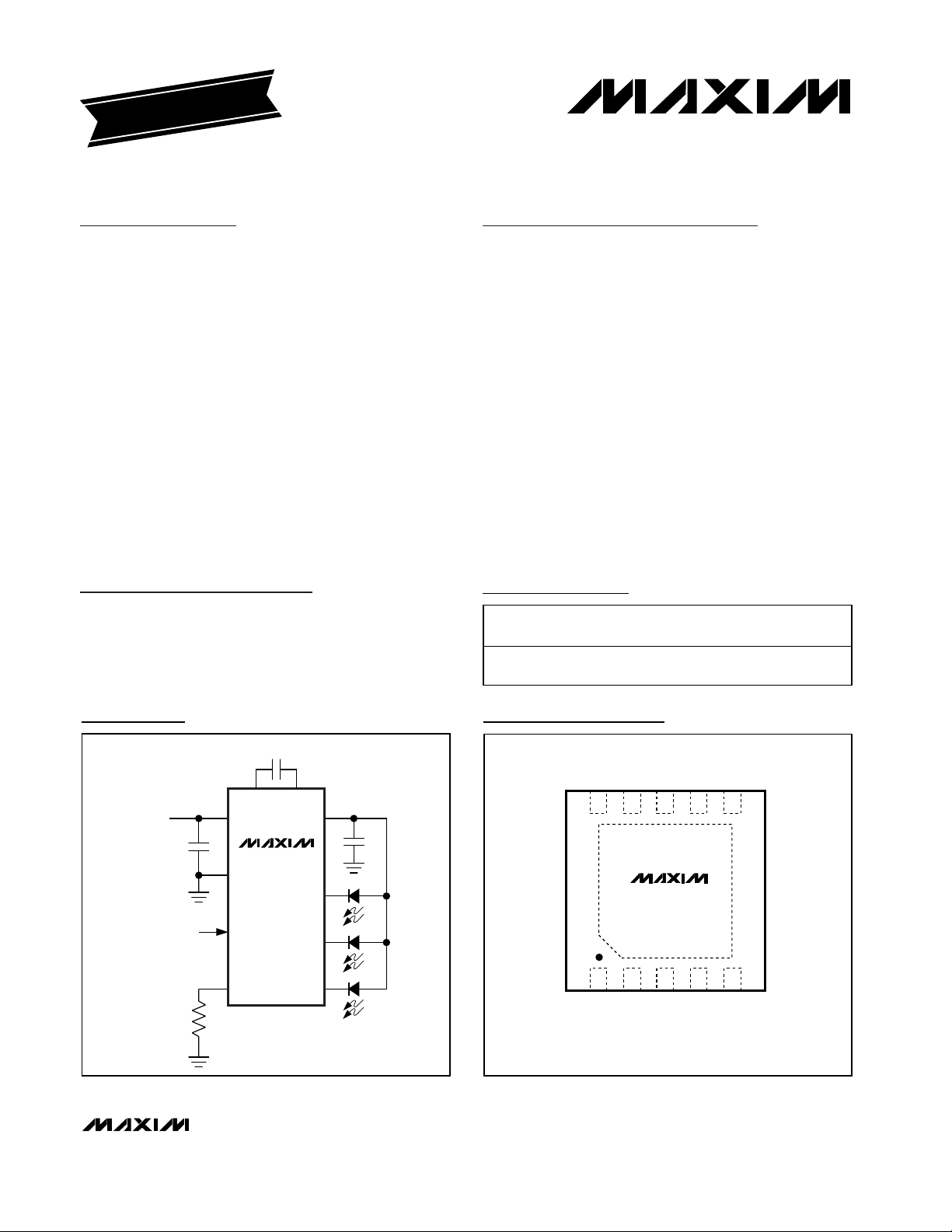
Pin Configuration
Ordering Information
1µF
1µF
MAX1574
LED3
LED2
LED1
OUT
SET
EN
GND
IN
0.22µF
CP CN
2.7V TO 5.5V
ON/OFF AND
DIMMING
UP TO 180mA
Typical Operating Circuit
19-3117; Rev 0; 12/03
For pricing, delivery, and ordering information, please contact Maxim/Dallas Direct! at
1-888-629-4642, or visit Maxim’s website at www.maxim-ic.com.
EVALUATION KIT
AVAILABLE
PART TEMP RANGE
MAX1574ETB -40°C to +85°C
PINPACKAGE
10 TDFN
3mm x 3mm
TOP
MARK
ABB
GND
LED1
LED26LED3
MAX1574
4
5
EN
CP
CN
SET
TDFN
3mm × 3mm
TOP VIEW
OUT
10 9 8 7
1234
IN
Page 2
MAX1574
180mA, 1x/2x, White LED Charge Pump
in 3mm x 3mm TDFN
2 _______________________________________________________________________________________
ABSOLUTE MAXIMUM RATINGS
ELECTRICAL CHARACTERISTICS
(VIN= 3.6V, V
GND
= 0V, EN = IN, R
SET
= 13.7kΩ, TA= -40°C to +85°C, unless otherwise noted. Typical values are at TA= +25°C.)
(Note 1)
Stresses beyond those listed under “Absolute Maximum Ratings” may cause permanent damage to the device. These are stress ratings only, and functional
operation of the device at these or any other conditions beyond those indicated in the operational sections of the specifications is not implied. Exposure to
absolute maximum rating conditions for extended periods may affect device reliability.
IN, OUT, EN to GND..............................................-0.3V to +6.0V
SET, LED1, LED2, LED3, CN to GND .........-0.3V to (V
IN
+ 0.3V)
CP to GND ......................................................................-0.3V to
the greater of (V
OUT
+ 1V) or (V
IN
+ 1V)
OUT Short Circuit to GND ..........................................Continuous
Continuous Power Dissipation (TA = +70°C)
10-Pin TDFN (derate 18.2mW/°C above +70°C) .......1454mW
Operating Temperature Range ...........................-40°C to +85°C
Junction Temperature......................................................+150°C
Storage Temperature Range .............................-65°C to +150°C
Lead Temperature (soldering, 10s) .................................+300°C
IN Operating Voltage 2.7 5.5 V
Undervoltage-Lockout Threshold VIN falling 2.25 2.45 2.60 V
Undervoltage-Lockout Hysteresis 40 mV
Output Overvoltage-Protection Threshold V
No-Load Supply Current
Shutdown Supply Current
Soft-Start Time 2ms
SET Bias Voltage 0.6 V
SET Leakage in Shutdown
SET Current Range 4 153 µA
SET-to-LED_ Current Ratio (I
LED Current Accuracy TA = +25°C ±0.7 %
LED-to-LED Current Matching (Note 2) -4 ±0.5 +4 %
Maximum LED_ Sink Current R
LED_ Dropout Voltage R
1x to 2x Mode Transition Threshold V
Input-Voltage-Mode Transition Hysteresis 150 mV
LED Leakage in Shutdown
Maximum OUT Current V
Open-Loop OUT Resistance
Switching Frequency 1 MHz
OUT Pulldown Resistance in Shutdown EN = GND 5 kΩ
EN High Voltage V
EN Low Voltage V
PARAMETER CONDITIONS MIN TYP MAX UNITS
LED/ISET
rising 5 V
OUT
2x mode 2
10% setting, 1x mode 0.35
EN = GND, TA = +25°C 0.01 1
EN = GND, T
EN = GND, TA = +25°C 0.01 1
EN = GND, T
) 100% setting 393 A/A
= 4.12kΩ 52 60 mA
SET
= 4.12kΩ (Note 3) 80 120 mV
SET
falling 120 130 140 mV
LED_
EN = GND, TA = +25°C 0.01 2
EN = GND, T
≥ 3.12V, V
IN
1x mode, (V
2x mode, (2 x V
= 2.7V to 5.5V 1.6 V
IN
= 2.7V to 5.5V 0.4 V
IN
IN
= +85°C 0.1
A
= +85°C 0.1
A
= +85°C 0.1
A
= 3.9V 180 mA
OUT
- V
IN
OUT
- V
) / I
OUT
OUT
) / I
OUT
1.5 2.5
915
mA
µA
µA
µA
Ω
Page 3
MAX1574
180mA, 1x/2x, White LED Charge Pump
in 3mm x 3mm TDFN
_______________________________________________________________________________________ 3
Note 1: Limits are 100% production tested at TA= +25°C. Limits over the operating temperature range are guaranteed by design.
Note 2: LED current matching is defined as: (I
LED
- I
AVG
) / I
AVG
Note 3: Dropout voltage is defined as the LED_-to-GND voltage at which current into LED_ drops 10% from the value at V
LED_
= 0.2V.
ELECTRICAL CHARACTERISTICS (continued)
(VIN= 3.6V, V
GND
= 0V, EN = IN, R
SET
= 13.7kΩ, TA= -40°C to +85°C, unless otherwise noted. Typical values are at TA= +25°C.)
(Note 1)
Typical Operating Characteristics
(Circuit of Figure 2, VIN= 3.6V, EN = IN, driving three white LEDs, TA= +25°C, unless otherwise noted.)
EFFICIENCY vs. INPUT VOLTAGE
MAX1574 toc01
INPUT VOLTAGE (V)
EFFICIENCY (%)
3.93.63.33.0
10
20
30
40
50
60
70
80
90
100
0
2.7 4.2
I
LED
= 2mA
I
LED
= 8mA
I
LED
= 20mA
I
LED
= 40mA
VIN FALLING
INPUT CURRENT vs. INPUT VOLTAGE
MAX1574 toc02
INPUT VOLTAGE (V)
INPUT CURRENT (mA)
3.93.63.33.0
50
100
150
200
250
300
0
2.7 4.2
VIN FALLING
I
LED
= 40mA
I
LED
= 20mA
I
LED
= 8mA
I
LED
= 2mA
INPUT RIPPLE vs. SUPPLY VOLTAGE
MAX1574 toc03
SUPPLY VOLTAGE (V)
INPUT RIPPLE (mV
P-P
)
5.04.54.03.53.0
5
10
15
20
25
0
2.5 5.5
60mA/LED
20mA/LED
8mA/LED
2mA/LED
EN Input Current
EN Low Shutdown Delay 1.0 2 3.3 ms
EN tLO (Figure 1) 0.5 500 µs
EN tHI (Figure 1) 0.5 µs
Initial EN tHI (Figure 1) Only required for first EN_ pulse 50 µs
Thermal-Shutdown Threshold +160 °C
Thermal-Shutdown Hysteresis 20 °C
PARAMETER CONDITIONS MIN TYP MAX UNITS
EN = GND or 5.5V, TA = +25°C 0.01 1
EN = GND or 5.5V, T
= +85°C 0.1
A
µA
Page 4

MAX1574
180mA, 1x/2x, White LED Charge Pump
in 3mm x 3mm TDFN
4 _______________________________________________________________________________________
Typical Operating Characteristics (continued)
(Circuit of Figure 2, VIN= 3.6V, EN = IN, driving three white LEDs, TA= +25°C, unless otherwise noted.)
LED CURRENT MATCHING
vs. INPUT SUPPLY VOLTAGE
MAX1574 toc04
INPUT SUPPLY VOLTAGE (V)
LED CURRENT MATCHING (%)
5.14.73.9 4.33.53.1
-0.8
-0.6
-0.4
-0.2
0
0.2
0.4
0.6
0.8
1.0
-1.0
2.7 5.5
I
LED
= 8mA
LED CURRENT vs. TEMPERATURE
MAX1574 toc05
TEMPERATURE (°C)
LED CURRENT (mA)
6035-15 10
7.85
7.90
7.95
8.00
8.05
8.10
8.15
8.20
7.80
-40 85
LED CURRENT vs. R
SET
MAX1574 toc06
R
SET
(kΩ)
LED CURRENT (mA)
10010
10
10001
100
1
100% BRIGHTNESS
SETTING
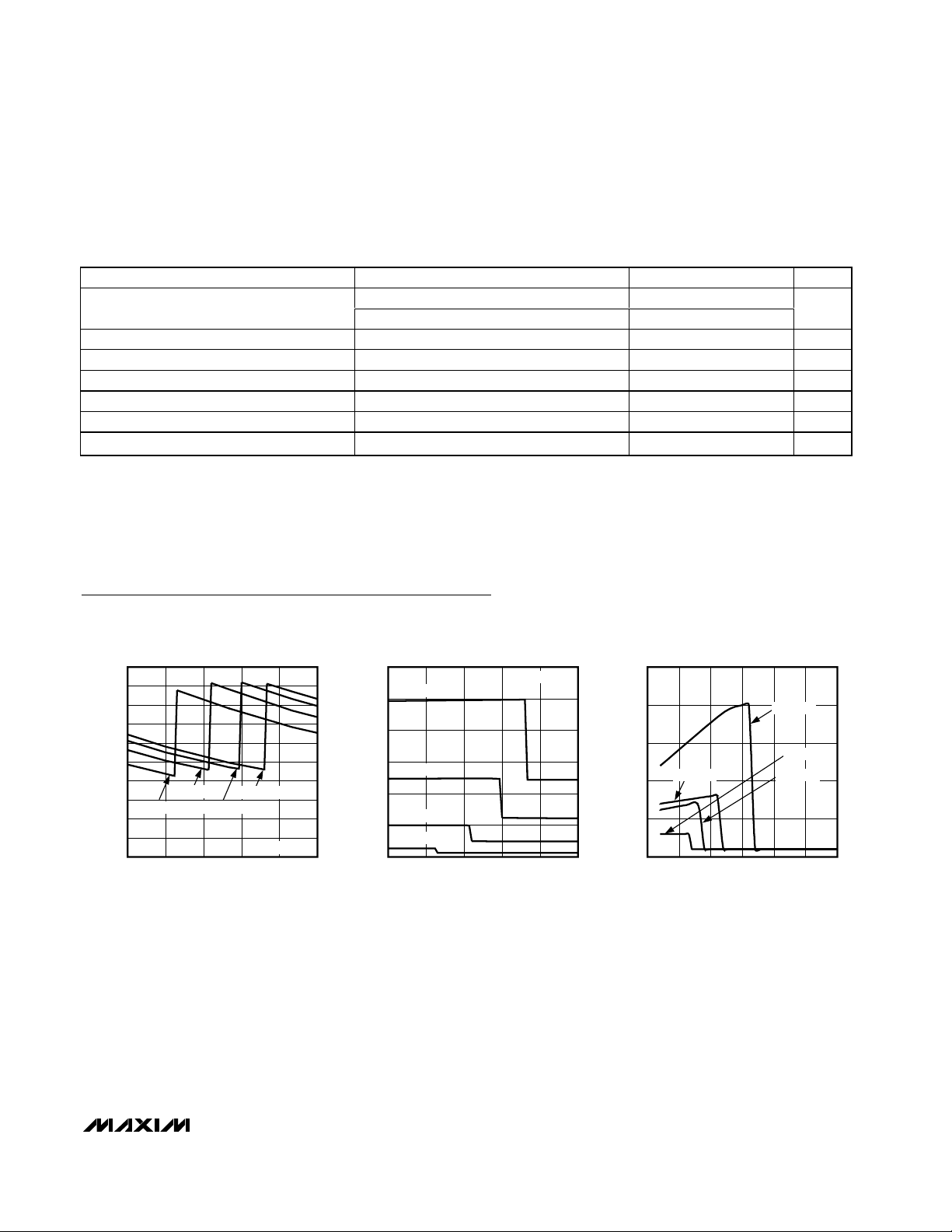
OPERATING WAVEFORMS (1x)
MAX1574 toc07
V
IN
V
OUT
I
IN
20mV/div
AC-COUPLED
50mV/div
AC-COUPLED
0mA
50mA/div
400ns/div
OPERATING WAVEFORMS (2x)
MAX1574 toc08
V
IN
V
OUT
I
IN
20mV/div
AC-COUPLED
50mV/div
AC-COUPLED
0mA
400ns/div
50mA/div
STARTUP AND SHUTDOWN
MAX1574 toc09
I
IN
V
EN
V
OUT
100mA/div
0mA
0V
5V/div
2V/div
1ms/div
Page 5

MAX1574
180mA, 1x/2x, White LED Charge Pump
in 3mm x 3mm TDFN
_______________________________________________________________________________________ 5
Typical Operating Characteristics (continued)
(Circuit of Figure 2, VIN= 3.6V, EN = IN, driving three white LEDs, TA= +25°C, unless otherwise noted.)
DIMMING RESPONSE
MAX1574 toc10
I
OUT
V
EN
V
OUT
50mA/div
2V/div
2V/div
10ms/div
LINE TRANSIENT 3.8V TO 3.3V TO 3.8V
MAX1574 toc11
V
OUT
V
IN
I
OUT
1V/div
1V/div
60mA,
20mA/div
100µs/div
Pin Description
)
PIN NAME FUNCTION
1IN
Supply Voltage Input. Connect a 0.47µF to 1µF ceramic capacitor from IN to GND. The input voltage
range is 2.7V to 5.5V. IN is high impedance during shutdown.
Enable and Dimming Control. Pulsing EN low dims the LEDs in multiple steps. Drive low for longer than
2EN
2ms (typ) to shut down the IC. From shutdown, drive EN high (50µs min) to set I
current (see the SETfunction). Pulse EN low for 0.5µs to 500µs to dim the LEDs (Figure 1).
3CPTransfer-Capacitor Positive Connection. Connect a 0.22µF capacitor from CP to CN.
4CNTransfer-Capacitor Negative Connection. Connect a 0.22µF capacitor from CP to CN.
5 SET
6 LED3
7 LED2
8 LED1
Current-Set Input. Connect a resistor (R
I
LED(MAX
= 393 × 0.6V / R
. SET is internally biased to 0.6V. SET is high impedance during shutdown.
SET
LED_ Cathode Connection. Current flowing into LED_ is based on SET description above. In 2x mode,
the charge pump regulates the lowest LED_ voltage to 0.18V. Connect LED_ to IN for unpopulated LEDs.
LED_ is high impedance during shutdown.
) from SET to GND to set the maximum LED current.
SET
9 GND Ground. Connect GND to system ground and as close as possible to the input-bypass capacitor ground.
10 OUT
Output. Connect a 0.47µF to 1µF ceramic capacitor from OUT to GND, and connect OUT to the anodes
of all the LEDs. OUT is pulled to ground through an internal 5kΩ
resistor in shutdown.
—EPExposed Paddle. Connect the exposed paddle directly to GND underneath the IC.
to the maximum
LED
Page 6

MAX1574
Detailed Description
The MAX1574 charge pump drives up to three white
LEDs with regulated constant current for uniform intensity. By utilizing adaptive 1x/2x charge-pump modes
and very-low-dropout current regulators, it achieves
180mA output drive capability and high efficiency over
the 1-cell lithium-battery input voltage range. Fixed-frequency switching of 1MHz allows for tiny external components, and the regulation scheme is optimized to
ensure low EMI and low input ripple.
1x to 2x Switchover
When VINis higher than V
OUT
, the MAX1574 operates in
1x mode and V
OUT
is pulled up to VIN. The internal current regulators regulate the LED current. As VINdrops,
V
LED_
eventually falls below the switchover threshold of
130mV, and the MAX1574 starts switching in 2x mode.
When the input voltage rises above V
OUT
by approxi-
mately 50mV, the MAX1574 switches back to 1x mode.
Soft-Start
The MAX1574 includes soft-start circuitry to limit inrush
current at turn-on. When starting up, the output capacitor
is charged directly from the input with a ramped current
source (with no charge-pump action) until the output voltage approaches the input voltage. Once this occurs, the
charge pump determines if 1x or 2x mode is required. In
the case of 1x mode, the soft-start is terminated and normal operation begins. During the soft-start time, the output current is set to 5% of the maximum set by R
SET
. In
the case of 2x mode, soft-start operates until the lowest of
LED1 to LED3 reaches regulation. If an overload condition occurs, soft-start repeats every 2.1ms. If the output is
shorted to ground, the output current is limited by the
MAX1574 switching technique.
Setting the Output Current
The LED current at full brightness is set by a resistor,
R
SET
, as follows:
EN Dimming Control
When the LEDs are enabled by driving EN high, the
MAX1574 goes through soft-start, bringing the LED current up to I
LED_
. Dimming is then done by pulsing EN
low (500ns to 500µs pulse width). Each pulse reduces
the LED current by 10%, so after one pulse the LED current is 0.9 x I
LED
. The tenth pulse reduces the current by
5%, so the I
LED_
current reduces from 0.1 x I
LED_
to 0.05
x I
LED
. The eleventh pulse sets the LED current back to
I
LED_
. Figure 1 shows a timing diagram for EN.
If dimming control is not required, EN works as a simple
on/off control. Drive EN high to enable the LEDs, or
drive EN low for shutdown.
Shutdown Mode
When EN is held low for 2ms or longer, the MAX1574
is shut down and put in a low-current mode. OUT is
internally pulled to GND with 5kΩ during shutdown.
Overvoltage Protection
If any LED fails as an open circuit, the output voltage is
limited to about 5V by gating on/off the charge pump.
If any LED_ is floating or grounded, the MAX1574 operates in the same overvoltage-protection mode. To avoid
overvoltage-protection mode when using fewer than
three LEDs, connect any unused LED_ to IN (Figure 3).
Thermal Shutdown
The MAX1574 includes a thermal-limit circuit that shuts
down the IC at approximately +160°C. The part turns on
after the IC cools by approximately 20°C.
R
V
I
SET
LED
.
_
=
×06 393
180mA, 1x/2x, White LED Charge Pump
in 3mm x 3mm TDFN
6 _______________________________________________________________________________________
Figure 1. EN Timing Diagram
INITIAL t
HI
≥ 50µs
0
EN
t
SOFT-START
100%
I
LED_
SHDN
1 111098765432
t
t
LO
90%
80%
70%
60%
50%
HI
5%
100%
90%
≥ 500ns500ns TO 500µs
40%
30%
20%
10%
t
SHDN
2ms (typ)
SHDN
Page 7

Applications Information
Driving Fewer than Three LEDs
When driving fewer than three LEDs, connect any unused
LED_ directly to IN (Figure 3). When connected in this
manner, the corresponding LED driver is disabled.
Driving Camera Strobes/Flashes
The MAX1574’s 180mA output capability makes it suitable for driving white LED camera strobes/flashes. For
example, the typical operating circuit drives a 3-LED
flash module with up to 60mA/LED. To ensure 180mA
total drive capability at low input voltages, increase C1
to 0.47µF.
To drive fewer or more LEDs with regulated total current up to 180mA or to reduce the number of connecting wires, short LED1, LED2, and LED3 together. When
connected this way, some LED modules have good
LED-to-LED forward-voltage matching, while others
may require individual ballast resistors. It is a good
idea to keep the ballast resistance as low as practical
for reasonable matching because high-ballast resistance reduces the output drive capability due to the
higher V
OUT
requirement.
Input Ripple
For LED drivers, input ripple is more important than output ripple. Input ripple depends on the source supply’s
impedance. Adding a lowpass filter to the input further
reduces input ripple. Alternatively, increasing CINto
2.2µF cuts input ripple in half with only a small increase in
footprint. The 1x mode always has very low input ripple.
Component Selection
Use only ceramic capacitors with an X5R, X7R, or better
dielectric. See Table 1 for a list of recommended parts.
PC Board Layout and Routing
The MAX1574 is a high-frequency switched-capacitor
voltage regulator. For best circuit performance, use a
solid ground plane and place CIN, C
OUT
, and C1 as
close to the MAX1574 as possible. Refer to the
MAX1574 evaluation kit for an example.
MAX1574
180mA, 1x/2x, White LED Charge Pump
in 3mm x 3mm TDFN
_______________________________________________________________________________________ 7
Table 1. Recommended Components
COMPONENT
DESIGNATION
CIN, C
OUT
C1
D1, D2, D3 —
R
SET
VALUE MANUFACTURER PART NUMBER DESCRIPTION
1µF
0.22µF
0.47µF
As Required
Taiyo Yuden JMK107BJ105KA 1µF ±10%, 6.3V X5R ceramic capacitors (0603)
TDK C1005X5R0J105M 1µF ±20%, 6.3V X5R ceramic capacitors (0402)
Taiyo Yuden JMK105BJ224KV 0.22µF ±10%, 6.3V X5R ceramic capacitor (0402)
TDK C1005X5R0J224K 0.22µF ±10%, 6.3V X5R ceramic capacitor (0402)
Taiyo Yuden JMK105BJ474KV 0.47µF ±10%, 6.3V X5R ceramic capacitor (0402)
TDK C1005X5R0J474K 0.47µF ±10%, 6.3V X5R ceramic capacitor (0402)
Nichia NSCW215T White LEDs
Citizen CL-470S White LED flash module
Kamaya
Panasonic
— 1% resistor
Page 8

MAX1574
Chip Information
TRANSISTOR COUNT: 6063
PROCESS: BiCMOS
180mA, 1x/2x, White LED Charge Pump
in 3mm x 3mm TDFN
8 _______________________________________________________________________________________
Figure 2. Functional Diagram and Typical Application Circuit
Figure 3. Using the MAX1574 to Drive Fewer Than Three LEDs
C1
0.22µF OR 0.47µF
CN
2.7V TO 5.5V
CONTROL AND
ENABLE
OFF
C
1µF
IN
IN
EN
ON
CONTROL AND
REFERENCEDIMMING
CONTROLLED-CURRENT
MIRROR
CP
1x/2x REGULATING CHARGE PUMP
ERROR
AMP1
0.18V
0.6V
SELMIN
OVD
1.25V
OUT
LED1
LED2
C
1µF
OUT
D1
D2
ERROR
AMP2
SET
R
SET
MAX1574
0.22µF
2.7V TO 5.5V
1µF
CP CN
IN
OUT
1µF
MAX1574
GND
LED1
ON/OFF AND
DIMMING
EN
LED2
GND
LED3
D3
SET
LED3
Page 9

MAX1574
180mA, 1x/2x, White LED Charge Pump
in 3mm x 3mm TDFN
Maxim cannot assume responsibility for use of any circuitry other than circuitry entirely embodied in a Maxim product. No circuit patent licenses are
implied. Maxim reserves the right to change the circuitry and specifications without notice at any time.
Maxim Integrated Products, 120 San Gabriel Drive, Sunnyvale, CA 94086 408-737-7600 _____________________ 9
© 2003 Maxim Integrated Products Printed USA is a registered trademark of Maxim Integrated Products.
Package Information
(The package drawing(s) in this data sheet may not reflect the most current specifications. For the latest package outline information,
go to www.maxim-ic.com/packages.)
L
PIN 1 ID
1N1
[(N/2)-1] x e
REF.
k
L
21-0137 D
6, 8, &10L, DFN THIN.EPS
1
2
PIN 1
INDEX
AREA
D
E
A
NUMBER OF LEADS SHOWN ARE FOR REFERENCE ONLY
A
A1
A2
L
DETAIL A
D2
b
E2
C
L
e
C0.35
e
e
DALLAS
SEMICONDUCTOR
PROPRIETARY INFORMATION
TITLE:
PACKAGE OUTLINE, 6, 8 & 10L,
TDFN, EXPOSED PAD, 3x3x0.80 mm
APPROVAL
C
L
DOCUMENT CONTROL NO. REV.
COMMON DIMENSIONS
MIN. MAX.
SYMBOL
0.70 0.80
A
2.90 3.10
D
2.90 3.10
E
0.00 0.05
A1
L
0.20 0.40
k
0.25 MIN.
A2 0.20 REF.
PACKAGE VARIATIONS
PKG. CODE
T633-1 1.50±0.10D22.30±0.10
N
6
1.50±0.10
E2
2.30±0.10T833-1 8
JEDEC SPEC
0.95 BSCeMO229 / WEEA
MO229 / WEEC
0.65 BSC
[(N/2)-1] x e
0.40±0.05b1.90 REF
1.95 REF0.30±0.05
0.25±0.05 2.00 REFMO229 / WEED-30.50 BSC1.50±0.10 2.30±0.1010T1033-1
DALLAS
SEMICONDUCTOR
PROPRIETARY INFORMATION
TITLE:
PACKAGE OUTLINE, 6, 8 & 10L,
TDFN, EXPOSED PAD, 3x3x0.80 mm
DOCUMENT CONTROL NO.APPROVAL
21-0137
REV.
2
2
D
 Loading...