

Page 1
General Description
The MAX1556/MAX1557 are low-operating-current
(16µA), fixed-frequency step-down regulators. High efficiency, low-quiescent operating current, low dropout,
and minimal (27µA) quiescent current in dropout make
these converters ideal for powering portable devices
from 1-cell Li-ion or 3-cell alkaline/NiMH batteries. The
MAX1556 delivers up to 1.2A; has pin-selectable 1.8V,
2.5V, and 3.3V outputs; and is also adjustable. The
MAX1557 delivers up to 600mA; has pin-selectable 1V,
1.3V, and 1.5V outputs; and is also adjustable.
The MAX1556/MAX1557 contain a low-on-resistance
internal MOSFET switch and synchronous rectifier to
maximize efficiency and dropout performance while
minimizing external component count. A proprietary
topology offers the benefits of a high fixed-frequency
operation while still providing excellent efficiency at
both light and full loads. A 1MHz PWM switching frequency keeps components small. Both devices also
feature an adjustable soft-start to minimize battery transient loading.
The MAX1556/MAX1557 are available in a tiny 10-pin
TDFN (3mm x 3mm) package.
Applications
PDAs and Palmtop Computers
Cell Phones and Smart Phones
Digital Cameras and Camcorders
Portable MP3 and DVD Players
Hand-Held Instruments
Features
♦ Up to 97% Efficiency
♦ 95% Efficiency at 1mA Load Current
♦ Low 16µA Quiescent Current
♦ 1MHz PWM Switching
♦ Tiny 3.3µH Inductor
♦ Selectable 3.3V, 2.5V, 1.8V, 1.5V, 1.3V, 1.0V, and
Adjustable Output
♦ 1.2A Guaranteed Output Current (MAX1556)
♦ Voltage Positioning Optimizes Load-Transient
Response
♦ Low 27µA Quiescent Current in Dropout
♦ Low 0.1µA Shutdown Current
♦ No External Schottky Diode Required
♦ Analog Soft-Start with Zero Overshoot Current
♦ Small, 10-Pin, 3mm x 3mm TDFN Package
MAX1556/MAX1557
16µA IQ, 1.2A PWM
Step-Down DC-DC Converters
________________________________________________________________ Maxim Integrated Products 1
TOP VIEW
LX
OUT
SHDN
6
7
8
9
10
INP
D1
3
2
1
SS
GND
IN
5
PGND
D2
4
TDFN
MAX1556/
MAX1557
Pin Configuration
Ordering Information
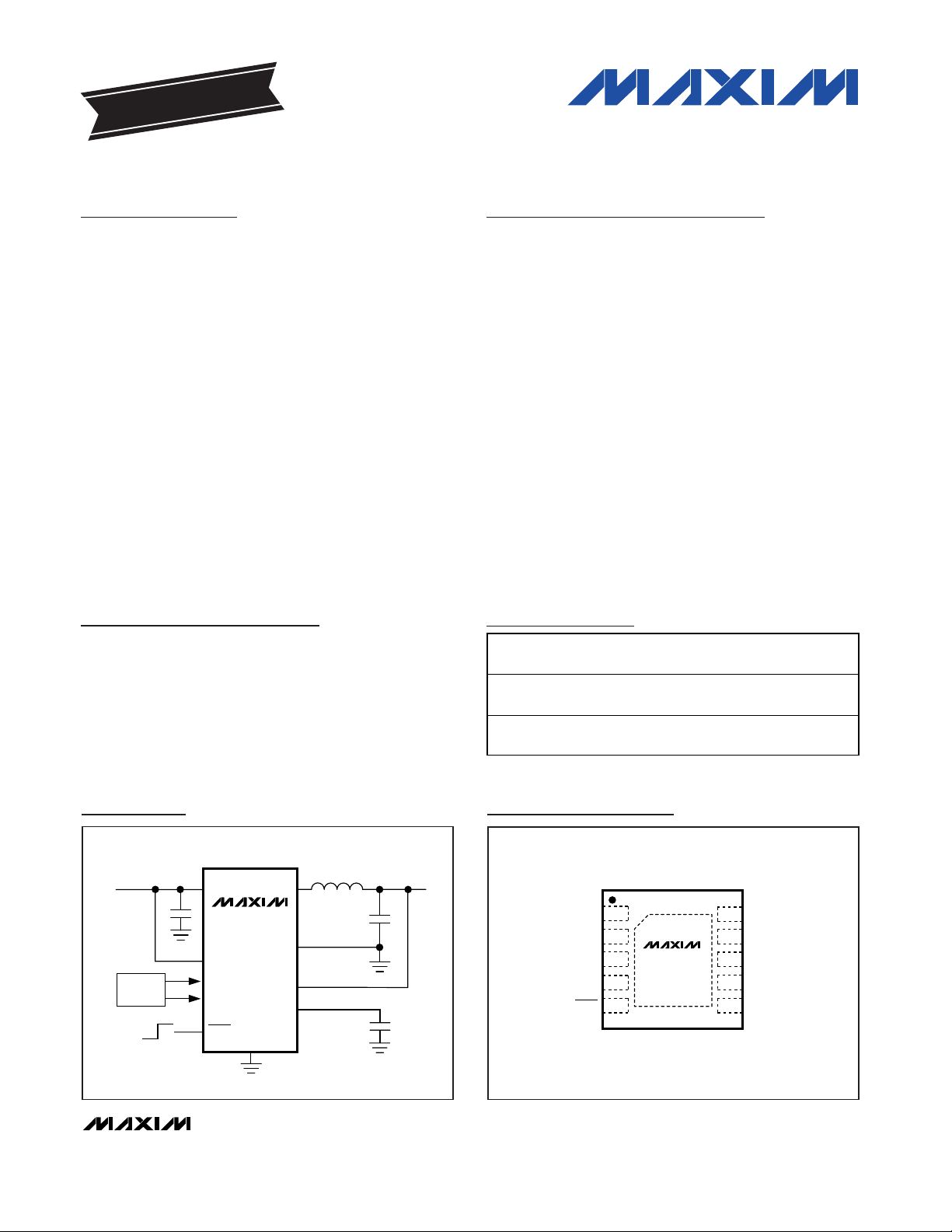
LX
SS
ON
OFF
SHDN
GND
INPUT
2.6V TO 5.5V
VOLTAGE
SELECT
OUTPUT
0.75V TO V
IN
PGND
OUT
INP
IN
D1
D2
MAX1556/
MAX1557
Typical Operating Circuit
19-3336; Rev 0; 7/04
For pricing, delivery, and ordering information, please contact Maxim/Dallas Direct! at
1-888-629-4642, or visit Maxim’s website at www.maxim-ic.com.
EVALUATION KIT
AVAILABLE
PART
TEMP RANGE
PIN-PACKAGE
TOP
MARK
MAX1556ETB
10 TDFN-EP*
(T1033-1)
ACQ
MAX1557ETB
10 TDFN-EP*
(T1033-1)
ACR
*EP = Exposed paddle.
-40°C to +85°C
-40°C to +85°C
Page 2
MAX1556/MAX1557
16µA IQ, 1.2A PWM DC-DC
Step-Down Converters
2 _______________________________________________________________________________________
ABSOLUTE MAXIMUM RATINGS
ELECTRICAL CHARACTERISTICS
(VIN= V
INP
= V
SHDN
= 3.6V, TA = - 40°C to +85°C. Typical values are at TA = +25°C, unless otherwise noted.) (Note 1)
Stresses beyond those listed under “Absolute Maximum Ratings” may cause permanent damage to the device. These are stress ratings only, and functional
operation of the device at these or any other conditions beyond those indicated in the operational sections of the specifications is not implied. Exposure to
absolute maximum rating conditions for extended periods may affect device reliability.
IN, INP, OUT, D2, SHDN to GND ..........................-0.3V to +6.0V
SS, D1 to GND.............................................-0.3V to (V
IN
+ 0.3V)
PGND to GND .......................................................-0.3V to +0.3V
LX Current (Note 1)...........................................................±2.25A
Output Short-Circuit Duration.....................................Continuous
Continuous Power Dissipation (T
A
= +70°C)
10-Pin TDFN (derate 24.4mW/°C above +70°C) .......1951mW
Operating Temperature Range ...........................-40°C to +85°C
Junction Temperature......................................................+150°C
Storage Temperature Range .............................-65°C to +150°C
Lead Temperature (soldering, 10s) .................................+300°C
PARAMETER CONDITIONS
UNITS
Input Voltage 2.6 5.5 V
Undervoltage-Lockout Threshold
VIN rising and falling, 35mV hysteresis (typ)
V
No switching, D1 = D2 = GND 16 25
Quiescent Supply Current
Dropout 27 42
µA
TA = +25°C 0.1 1
Shutdown Supply Current SHDN = GND
T
A
= +85°C 0.1
µA
Output Voltage Range
V
IN
V
No load
300mA load
0
600mA load
0
TA = 0°C to +85°C
(Note 2)
1200mA load, MAX1556 only
No load
300mA load
600mA load
Output Accuracy
T
A
= -40°C to +85°C
(Note 2)
1200mA load, MAX1556 only
%
MAX1556
Maximum Output Current
MAX1557
mA
TA = +25°C
0.1
D1 = D2 = GND
T
A
= +85°C
OUT Bias Current
For preset output voltages 3 4.5
µA
No load
300mA load
0
600mA load
D1 = D2 = GND,
V
OUT
= 0.75V at
300mA (typ),
T
A
= 0°C to +85°C
1200mA load, MAX1556 only
No load
300mA load
600mA load
FB Threshold Accuracy
D1 = D2 = GND,
V
OUT
= 0.75V
at 300mA (typ),
T
A
= -40°C to +85°C
1200mA load, MAX1556 only
%
Note 1: LX has internal clamp diodes to GND and IN. Applications that forward bias these diodes should take care not to exceed
the IC’s package power-dissipation limits.
MIN TYP MAX
2.20 2.35 2.55
0.75
-0.25 +0.75 +1.75
-0.75
-1.5 -0.75
-2.75 -2.25 -1.25
-0.75 +2.25
-1.5 +1.5
-2.25 +0.50
-4.0 -1.0
1200
600
0.01
0.01
-0.50 +0.75 +1.75
-1.2
-1.75 -0.75 +0.25
-3.25 -2.25 -1.25
-1.25 +2.25
-1.75 +1.50
-2.75 +0.25
-4.25 -1.00
+0.75
+1.2
Page 3
MAX1556/MAX1557
16µA IQ, 1.2A PWM DC-DC
Step-Down Converters
_______________________________________________________________________________________ 3
Note 1: All units are 100% production tested at TA= +25°C. Limits over the operating range are guaranteed by design.
Note 2: For the MAX1556, 3.3V output accuracy is specified with a 4.2V input.
ELECTRICAL CHARACTERISTICS (continued)
(VIN= V
INP
= V
SHDN
= 3.6V, TA = - 40°C to +85°C. Typical values are at TA = +25°C, unless otherwise noted.) (Note 1)
PARAMETER CONDITIONS
MIN
TYP
MAX
UNITS
VIN = 2.6V to 3.6V
MAX1556,
D1 = IN, D2 = GND
V
IN
= 3.6V to 5.5V
VIN = 2.6V to 3.6V
Line Regulation
MAX1557,
D1 = IN, D2 = GND
V
IN
= 3.6V to 5.5V
%
VIN = 3.6V
MAX1556
V
IN
= 2.6V
VIN = 3.6V
0.7
p-Channel On-Resistance
MAX1557
V
IN
= 2.6V
Ω
VIN = 3.6V
n-Channel On-Resistance
V
IN
= 2.6V
Ω
MAX1556 1.5 1.8 2.1
p-Channel Current-Limit
Threshold
MAX1557 0.8 1.0 1.2
A
n-Channel Zero Crossing
Threshold
20 35 45 mA
MAX1556 1.8
RMS LX Output Current
MAX1557 1.0
TA = +25°C 0.1 10
LX Leakage Current
V
IN
= 5.5V, LX =
GND or IN
T
A
= +85°C 0.1
µA
Maximum Duty Cycle
%
Minimum Duty Cycle 0%
Internal Oscillator Frequency 0.9 1 1.1
SS Output Impedance ∆VSS / ISS for ISS = 2µA
300 kΩ
SS Discharge Resistance SHDN = GND, 1mA sink current 90 200 Ω
Thermal-Shutdown Threshold
°C
Thermal-Shutdown Hysteresis 15 °C
LOGIC INPUTS (D1, D2, SHDN)
Input-Voltage High 2.6V ≤ VIN ≤ 5.5V 1.4 V
Input-Voltage Low 0.4 V
TA = +25°C 0.1 1
Input Leakage
T
A
= +85°C 0.1
µA
-0.37
0.33
-0.1
0.09
0.19 0.35
0.23
0.35
0.42
0.27 0.48
0.33
100
130 200
+160
A
RMS
MHz
Page 4
MAX1556/MAX1557
16µA IQ, 1.2A PWM DC-DC
Step-Down Converters
4 _______________________________________________________________________________________
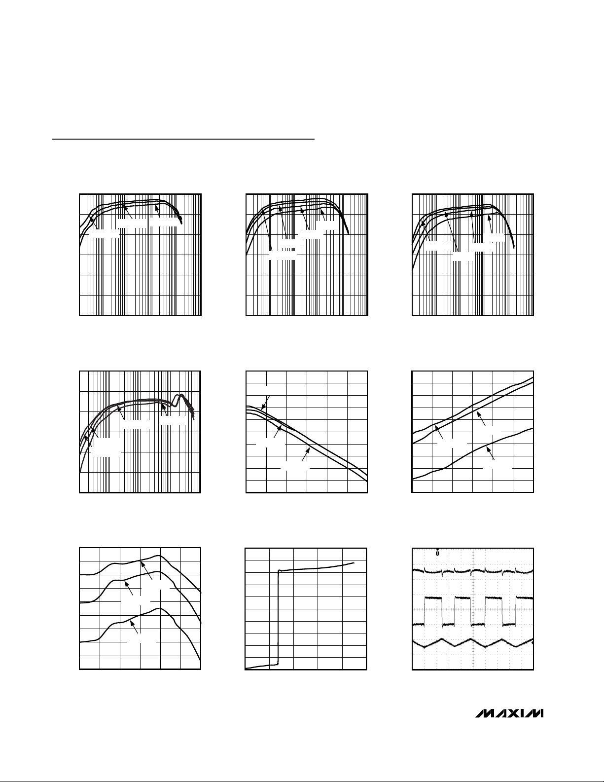
Typical Operating Characteristics
(VIN= V
INP
= 3.6V, D1 = D2 = SHDN = IN, Circuits of Figures 2 and 3, TA= +25°C, unless otherwise noted.)
EFFICIENCY vs. LOAD CURRENT
WITH 3.3V OUTPUT
MAX1556/7 toc01
LOAD CURRENT (mA)
EFFICIENCY (%)
100101
60
70
80
90
100
50
40
0.1 1000 10,000
VIN = 5V
VIN = 3.6V
VIN = 4.2V
EFFICIENCY vs. LOAD CURRENT
WITH 2.5V OUTPUT
MAX1556/7 toc02
LOAD CURRENT (mA)
EFFICIENCY (%)
100101
60
70
80
90
100
50
40
0.1 1000 10,000
VIN = 3.6V
VIN = 3V
VIN = 2.6V
VIN = 5V
EFFICIENCY vs. LOAD CURRENT
WITH 1.8V OUTPUT
MAX1556/7 toc03
LOAD CURRENT (mA)
EFFICIENCY (%)
100101
60
70
80
90
100
50
40
0.1 1000 10,000
VIN = 5V
VIN = 3.6V
VIN = 3V
VIN = 2.6V
EFFICIENCY vs. LOAD CURRENT
WITH 1.0V OUTPUT (MAX1557)
MAX1556/7 toc04
LOAD CURRENT (mA)
EFFICIENCY (%)
100101
60
70
80
90
100
50
40
0.1 1000
VIN = 5V
VIN = 3.6V
VIN = 3V
VIN = 2.6V
OUTPUT VOLTAGE
vs. LOAD CURRENT
MAX1556/7 toc05
LOAD CURRENT (mA)
OUTPUT VOLTAGE (V)
1000800600400200
1.75
1.76
1.77
1.78
1.79
1.80
1.81
1.82
1.83
1.84
1.74
01200
TA = -45°C
TA = +25°C
TA = +85°C
OUTPUT VOLTAGE vs. INPUT VOLTAGE
WITH 600mA LOAD
MAX1556/7 toc06
INPUT VOLTAGE (V)
OUTPUT VOLTAGE (V)
5.04.54.03.53.0
1.780
1.781
1.782
1.783
1.784
1.785
1.786
1.787
1.788
1.789
1.779
2.5 5.5
TA = -40°C
TA = +25°C
TA = +85°C
OUTPUT VOLTAGE vs. INPUT VOLTAGE
WITH NO LOAD
MAX1556/7 toc07
INPUT VOLTAGE (V)
OUTPUT VOLTAGE (V)
5.04.54.03.53.0
1.804
1.805
1.806
1.807
1.808
1.809
1.810
1.811
1.812
1.803
2.5 5.5
TA = -40°C
TA = +25°C
TA = +85°C
SUPPLY CURRENT vs. INPUT VOLTAGE
MAX1556/7 toc08
INPUT VOLTAGE (V)
SUPPLY CURRENT (µA)
5432
2
4
6
8
10
12
14
16
18
20
0
16
HEAVY-LOAD SWITCHING WAVEFORMS
MAX1556/7 toc09
V
OUT
AC-COUPLED
10mV/div
V
LX
I
LX
2V/div
0
0
400ns
500mA/div
I
LOAD
= 750mA
Page 5

MAX1556/MAX1557
16µA IQ, 1.2A PWM DC-DC
Step-Down Converters
_______________________________________________________________________________________ 5
LIGHT-LOAD SWITCHING WAVEFORMS
MAX1556/7 toc10
20mV/div
AC-COUPLED
V
LX
V
OUT
I
LX
2V/div
0
4µs/div
0
200mA/div
SOFT-START/SHUTDOWN WAVEFORMS
MAX1556/7 toc11
5V/div
I
LX
V
SHDN
V
OUT
I
IN
500mA/div
0
0
100µs/div
0
1V/div
0
500mA/div
CSS = 470pF
R
LOAD
= 4Ω
SOFT-START RAMP TIME vs. C
SS
MAX1556/7 toc12
CSS (pF)
SOFT-START RAMP TIME (ms)
500 1000 1500 2000
1
10
0.1
02500
LOAD TRANSIENT
MAX1556/7 toc13
50mV/div
AC-COUPLED
500mA/div
V
OUT
I
OUT
20µs/div
0
I
OUTMIN
= 20mA
LOAD TRANSIENT
MAX1556/7 toc14
50mV/div
AC-COUPLED
500mA/div
V
OUT
I
OUT
20µs/div
0
I
OUTMIN
= 180mA
LINE TRANSIENT
MAX1556/7 toc15
10mV/div
AC-COUPLED
V
IN
V
OUT
I
LX
3.5V
4V
40µs/div
0
200mA/div
BODE PLOT
MAX1556/7 toc16
FREQUENCY (kHz)
GAIN (dB)
PHASE (DEGREES)
100101
-50
-40
-30
-20
-10
0
10
20
30
40
-60
-30
0
30
60
90
120
150
180
210
240
-60
0.1 1000
0dB
PHASE MARGIN = 53°
C
OUT
= 22µF, R
LOAD
= 4Ω
Typical Operating Characteristics (continued)
(VIN= V
INP
= 3.6V, D1 = D2 = SHDN = IN, Circuits of Figures 2 and 3, TA= +25°C, unless otherwise noted.)
Page 6

MAX1556/MAX1557
16µA IQ, 1.2A PWM DC-DC
Step-Down Converters
6 _______________________________________________________________________________________
Detailed Description
The MAX1556/MAX1557 synchronous step-down converters deliver a guaranteed 1.2A/600mA at output voltages from 0.75V to VIN. They use a 1MHz PWM
current-mode control scheme with internal compensation,
allowing for tiny external components and a fast transient
response. At light loads the MAX1556/MAX1557 automatically switch to pulse-skipping mode to keep the quiescent supply current as low as 16µA. Figures 2 and 3
show the typical application circuits.
Control Scheme
During PWM operation the converters use a fixed-frequency, current-mode control scheme. The heart of the
current-mode PWM controller is an open-loop, multipleinput comparator that compares the error-amp voltage
feedback signal against the sum of the amplified current-sense signal and the slope-compensation ramp. At
the beginning of each clock cycle, the internal high-side
p-channel MOSFET turns on until the PWM comparator
trips. During this time the current in the inductor ramps
up, sourcing current to the output and storing energy in
the inductor’s magnetic field. When the p-channel turns
off, the internal low-side n-channel MOSFET turns on.
Now the inductor releases the stored energy while the
current ramps down, still providing current to the output.
The output capacitor stores charge when the inductor
current exceeds the load and discharges when the
inductor current is lower than the load. Under overload
conditions, when the inductor current exceeds the current limit, the high-side MOSFET is turned off and the
low-side MOSFET remains on until the next clock cycle.
Pin Description
PIN NAME FUNCTION
1INSupply Voltage Input. Connect to a 2.6V to 5.5V source.
2 GND Ground. Connect to PGND.
3SS
Soft-Start Control. Connect a 1000pF capacitor (C
SS
) from SS to GND to eliminate input-current
overshoot during startup. C
SS
is required for normal operation of the MAX1556/MAX1557. For greater
than 22µF total output capacitance, increase C
SS
to C
OUT
/ 22,000 for soft-start. SS is internally
discharged through 200Ω to GND in shutdown.
4 OUT
Output Sense Input. Connect to the output of the regulator. D1 and D2 select the desired output
voltage through an internal feedback resistor-divider. The internal feedback resistor-divider remains
connected in shutdown.
5 SHDN
Shutdown Input. Drive SHDN low to enable low-power shutdown mode. Drive high or connect to IN
for normal operation.
6D2OUT Voltage-Select Input. See Table 1.
7 PGND Power Ground. Connect to GND.
8LX
Inductor Connection. Connected to the drains of the internal power MOSFETs. High impedance in
shutdown mode.
9 INP
Supply Voltage, High-Current Input. Connect to a 2.6V to 5.5V source. Bypass with a 10µF ceramic
capacitor to PGND.
10 D1 OUT Voltage-Select Input. See Table 1.
EP —
Exposed Paddle. Connect to ground plane. EP also functions as a heatsink. Solder to circuit-board
ground plane to maximize thermal dissipation.
Table 1. Output-Voltage-Select Truth Table
A zero represents D_ being driven low or connected to GND.
A 1 represents D_ being driven high or connected to IN.
D1 D2 MAX1556 V
00 Adjustable from 0.75V to V
01 3.3V 1.5V
10 2.5V 1.3V
11 1.8V 1.0V
OUT
MAX1557 V
OUT
IN
Page 7

MAX1556/MAX1557
16µA IQ, 1.2A PWM DC-DC
Step-Down Converters
_______________________________________________________________________________________ 7
LX
SS
ON
OFF
SHDN
GND
INPUT
2.6V TO 5.5V
VOLTAGE
SELECT
OUTPUT
0.75V TO V
IN
PGND
C1
10µF
C4
0.47µF
R1
100Ω
C2
22µF
C3
1000pF
L1
3.3µH
OUT
INP
IN
1.2A
D1
D2
MAX1556
Figure 2. MAX1556 Typical Application Circuit
Figure 1. Functional Diagram
LX
SS
ON
OFF
SHDN
GND
INPUT
2.6V TO 5.5V
VOLTAGE
SELECT
OUTPUT
0.75V TO V
IN
PGND
C4
10µF
C5
22µF
C6
1000pF
L2
4.7µH
OUT
INP
IN
600mA
D1
D2
MAX1557
Figure 3. MAX1557 Typical Application Circuit
PWM
COMPARATOR
ERROR
AMPLIFIER
CURRENT-LIMIT
COMPARATOR
0.675V
CURRENT
SENSE
SLOPE
COMP
CLOCK
1MHz
INP
LX
PGND
SS
GND
PWM
AUTO SKIP
CONTROL
SKIP-OVER
ENTER SKIP/
SR OFF
V
CS
ZERO-CROSS
DETECT
SHORT-CIRCUIT
PROTECTION
REFERENCE
1.25V
OUT
D1
D2
SHDN
IN
BIAS
OUTPUT
VOLTAGE
SELECTOR
MAX1556
MAX1557
Page 8

As the load current decreases, the converters enter a
pulse-skip mode in which the PWM comparator is disabled. At light loads, efficency is enhanced by a
pulse-skip mode in which switching occurs only as
needed to service the load. Quiescent current in skip
mode is typically 16µA. See the Light-Load Switching
Waveforms and Load Transient graphs in the Typical
Operating Characteristics.
Load-Transient Response/
Voltage Positioning
The MAX1556/MAX1557 match the load regulation to
the voltage droop seen during transients. This is sometimes called voltage positioning. The load line used to
achieve this behavior is shown in Figures 4 and 5. There
is minimal overshoot when the load is removed and minimal voltage drop during a transition from light load to
full load. Additionally, the MAX1556 and MAX1557 use a
wide-bandwidth feedback loop to respond more quickly
to a load transient than regulators using conventional
integrating feedback loops (see Load Transient in the
Typical Operating Characteristics).
The MAX1556/MAX1557 use of a wide-band control
loop and voltage positioning allows superior load-transient response by minimizing the amplitude and duration of overshoot and undershoot in response to load
transients. Other DC-DC converters, with high gaincontrol loops, use external compensation to maintain
tight DC load regulation but still allow large voltage
droops of 5% or greater for several hundreds of
microseconds during transients. For example, if the
load is a CPU running at 600MHz, then a dip lasting
100µs corresponds to 60,000 CPU clock cycles.
Voltage positioning on the MAX1556/MAX1557 allows
up to 2.25% (typ) of load-regulation voltage shift but
has no further transient droop. Thus, during load transients, the voltage delivered to the CPU remains within
spec more effectively than with other regulators that
might have tighter initial DC accuracy. In summary, a
2.25% load regulation with no transient droop is much
better than a converter with 0.5% load regulation and
5% or more of voltage droop during load transients.
Load-transient variation can be seen only with an oscilloscope (see the Typical Operating Characteristics),
while DC load regulation read by a voltmeter does not
show how the power supply reacts to load transients.
Dropout/100% Duty-Cycle Operation
The MAX1556/MAX1557 function with a low input-to-output voltage difference by operating at 100% duty cycle.
In this state, the high-side p-channel MOSFET is always
on. This is particularly useful in battery-powered applications with a 3.3V output. The system and load might
operate normally down to 3V or less. The MAX1556/
MAX1557 allow the output to follow the input battery
voltage as it drops below the regulation voltage. The quiescent current in this state rises minimally to only 27µA
(typ), which aids in extending battery life. This
dropout/100% duty-cycle operation achieves long battery
life by taking full advantage of the entire battery range.
The input voltage required to maintain regulation is a
function of the output voltage and the load. The difference between this minimum input voltage and the output voltage is called the dropout voltage. The dropout
voltage is therefore a function of the on-resistance of
the internal p-channel MOSFET (R
DS(ON)P
) and the
inductor resistance (DCR).
V
DROPOUT
= I
OUT
x (R
DS(ON)P
+ DCR)
MAX1556/MAX1557
16µA IQ, 1.2A PWM DC-DC
Step-Down Converters
8 _______________________________________________________________________________________
-2.5
-1.5
-2.0
-0.5
-1.0
0.5
0
1.0
0
200
400
800
600
1000
1200
LOAD CURRENT (mA)
CHANGE IN OUTPUT VOLTAGE (%)
VIN = 3.6V
VIN = 5.5V
VIN = 2.6V
Figure 4. MAX1556 Voltage-Positioning Load Line
Figure 5. MAX1557 Voltage-Positioning Load Line
0 200 400 600
LOAD CURRENT (mA)
CHANGE IN OUTPUT VOLTAGE (%)
-1.0
-0.4
-0.6
-0.8
-0.2
0
0.2
0.4
0.6
0.8
1.0
VIN = 5.5V
VIN = 2.6V
VIN = 3.6V
Page 9

MAX1556/MAX1557
16µA IQ, 1.2A PWM DC-DC
Step-Down Converters
_______________________________________________________________________________________ 9
(R
DS(ON)P
) is given in the Electrical Characteristics. DCR
for a few recommended inductors is listed in Table 2.
Soft-Start
The MAX1556/MAX1557 use soft-start to eliminate
inrush current during startup, reducing transients at the
input source. Soft-start is particularly useful for higherimpedance input sources such as Li+ and alkaline
cells. Connect the required soft-start capacitor from SS
to GND. For most applications using a 22µF output
capacitor, connect a 1000pF capacitor from SS to
GND. If a larger output capacitor is used, then use the
following formula to find the value of the soft-start
capacitor:
Soft-start is implemented by exponentially ramping up
the output voltage from 0 to V
OUT(NOM)
with a time constant equal to CSStimes 200kΩ (see the Typical
Operating Characteristics). Assuming three time constants to full output voltage, use the following formula to
calculate the soft-start time:
Shutdown Mode
Connecting SHDN to GND or logic low places the
MAX1556/MAX1557 in shutdown mode and reduces
supply current to 0.1µA. In shutdown, the control circuitry and the internal p-channel and n-channel
MOSFETs turn off and LX becomes high impedance.
Connect SHDN to IN or logic high for normal operation.
Thermal Shutdown
As soon as the junction temperature of the
MAX1556/MAX1557 exceeds +160°C, the ICs go into
thermal shutdown. In this mode the internal p-channel
switch and the internal n-channel synchronous rectifier
are turned off. The device resumes normal operation
when the junction temperature falls below +145°C.
Applications Information
The MAX1556/MAX1557 are optimized for use with small
external components. The correct selection of inductors
and input and output capacitors ensures high efficiency,
low output ripple, and fast transient response.
Adjusting the Output Voltage
The adjustable output is selected when D1 = D2 = 0
and an external resistor-divider is used to set the output
voltage (see Figure 6). The MAX1556/MAX1557 have a
defined line- and load-regulation slope. The load regulation is for both preset and adjustable outputs and is
described in the Electrical Characteristics table and
Figures 4 and 5. The impact of the line-regulation slope
can be reduced by applying a correction factor to the
feedback resistor equation.
First, calculate the correction factor, k, by plugging the
desired output voltage into the following formula:
k represents the shift in the operating point at the feedback node (OUT).
Select the lower feedback resistor, R3, to be ≤35.7kΩ to
ensure stability and solve for R2:
075 3
32
.
Vk
V
R
RR
OUTPUT
−
=
+
()
kxVx
VV
V
OUTPUT
.
.
.
=
−
−
106 10
075
36
2
txxC
SS SS
= 600 10
3
C
C
SS
OUT
=
22000
Table 2. Inductor Selection
PART
DCR (mΩ)I
SAT
(mA) SIZE (mm) SHIELDED
Taiyo Yuden
3.3 36 1300 5 x 5 x 2.0 Yes
Taiyo Yuden
4.7 50 1200 5 x 5 x 2.0 Yes
TOKO D52LC 3.5 73 1340 5 x 5 x 2.0 Yes
TOKO D52LC 4.7 87 1140 5 x 5 x 2.0 Yes
Sumida CDRH3D16 4.7 50 1200
Yes
TOKO D412F 4.7 100* 1200*
Yes
Murata LQH32CN 4.7 97 790
No
Sumitomo CXL180 4.7 70* 1000*
No
Sumitomo CXLD140 4.7 100* 800*
No
*Estimated based upon similar-valued prototype inductors.
MANUFACTURER
LMNP04SB3R3N
LMNP04SB4R7N
VALUE (µH)
3.8 x 3.8 x 1.8
4.8 x 4.8 x 1.2
2.5 x 3.2 x 2.0
3.0 x 3.2 x 1.7
2.8 x 3.2 x 1.5
Page 10

MAX1556/MAX1557
Inductor Selection
A 4.7µH inductor with a saturation current of at least
800mA is recommended for the MAX1557 full-load
(600mA) application. For the MAX1556 application with
1.2A full load, use a 3.3µH inductor with at least 1.34A
saturation current. For lower full-load currents the
inductor current rating can be reduced. For maximum
efficiency, the inductor’s resistance (DCR) should be as
low as possible. Please note that the core material differs among different manufacturers and inductor types
and has an impact on the efficiency. See Table 2 for
recommended inductors and manufacturers.
Capacitor Selection
Ceramic input and output capacitors are recommended for most applications. For best stability over a wide
temperature range, use capacitors with an X5R or better dielectric due to their small size, low ESR, and low
temperature coefficients.
Output Capacitor
The output capacitor C
OUT
is required to keep the output voltage ripple small and to ensure regulation loop
stability. C
OUT
must have low impedance at the switching frequency. A 22µF ceramic output capacitor is recommended for most applications. If a larger output
capacitor is used, then paralleling smaller capacitors is
suggested to keep the effective impedance of the
capacitor low at the switching frequency.
Input Capacitor
Due to the pulsating nature of the input current in a buck
converter, a low-ESR input capacitor at INP is required
for input voltage filtering and to minimize interference
with other circuits. The impedance of the input capacitor
C
INP
should be kept very low at the switching frequency. A minimum value of 10µF is recommended at INP for
most applications. The input capacitor can be increased
for better input filtering.
IN Input Filter
In all MAX1557 applications, connect INP directly to IN
and bypass INP as described in the Input Capacitor section. No additional bypass capacitor is required at IN.
For applications using the MAX1556, an RC filter
between INP and IN keeps power-supply noise from
entering the IC. Connect a 100Ω resistor between INP
and IN, and connect a 0.47µF capacitor from IN to GND.
Soft-Start Capacitor
The soft-start capacitor, CSS, is required for proper
operation of the MAX1556/MAX1557. The recommended value of CSSis discussed in the Soft-Start section.
Soft-start times for various soft-start capacitors are
shown in the Typical Operating Characteristics.
PC Board Layout and Routing
Due to fast-switching waveforms and high-current
paths, careful PC board layout is required. An evaluation kit (MAX1556EVKIT) is available to speed design.
When laying out a board, minimize trace lengths
between the IC, the inductor, the input capacitor, and
the output capacitor. Keep these traces short, direct,
and wide. Keep noisy traces, such as the LX node
trace, away from OUT. The input bypass capacitors
should be placed as close to the IC as possible.
Connect GND to the exposed paddle and star PGND
and GND together at the output capacitor. The ground
connections of the input and output capacitors should
be as close together as possible.
Chip Information
TRANSISTOR COUNT: 7567
PROCESS: BiCMOS
16µA IQ, 1.2A PWM DC-DC
Step-Down Converters
10 ______________________________________________________________________________________
OUTPUT
OUT
R2
R3
SS
REFERENCE
1.25V
ERROR
AMPLIFIER
Figure 6. Adjustable Output Voltage
Page 11

MAX1556/MAX1557
16µA IQ, 1.2A PWM DC-DC
Step-Down Converters
______________________________________________________________________________________ 11
Package Information
(The package drawing(s) in this data sheet may not reflect the most current specifications. For the latest package outline information,
go to www.maxim-ic.com/packages
.
6, 8, &10L, DFN THIN.EPS
L
C
L
C
PIN 1
INDEX
AREA
D
E
L
e
L
A
e
NUMBER OF LEADS SHOWN ARE FOR REFERENCE ONLY
E2
DETAIL A
N
F
1
2
21-0137
PACKAGE OUTLINE, 6, 8, 10 & 14L,
TDFN, EXPOSED PAD, 3x3x0.80 mm
Page 12

MAX1556/MAX1557
16µA IQ, 1.2A PWM DC-DC
Step-Down Converters
Maxim cannot assume responsibility for use of any circuitry other than circuitry entirely embodied in a Maxim product. No circuit patent licenses are
implied. Maxim reserves the right to change the circuitry and specifications without notice at any time.
12 ____________________Maxim Integrated Products, 120 San Gabriel Drive, Sunnyvale, CA 94086 408-737-7600
© 2004 Maxim Integrated Products Printed USA is a registered trademark of Maxim Integrated Products.
Package Information (continued)
(The package drawing(s) in this data sheet may not reflect the most current specifications. For the latest package outline information,
go to www.maxim-ic.com/packages
.
COMMON DIMENSIONS
SYMBOL
MIN. MAX.
A0.700.80
D2.903.10
E2.903.10
A1 0.00 0.05
L
0.20
0.40
PKG. CODE
N D2 E2 e
JEDEC SPEC
b
[(N/2)-1] x e
PACKAGE VARIATIONS
0.25 MIN.k
A2 0.20 REF.
2.30±0.101.50±0.106T633-1 0.95 BSC MO229 / WEEA
1.90 REF
F
2
2
21-0137
PACKAGE OUTLINE, 6, 8, 10 & 14L,
TDFN, EXPOSED PAD, 3x3x0.80 mm
0.40±0.05
1.95 REF0.30±0.05
0.65 BSC
2.30±0.108
T833-1
2.00 REF0.25±0.05
0.50 BSC
2.30±0.1010
T1033-1
2.40 REF0.20±0.03- - - -
0.40 BSC
1.70±0.10 2.30±0.1014T1433-1
1.50±0.10
1.50±0.10
MO229 / WEEC
MO229 / WEED-3
0.40 BSC
- - - - 0.20±0.03 2.40 REFT1433-2 14 2.30±0.10
1.70±0.10
 Loading...