

Page 1
General Description
The MAX1542/MAX1543 include a high-performance
boost regulator and two high-current operational amplifiers for active matrix, thin-film transistor (TFT), liquidcrystal displays (LCDs). Also included is a logiccontrolled, high-voltage switch with adjustable delay.
The MAX1543 includes an additional high-voltage load
switch and features pin-selectable boost regulator
switching frequency.
The step-up DC-to-DC converter is a high-frequency
640kHz (MAX1543)/1.2MHz (MAX1542/MAX1543) current-mode regulator with a built-in power MOSFET that
allows the use of ultra-small inductors and ceramic
capacitors. It provides fast transient response to pulsed
loads while producing efficiencies over 85%.
The two easy-to-use, high-performance operational
amplifiers can drive the LCD backplane (V
COM
) and/or
the gamma correction divider string. The devices feature high short-circuit current (150mA), fast slew rate
(7.5V/µs), wide bandwidth (12MHz), and Rail-to-Rail
®
inputs and outputs.
The MAX1542/MAX1543 are available in 20-pin thin
QFN packages with a maximum thickness of 0.8mm for
ultra-thin LCD panel design.
Applications
Notebook Computer Displays
LCD Monitor Panels
PDAs
Car Navigation Displays
Features
♦ Ultra-High-Performance Step-Up Regulator
Fast Transient Response to Pulsed Load Using
Current-Mode Control Architecture
High-Accuracy Output Voltage (1.3%)
Built-In 14V, 1.2A, 0.2Ω N-Channel Power
MOSFET with Lossless Current-Sensing
High Efficiency (85%)
8-Step Current-Controlled Digital Soft-Start
♦ Two High-Performance Operational Amplifiers
150mA Output Short-Circuit Current
7.5V/µs Slew Rate
12MHz -3dB Bandwidth
Rail-to-Rail Inputs/Outputs
Unity Gain Stable
♦ Logic-Controlled High-Voltage Switch with
Adjustable Delay
♦ Timer Delay Latch FB Fault Protection
♦ Thermal Protection
♦ 2.6V to 5.5V Input Operating Voltage Range
♦ 3.6mA (Switching), 0.45mA (Not Switching)
Quiescent Current
♦ Ultra-Thin 20-Pin Thin QFN Package
(5mm x 5mm x 0.8mm)
MAX1542/MAX1543
TFT LCD DC-to-DC Converter with
Operational Amplifiers
________________________________________________________________ Maxim Integrated Products 1
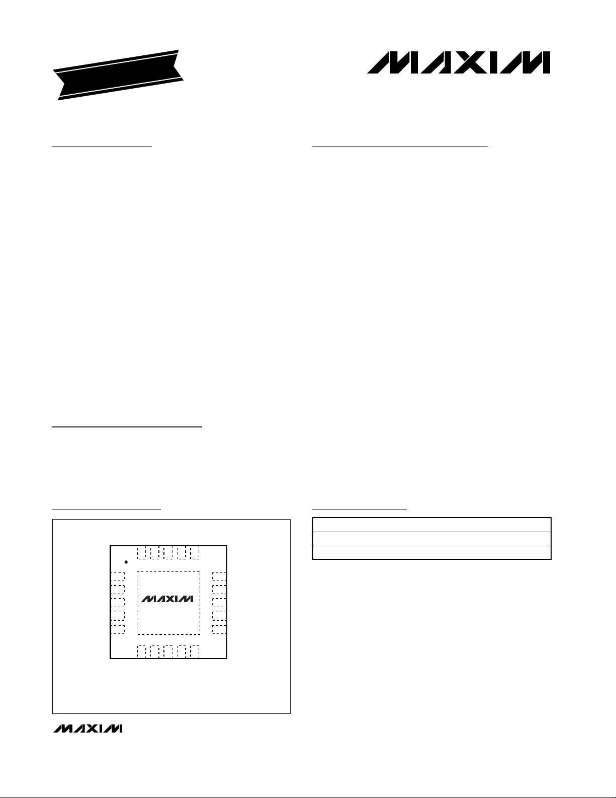
Pin Configurations
Ordering Information
19-2741; Rev 0; 4/03
For pricing, delivery, and ordering information, please contact Maxim/Dallas Direct! at
1-888-629-4642, or visit Maxim’s website at www.maxim-ic.com.
EVALUATION KIT
AVAILABLE
PART
PIN-PACKAGE
MAX1542ETP
20 Thin QFN (5mm x 5mm)
MAX1543ETP
20 Thin QFN (5mm x 5mm)
Rail-to-Rail is a registered trademark of Nippon Motorola, Ltd.
Pin Configurations continued at end of data sheet.
TOP VIEW
PGND
AGND
COM
SRC
DRN
20
1
2
I.C.
3
4
5
6
POS1
THIN QFN (5mm x 5mm)
CTL
DEL
COMP
FB
19
18
17
16
15
FREQ
14
IN
13
MAX1543
7
8
OUT1
NEG1
9
OUT2
10
NEG2
LX
12
SUP
POS2
11
TEMP RANGE
-40°C to +85°C
-40°C to +85°C
Page 2
MAX1542/MAX1543
TFT LCD DC-to-DC Converter with
Operational Amplifiers
2 _______________________________________________________________________________________
ABSOLUTE MAXIMUM RATINGS
Stresses beyond those listed under “Absolute Maximum Ratings” may cause permanent damage to the device. These are stress ratings only, and functional
operation of the device at these or any other conditions beyond those indicated in the operational sections of the specifications is not implied. Exposure to
absolute maximum rating conditions for extended periods may affect device reliability.
IN, CTL, COMP, FB, DEL, FREQ (MAX1543)
to AGND ...............................................................-0.3V to +6V
COMP, FB, DEL to AGND .............................-0.3V to (IN + 0.3V)
PGND to AGND ..................................................................±0.3V
LX to PGND ............................................................-0.3V to +14V
SUP, POS1, NEG1, OUT1, POS2,
NEG2, OUT2 to AGND .......................................-0.3V to +14V
POS1, NEG1, OUT1, POS2, NEG2,
OUT2 to AGND ......................................-0.3V to (SUP + 0.3V)
SRC, COM to AGND...............................................-0.3V to +30V
SRC to COM ...........................................................-0.3V to +30V
SRC to DRN (MAX1543).........................................-0.3V to +30V
COM to AGND ...........................................-0.3V to (SRC + 0.3V)
DRN (MAX1543) to AGND .........................-0.3V to (SRC + 0.3V)
DRN (MAX1543) to COM.........................................-30V to +30V
MAX1542 COM RMS Output Current ...............................+75mA
MAX1543 COM RMS Output Current ...............................±50mA
OUT1, OUT2 Continuous Output Current.........................±75mA
Continuous Power Dissipation (T
A
= +70°C)
20-Pin Thin QFN 5mm x 5mm
(derate 20.8mW/°C above +70°C).............................1667mW
Operating Temperature Range ...........................-40°C to +85°C
Junction Temperature .....................................................+150°C
Storage Temperature Range .............................-65°C to +150°C
Lead Temperature (soldering, 10s) .................................+300°C
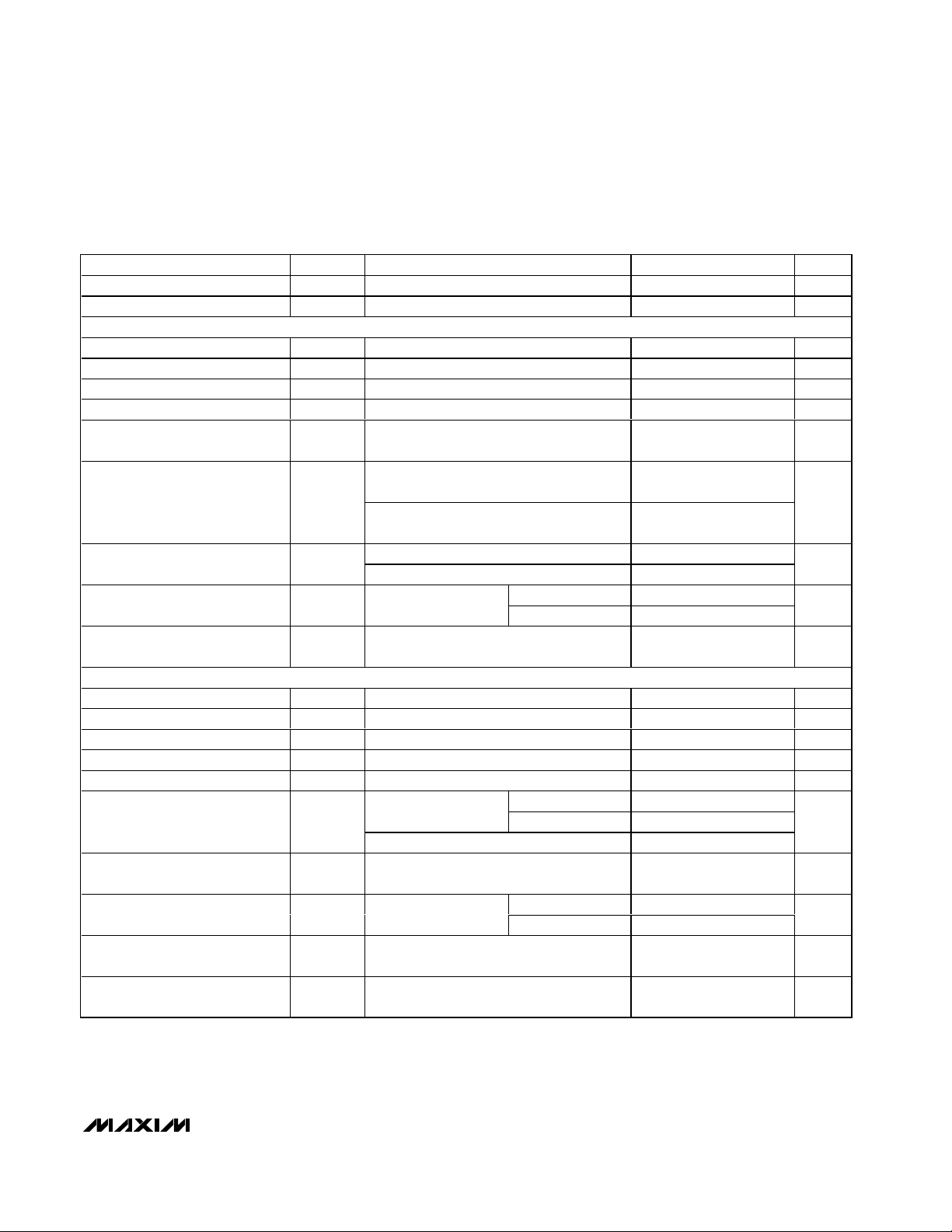
ELECTRICAL CHARACTERISTICS
(VIN= 3V, V
SUP
= 8V, V
SRC
= 28V, FREQ = IN (MAX1543), PGND = AGND = 0, TA= 0°C to +85°C, typical values at TA= +25°C,
unless otherwise noted.)
IN Supply Range V
IN Undervoltage Lockout
Threshold
IN Quiescent Current I
Duration to Trigger Fault
Condition
Thermal Shutdown
MAIN STEP-UP REGULATOR
Output Voltage Range V
Oscillator Maximum Duty Cycle 82 87 92 %
FREQ Input Low Voltage MAX1543, VIN = 2.6V to 5.5V 0.3 x V
FREQ Input High Voltage MAX1543, VIN = 2.6V to 5.5V
FREQ Pulldown Current MAX1543, V
FB Regulation Voltage V
FB Fault Trip Level VFB falling 0.96 1 1.04 V
FB Load Regulation 0 ≤ I
FB Line Regulation VIN = 2.6V to 5.5V -0.08 ±0.15 %/V
PARAMETER SYMBOL CONDITIONS MIN TYP MAX UNITS
IN
V
UVLO
MAIN
OSC
VIN rising 2.3 2.5 2.7
VIN falling 2.2 2.35 2.5
VFB = 1.3V, LX not switching 0.45 0.65
IN
VFB = 1.1V, LX switching 3.6 6.5
MAX1542 55
MAX1543
Rising edge 160
Hysteresis 15
MAX1542 1020 1200 1380
MAX1543 FREQ = AGND 512 600 768Operating Frequency f
No load
FB
≤ full load -1 %
MAIN
FREQ = AGND 51
FREQ = IN 55
FREQ = IN 1020 1200 1380
= 1.0V 3.5 5 6.5 µA
FREQ
TA = +85°C 1.224 1.240 1.256
T
= 0°C to +85°C 1.222 1.240 1.258
A
2.6 5.5 V
V
IN
0.7 x
V
IN
13 V
IN
V
mA
ms
°C
kHz
V
V
V
Page 3
MAX1542/MAX1543
TFT LCD DC-to-DC Converter with
Operational Amplifiers
_______________________________________________________________________________________ 3
ELECTRICAL CHARACTERISTICS (continued)
(VIN= 3V, V
SUP
= 8V, V
SRC
= 28V, FREQ = IN (MAX1543), PGND = AGND = 0, TA= 0°C to +85°C, typical values at TA= +25°C,
unless otherwise noted.)
)
FB Input Bias Current VFB = 1.5V -40 +40 nA
FB Transconductance ∆I
FB Voltage Gain FB to COMP 700 V/V
LX On-Resistance R
LX Leakage Current I
LX Current Limit I
Current-Sense Transresistance 0.30 0.50 0.65 Ω
Soft-Start Step Size I
OPERATIONAL AMPLIFIERS
SUP Supply Range V
SUP Supply Current I
Input Offset Voltage V
Input Bias Current I
Input Common-Mode Voltage
Range
Common-Mode Rejection Ratio CMRR 0 ≤ V
Open-Loop Gain 125 dB
Output Voltage Swing High V
Output Voltage Swing Low V
Short-Circuit Current To V
Output Source-and-Sink Current
Power-Supply Rejection Ratio PSRR
Slew Rate 7.5 V/µs
PARAMETER SYMBOL CONDITIONS MIN TYP MAX UNITS
= 5µA 75 160 280 µS
COMP
LX(ON
LX
LIM
VLX = 13V 0.01 20 µA
VFB = 1V, duty cycle = 65% 1.2 1.5 1.8 A
210 400 mΩ
MAX1542 14
SS
SUP
SUP
OS
BIAS
V
CM
OH
OL
MAX1543
Buffer configuration, V
VCM = V
/2, TA = +25°C 0 12 mV
SUP
NEG1, NEG2, POS1, POS2 +1 ±50 nA
, V
NEG_
POS_
I
= 100µA
OUT_
I
= 5mA
OUT_
I
= -100µA 2 15
OUT_
I
= -5mA 80 150
OUT_
/2
SUP
Buffer configuration, V
|∆V
< 10mV
OS|
DC, 6V ≤ V
/2
V
SUP
SUP
≤ 13V, V
FREQ = AGND 13Soft-Start Period t
FREQ = IN 14
= 4V, no load 1.3 1.9 mA
POS_
≤ V
SUP
V
V
Source 50 150
Sink 50 140
= 4V,
POS_
, V
POS_
=
NEG_
/ 8 A
LIM
4.5 13.0 V
0V
SUP
50 90 dB
SUP
-15V
SUP
-
2
-
V
SUP
150
SUP
80
-
40 mA
60 100 dB
ms
V
mV
mV
mA
-3dB Bandwidth RL = 10kΩ, CL =10pF, buffer configuration 12 MHz
Gain-Bandwidth Product GBW Buffer configuration 8 MHz
POSITIVE GATE-DRIVER TIMING AND CONTROL SWITCHES
DEL Capacitor Charge Current During startup, V
= 1V 4 5 6 µA
DEL
Page 4
MAX1542/MAX1543
TFT LCD DC-to-DC Converter with
Operational Amplifiers
4 _______________________________________________________________________________________
ELECTRICAL CHARACTERISTICS
(VIN= 3V, V
SUP
= 8V, V
SRC
= 28V, FREQ = IN (MAX1543), PGND = AGND = 0, TA= -40°C to +85°C, unless otherwise noted.)
PARAMETER
CONDITIONS
UNITS
DEL Turn-On Threshold
)
V
DEL Discharge Switch OnResistance
During UVLO, V
IN
= 2.2V 20 Ω
CTL Input Low Voltage VIN = 2.6V to 5.5V 0.6 V
CTL Input High Voltage VIN = 2.6V to 5.5V 2 V
CTL Input Leakage Current CTL = AGND or IN -1 +1 µA
CTL-to-SRC Propagation Delay
ns
SRC Input Voltage Range 28 V
MAX1542 70
V
D RN
= 8V , C TL = IN ,
V
D E L
= 1.5V
MAX1543
SRC Input Current I
SRC
V
DRN
= 8V, CTL = AGND, V
DEL
= 1.5V 15 30
µA
DRN Input Current I
DRC
V
DRN
= 8V, CTL = AGND, V
DEL
= 1.5V,
MAX1543
90
µA
MAX1542 5 10
SRC to COM Switch OnResistance
)
V
DEL
= 1.5V,
CTL = IN
MAX1543 15 30
Ω
DRN to COM Switch OnResistance (MAX1543)
)
V
DEL
= 1.5V, CTL = AGND 30 60 Ω
COM to PGND Switch OnResistance (MAX1543)
)
V
DEL
= 1.1V
Ω
PARAMETER
SYMBOL
CONDITIONS
MIN
TYP
MAX
UNITS
IN Supply Range V
IN
2.6 5.5 V
VIN rising 2.3 2.7
IN Undervoltage Lockout
Threshold
V
UVLO
VIN falling 2.2 2.5
V
V
FB
= 1.3V, LX not switching
IN Quiescent Current I
IN
V
FB
= 1.1V, LX switching 6.5
mA
MAIN STEP-UP REGULATOR
Output Voltage Range V
MAIN
V
IN
13 V
MAX1542
FREQ = AGND
Operating Frequency f
OSC
MAX1543
FREQ = IN
kHz
FB Regulation Voltage V
FB
No load
V
FB Fault Trip Level VFB falling
V
FB Line Regulation VIN = 2.6V to 5.5V
%/V
FB Transconductance ∆I
COMP
= 5µA 75
µS
LX On-Resistance
)
mΩ
ELECTRICAL CHARACTERISTICS (continued)
(VIN= 3V, V
SUP
= 8V, V
SRC
= 28V, FREQ = IN (MAX1543), PGND = AGND = 0, TA= 0°C to +85°C, typical values at TA= +25°C,
unless otherwise noted.)
SYMBOL
V
TH(DEL
MIN TYP MAX
1.178 1.240 1.302
100
130
100 180
R
SRC(ON
R
DRN(ON
R
COM(ON
R
LX(ON
350 1000 1800
1000 1400
512 768
1000 1400
1.215 1.260
0.96 1.04
150
0.65
0.15
300
400
Page 5
MAX1542/MAX1543
TFT LCD DC-to-DC Converter with
Operational Amplifiers
_______________________________________________________________________________________ 5
)
)
)
)
ELECTRICAL CHARACTERISTICS (continued)
(VIN= 3V, V
SUP
= 8V, V
SRC
= 28V, FREQ = IN (MAX1543), PGND = AGND = 0, TA= -40°C to +85°C, unless otherwise noted.)
LX Current Limit I
Current-Sense Transresistance 0.30 0.65 Ω
OPERATIONAL AMPLIFIERS
SUP Supply Range V
SUP Supply Current I
Input Offset Voltage V
Input Bias Current I
Input Common-Mode Voltage
Range
Output Voltage Swing High V
Output Voltage Swing Low V
Short-Circuit Current To V
Output Source-and-Sink Current
POSITIVE GATE-DRIVER TIMING AND CONTROL SWITCHES
DEL Capacitor Charge Current During startup, V
DEL Turn-On Threshold V
CTL Input Low Voltage VIN = 2.6V to 5.5V 0.6 V
CTL Input High Voltage VIN = 2.6V to 5.5V 2 V
SRC Input Voltage Range 28 V
SRC Input Current I
DRN Input Current I
SRC to COM Switch OnResistance
DRN to COM Switch OnResistance (MAX1543)
COM to PGND Switch OnResistance (MAX1543)
PARAMETER SYMBOL CONDITIONS MIN TYP MAX UNITS
LIM
SUP
SUP
OS
BIAS
V
CM
OH
TH (DEL
SRC
DRN
R
SRC(ON
R
DRN(ON
R
COM(ON
VFB = 1V, duty cycle = 65% 1.2 1.8 A
4.5 13.0 V
Buffer configuration, V
VCM = V
/2, TA = +25ºC12mV
SUP
= 4V, no load 2.1 mA
POS_
NEG1, NEG2, POS1, POS2 ±50 nA
0V
V
-
I
OUT_
I
OUT_
I
OL
OUT_
I
OUT_
Buffer configuration, V
| ∆V
OS
= 100µA
= 5mA
= -100µA 15
= -5mA 150
SUP
/2
Source 50
Sink 50
= 4V,
POS_
| < 10mV
= 1.0V 4 6 µA
DEL
SUP
15
V
-
SUP
150
40 mA
1.178 1.302 V
V
= 8V, CTL = IN,
DRN
= 1.5V
V
DEL
V
= 8V, CTL = AGND, V
DRN
V
= 8V, CTL = AGND, V
DRN
MAX1542 130
MAX1543 180
= 1.5V 30
DEL
= 1.5V,
DEL
MAX1543
V
= 1.5V, CTL = IN
DEL
V
= 1.5V, CTL = AGND 60 Ω
DEL
V
= 1.1V 350 1800 Ω
DEL
MAX1542 10
MAX1543 30
SUP
150 µA
V
mV
mV
mA
µA
Ω
Page 6
MAX1542/MAX1543
TFT LCD DC-to-DC Converter with
Operational Amplifiers
6 _______________________________________________________________________________________
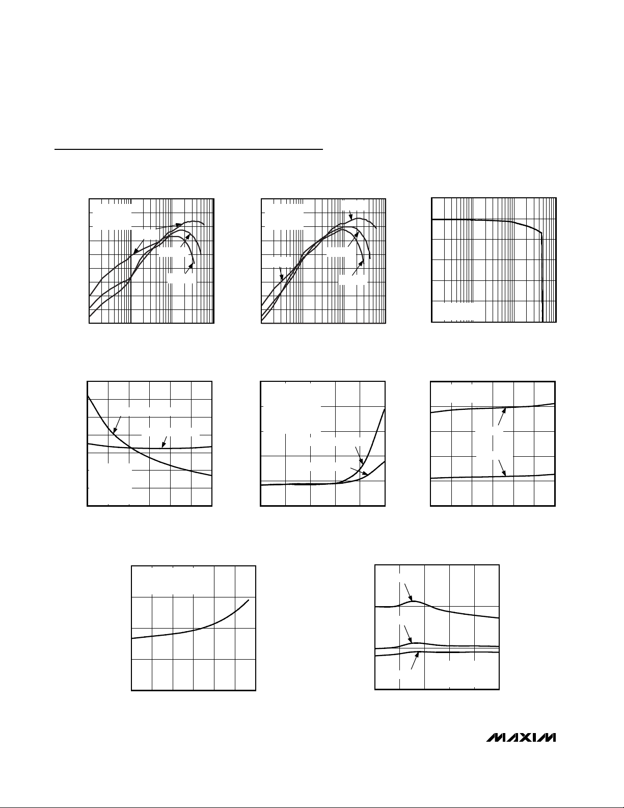
Typical Operating Characteristics
(VIN= 3.3V, V
MAIN
= 8V, f
OSC
= 1.2MHz, TA= +25°C, unless otherwise noted.)
50
1 1000100
STEP-UP REGULATOR EFFICIENCY
vs. LOAD CURRENT (V
MAIN
= 8V)
65
55
85
75
95
70
60
90
80
MAX1542 toc01
LOAD CURRENT (mA)
EFFICIENCY (%)
10
MAX1543
f
OSC
= 1.2MHz
L = 4.7µH
VIN = 3.3V
VIN = 2.7V
VIN = 5V
50
1 100010010
STEP-UP REGULATOR EFFICIENCY
vs. LOAD CURRENT (V
MAIN
= 8V)
65
55
85
75
95
70
60
90
80
MAX1542 toc02
LOAD CURRENT (mA)
EFFICIENCY (%)
MAX1543
f
OSC
= 640kHz
L = 10µH
VIN = 3.3V
VIN = 2.7V
VIN = 5V
VIN = 5V
STEP-UP REGULATOR OUTPUT VOLTAGE
vs. LOAD CURRENT (V
MAIN
= 8V)
MAX1542 toc03
LOAD CURRENT (mA)
OUTPUT VOLTAGE (V)
10 100
7.6
7.7
7.8
7.9
8.0
8.1
7.5
1 1000
VIN = 3.3V
f
OSC
= 1.2MHz
MAX1542 toc04
VIN (V)
SUPPLY CURRENT (mA)
5.04.54.03.53.0
0.1
0.2
0.3
0.4
0.5
0.6
0.7
0
2.5 5.5
STEP-UP REGULATOR SUPPLY CURRENT
vs. SUPPLY VOLTAGE
NO LOAD
f
OSC
= 1.2MHz
R
1
= 75kΩ
R
2
= 13.7kΩ
SUP DISCONNECTED
CURRENT INTO INDUCTOR
CURRENT INTO IN PIN
STEP-UP REGULATOR SUPPLY CURRENT
vs. TEMPERATURE
MAX1542 toc05
TEMPERATURE (°C)
SUPPLY CURRENT (mA)
603510-15
0.4
0.8
1.2
1.6
2.0
0
-40 85
NO LOAD
V
IN
= 3.3V
f
OSC
= 1.2MHz
R
1
= 75kΩ
R
2
= 13.7kΩ
SUP DISCONNECTED
CURRENT INTO INDUCTOR
CURRENT INTO IN PIN
MAX1542 toc06
VIN (V)
SWITCHING FREQUENCY (kHz)
5.04.54.03.53.0
600
800
1000
1200
1400
400
2.5 5.5
SWITCHING FREQUENCY
vs. INPUT VOLTAGE
MAX1543
I
MAIN
= 200mA
FREQ = IN
FREQ = AGND
SUP SUPPLY CURRENT
vs. SUP VOLTAGE
MAX1542 toc07
V
SUP
(V)
I
SUP
(mA)
12.010.59.07.56.0
1.00
1.25
1.50
1.75
0.75
4.5 13.5
NO LOAD
BUFFER CONFIGURATION
POS_ = V
SUP
/2
SUP SUPPLY CURRENT
vs. TEMPERATURE
MAX1542 toc08
TEMPERATURE (°C)
I
SUP
(mA)
603510-15
1.2
1.6
2.0
0.8
-40 85
NO LOAD
BUFFER CONFIGURATION
V
POS
= V
SUP
/2
V
SUP
= 13V
V
SUP
= 8V
V
SUP
= 5V
Page 7
MAX1542/MAX1543
TFT LCD DC-to-DC Converter with
Operational Amplifiers
_______________________________________________________________________________________ 7
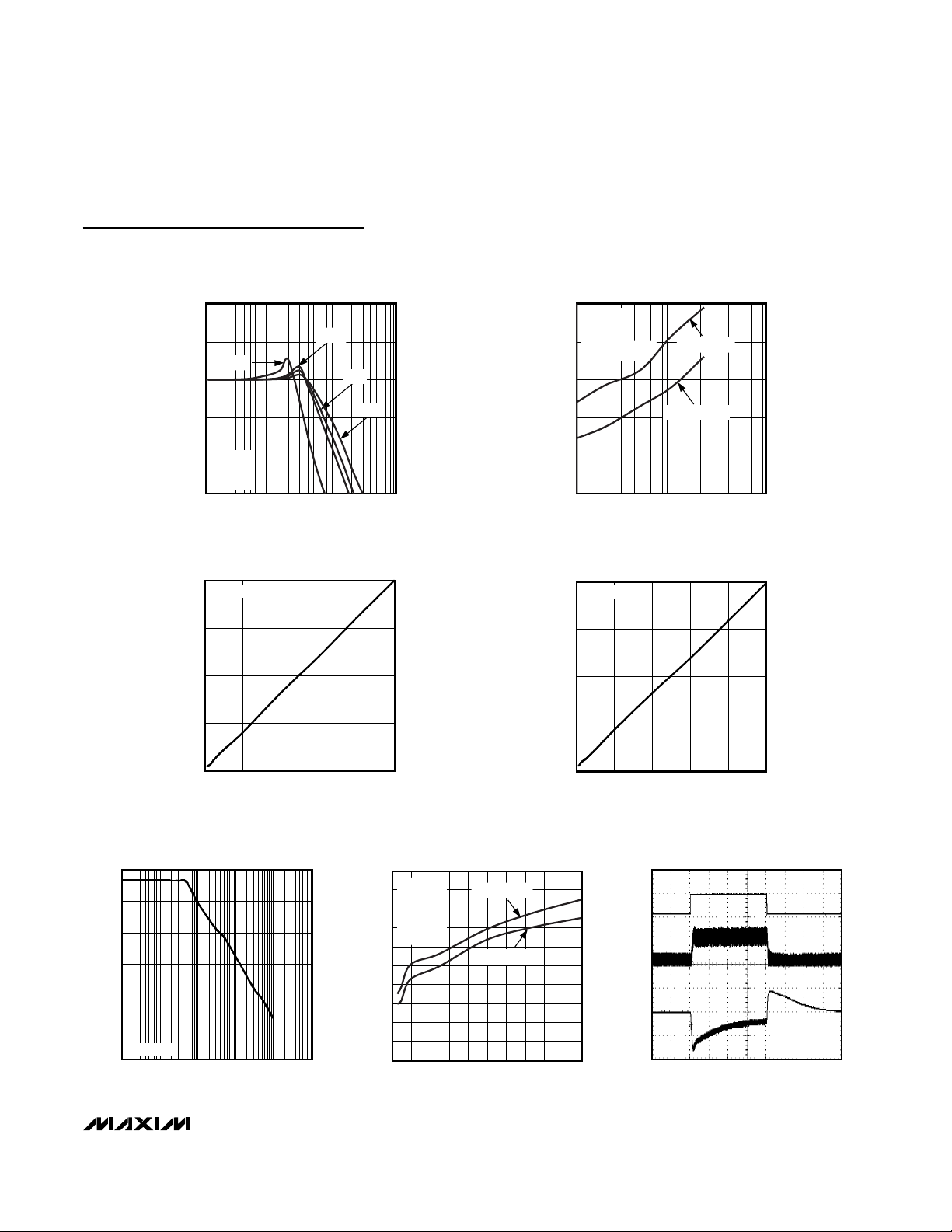
Typical Operating Characteristics (continued)
(VIN= 3.3V, V
MAIN
= 8V, f
OSC
= 1.2MHz, TA= +25°C, unless otherwise noted.)
OPERATIONAL AMPLIFIER
OUTPUT LOW VOLTAGE vs. LOAD
MAX1542 toc12
I
OUT_
(mA)
V
OL
(mV)
8642
40
80
120
160
0
010
V
SUP
= 8V
A
V
= 1
OPERATIONAL AMPLIFIER
OUTPUT HIGH VOLTAGE vs. LOAD
MAX1542 toc11
I
OUT_
(mA)
V
SUP
- V
OUT
(mV)
8642
40
80
120
160
0
010
V
SUP
= 8V
A
V
= 1
POWER-SUPPLY REJECTION RATIO
vs. FREQUENCY
MAX1542 toc13
FREQUENCY (Hz)
PSRR (dB)
1k100101
20
40
60
80
100
120
0
0.1 10k
V
SUP
= 8V
OPERATIONAL AMPLIFIER
SETTLING TIME vs. STEP SIZE
MAX1542 toc14
STEP SIZE (V)
SETTLING TIME (ns)
1.4 1.6 1.81.0 1.20.4 0.6 0.80.2
100
50
200
150
300
250
400
450
350
500
0
0 2.0
V
SUP
= 8V
A
V
= +1
R
L
= 10kΩ
C
L
= 10pF
V
CM
= 4V
RISING EDGE
FALLING EDGE
STEP-UP REGULATOR
LOAD-TRANSIENT RESPONSE
MAX1542 toc15
40µs/div
I
MAIN
200mA/div
I
L
500mA/div
200mA
20mA
V
MAIN
AC-COUPLED
100mV/div
L = 4.7µH
R
COMP
= 120kΩ
C
COMP
= 470pF
OPERATIONAL AMPLIFIER FREQUENCY
RESPONSE FOR VARIOUS C
20
10
1000pF
0
-10
MAGNITUDE (dB)
-20
V
= 8V
SUP
= 1
A
V
= 10kΩ
R
L
-30
100 100k10k1k
FREQUENCY (Hz)
OPERATIONAL AMPLIFIER OVERSHOOT
vs. LOAD CAPACITANCE
V
= 8V
SUP
= 10kΩ
R
L
= 1
A
V
POS_ = 4V ±50mV
1 100 1000
LOAD CAPACITANCE (pF)
RISING EDGE
FALLING EDGE
100pF
56pF
LOAD
15pF
MAX1542 toc09
100
80
60
40
OVERSHOOT (%)
20
0
MAX1542 toc10
Page 8
MAX1542/MAX1543
TFT LCD DC-to-DC Converter with
Operational Amplifiers
8 _______________________________________________________________________________________
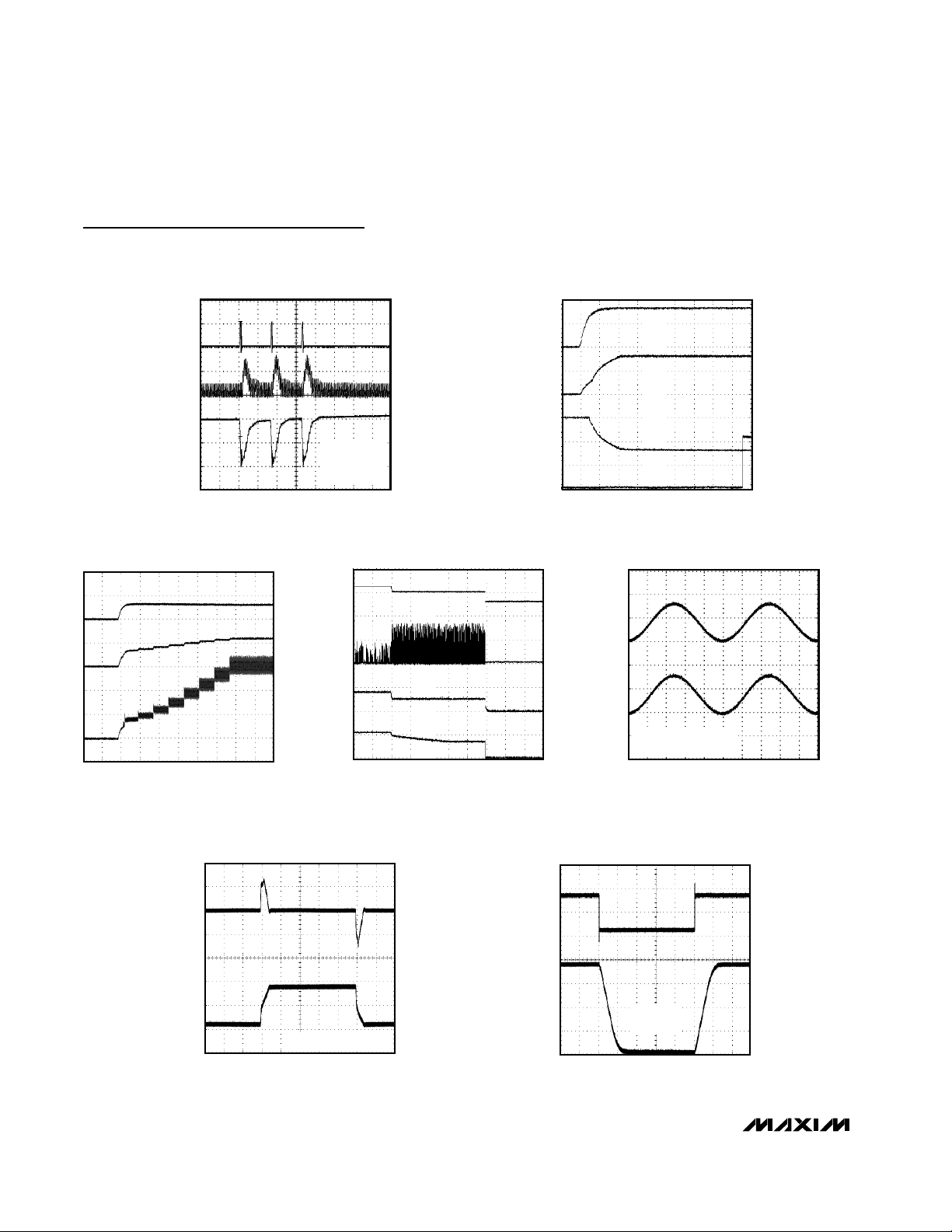
Typical Operating Characteristics (continued)
(VIN= 3.3V, V
MAIN
= 8V, f
OSC
= 1.2MHz, TA= +25°C, unless otherwise noted.)
STEP-UP REGULATOR
PULSED LOAD-TRANSIENT RESPONSE
MAX1542 toc16
10µs/div
I
MAIN
1A/div
I
L
500mA/div
V
MAIN
100mV/div
AC-COUPLED
L = 4.7µH
R
COMP
= 120kΩ
C
COMP
= 470pF
STARTUP SEQUENCE
MAX1542 toc17
1ms/div
V
IN
2V/div
V
MAIN
8V/div
V
GOFF
5V/div
V
COM
10V/div
HEAVY-LOAD
SOFT-START WAVEFORMS
MAX1542 toc18
2ms/div
R
LOAD
= 10Ω
V
IN
5V/div
V
MAIN
5V/div
I
L
500mA/div
TIMER DELAY LATCH
RESPONSE TO OVERLOAD
MAX1542 toc19
10ms/div
I
L
2A/div
V
MAIN
5V/div
V
OUT1
5V/div
V
COM
20V/div
OPERATIONAL AMPLIFIER
RAIL-TO-RAIL I/O PERFORMANCE
MAX1542 toc20
100µs/div
V
POS1
5V/div
V
OUT1
5V/div
V
SUP
= 8V
BUFFER CONFIGURATION
OPERATIONAL AMPLIFIER
LOAD-TRANSIENT RESPONSE
MAX1542 toc21
1µs/div
V
OUT1
1V/div
AC-COUPLED
4V
+50
0
-50
I
OUT1
50mA/div
BUFFER CONFIGURATION
OPERATIONAL AMPLIFIER
LARGE-SIGNAL STEP RESPONSE
MAX1542 toc22
1µs/div
V
POS1
500mV/div
AC-COUPLED
4V
V
OUT1
2V/div
V
SUP
= 8V
A
V
= 10
Page 9
MAX1542/MAX1543
TFT LCD DC-to-DC Converter with
Operational Amplifiers
_______________________________________________________________________________________ 9
Typical Operating Characteristics (continued)
(VIN= 3.3V, V
MAIN
= 8V, f
OSC
= 1.2MHz, TA= +25°C, unless otherwise noted.)
OPERATIONAL AMPLIFIER
SMALL-SIGNAL STEP RESPONSE
MAX1542 toc24
200ns/div
POS_
50mV/div
AC-COUPLED
OUT_
50mV/div
AC-COUPLED
V
SUP
= 8V, AV = 1
CH2 + OVER
6.234%
CH2 - OVER
2.352%
OPERATIONAL AMPLIFIER
LARGE-SIGNAL STEP RESPONSE
MAX1542 toc23
1µs/div
V
OUT_
1V/div
CHI AMPL
4.86V
CHI + OVER
4.970%
AV = 1
Pin Description
MAX1542 MAX1543
1 1 COM
2 2 SRC
3, 15, 20 — N.C. No Connection. Not internally connected.
— 3 I.C. Internal Connection. Make no connection to this pin.
4 4 PGND
5 5 AGND Analog Ground. Connect to power ground (PGND) underneath the IC.
6 6 POS1 Operational Amplifier 1 Noninverting Input
7 7 NEG1 Operational Amplifier 1 Inverting Input
8 8 OUT1 Operational Amplifier 1 Output
9 9 OUT2 Operational Amplifier 2 Output
10 10 NEG2 Operational Amplifier 2 Inverting Input
11 11 POS2 Operational Amplifier 2 Noninverting Input
12 12 SUP
13 13 LX
PIN
NAME FUNCTION
Internal High-Voltage MOSFET Switch Common Terminal. Do not allow the voltage on
COM to exceed V
SRC
.
Switch Input. Source of the internal high-voltage P-channel MOSFET. Bypass SRC to
PGND with a minimum of 0.1µF close to the pins.
Power Ground. PGND is the source of the main boost N-channel power MOSFET. Connect
PGND to the output capacitor ground terminals through a short, wide PC board trace.
Connect to analog ground (AGND) underneath the IC.
Operational Amplifier Power Input. Positive supply rail for the OUT1 and OUT2 amplifiers.
Typically connected to V
MAIN
Power MOSFET N-Channel Drain and Switching Node. Connect the inductor and catch
diode to LX and minimize the trace area for lowest EMI.
. Bypass SUP to AGND with a 0.1µF capacitor.
Page 10
MAX1542/MAX1543
TFT LCD DC-to-DC Converter with
Operational Amplifiers
10 ______________________________________________________________________________________
Pin Description (continued)
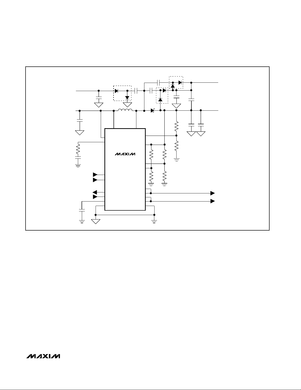
Typical Application Circuits
The MAX1542 typical application circuit (Figure 1) and
the MAX1543 typical application circuit (Figure 2) generate an +8V source driver supply and approximately
+22V and -7V gate driver supplies for TFT displays. The
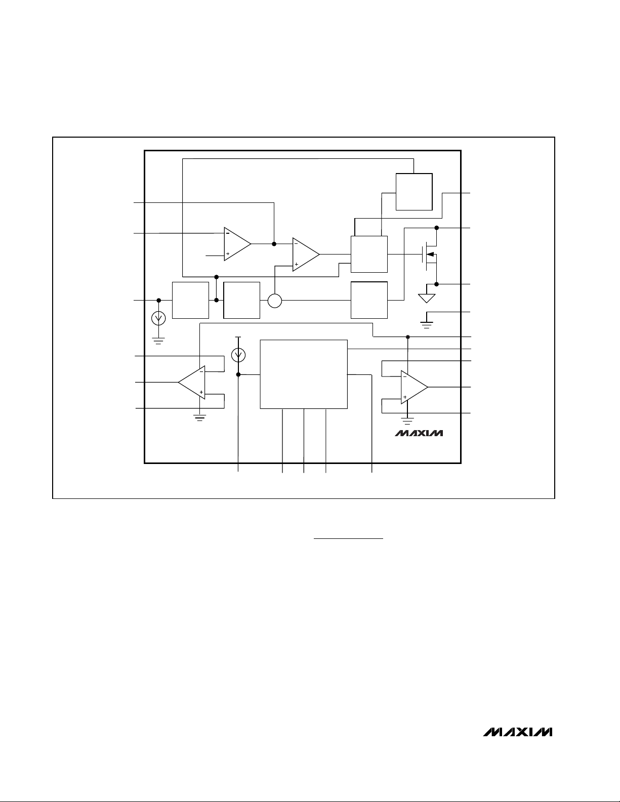
input voltage is from +2.6V to +5.5V. Table 1 lists recommended components and Table 2 lists contact information for component suppliers.
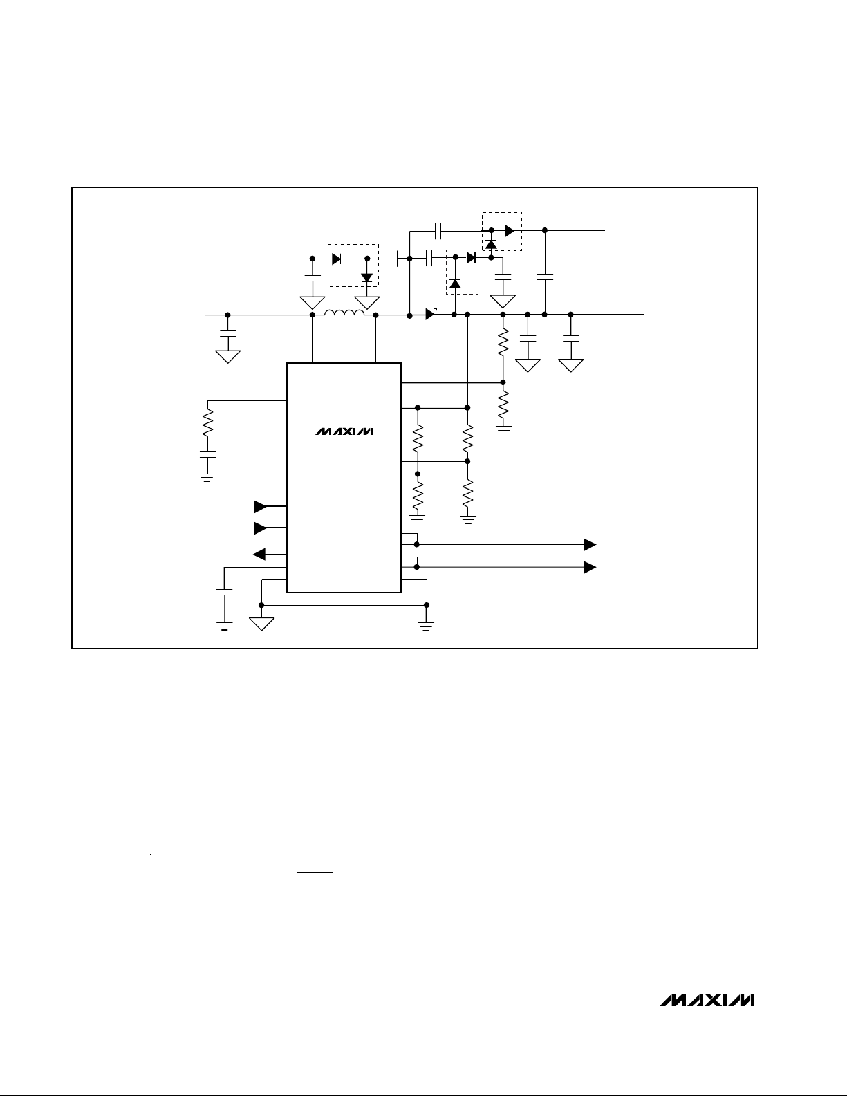
Detailed Description
The MAX1542/MAX1543 include a high-performance
step-up regulator, two high-current operational amplifiers, and startup timing and level-shifting functionality
useful for active matrix TFT LCDs. Figure 3 shows the
MAX1542/MAX1543 functional diagram.
Main Step-Up Converter
The MAX1542/MAX1543 main step-up converter
switches at 1.2MHz or 640kHz (MAX1543 only) (see the
Oscillator Frequency (FREQ) section). The devices
employ a current-mode, fixed-frequency, pulse-width
modulation (PWM) architecture to maximize loop bandwidth providing fast transient response to pulsed loads
found in source drivers for TFT LCD panels. The highswitching frequency also allows the use of low-profile
inductors and capacitors to minimize the thickness of
LCD panel designs. The integrated high-efficiency
MOSFET and the IC’s built-in digital soft-start function
reduce the number of external components required
while controlling inrush current. The output voltage of
the main step-up converter (V
MAIN
) can be set from V
IN
to 13V with an external resistive voltage-divider at FB.
PIN
MAX1542 MAX1543
14 14 IN Supply Voltage. IN can range from 2.6V to 5.5V.
— 15 FREQ
16 16 FB
17 17 COMP
18 18 DEL
19 19 CTL
— 20 DRN
NAME FUNCTION
Oscillator Frequency Select Input. Pull FREQ low or leave it unconnected for 640kHz
operation. Connect FREQ high for 1.2MHz operation. This input has a 5µA pulldown
current.
Step-Up Converter Feedback Input. Regulates to 1.24V (nominal). Connect a resistordivider from the output (V
within 5mm of FB.
Step-Up Regulator Error Amplifier Compensation Point. Connect a series RC from COMP
to AGND. See the Loop Compensation section for component selection guidelines.
High-Voltage Switch Delay Input. Connect a capacitor from DEL to AGND to set the highvoltage switch startup delay. A 5µA current source charges C
For the MAX1542, the high-voltage switch between SRC and COM is disabled until V
exceeds 1.24V. Following the delay period, CTL controls the state of the high-voltage
switch.
For the MAX1543, the switches between SRC, COM, and DRN are disabled and a 1kΩ
pulldown between COM and PGND is enabled until V
delay period, the 1kΩ pulldown is released and CTL controls the state of the high-voltage
switches (see the Delay Control Circuit section).
High-Voltage Switch Control Input. When CTL is high, the high-voltage switch between
COM and SRC is on and the high-voltage switches between COM and DRN (MAX1543)
are off. When CTL is low, the high-voltage switch between COM and SRC is off and the
high-voltage switches between COM and DRN (MAX1543) are on. CTL is inhibited by the
undervoltage lockout and when V
Switch Input. Drain of the internal high-voltage back-to-back P-channel MOSFETs
connected to COM.
) to FB to analog ground (AGND). Place the resistor-divider
MAIN
.
DEL
exceeds 1.24V. Following the
DEL
is less than 1.24V.
DEL
DEL
Page 11
MAX1542/MAX1543
TFT LCD DC-to-DC Converter with
Operational Amplifiers
______________________________________________________________________________________ 11
The regulator controls the output voltage and the power
delivered to the outputs by modulating the duty cycle
(D) of the power MOSFET in each switching cycle. The
duty cycle of the MOSFET is approximated by:
The device regulates the output voltage through a combination of an error amplifier, two comparators, and
several signal generators (Figure 3). The error amplifier
compares the signal at FB to 1.24V and varies the
COMP output. The voltage at COMP determines the
current trip point each time the internal MOSFET turns
on. As the load varies, the error amplifier sources or
sinks current to the COMP output accordingly to produce the inductor peak current necessary to service
the load. To maintain stability at high duty cycles, a
slope compensation signal is summed with the currentsense signal.
Operational Amplifiers
The MAX1542/MAX1543 include two operational amplifiers that are typically used to drive the LCD backplane
VCOM and/or the gamma correction divider string. The
operational amplifiers feature ±150mA output short-circuit current, 7.5V/µs slew rate, and 12MHz bandwidth.
The rail-to-rail inputs and outputs maximize flexibility.
Short-Circuit Current Limit
The MAX1542/MAX1543 operational amplifiers limit
short-circuit current to ±150mA if the output is directly
shorted to SUP or AGND. In such a condition, the junction temperature of the IC rises until it reaches the thermal shutdown threshold, typically +160°C. Once it
reaches this threshold, the IC shuts down and remains
inactive until IN falls below V
UVLO
.
Driving Pure Capacitive Loads
The operational amplifiers are typically used to drive
the LCD backplane (VCOM) or the gamma correction
divider string. The LCD backplane consists of a distributed series capacitance and resistance, a load easily
driven by the operational amplifiers. However, if the
operational amplifiers are used in an application with a
pure capacitive load, steps must be taken to ensure
stable operation.
As the operational amplifier’s capacitive load increases,
the amplifier bandwidth decreases and gain peaking
increases. A small 5Ω to 50Ω resistance placed between
OUT_ and the capacitive load reduces peaking but
reduces the amplifier gain. An alternative method of
reducing peaking is the use of a snubber circuit. A 150Ω
and 10nF (typ) shunt load, or snubber, does not continuously load the output or reduce amplifier gain.
D
VV
V
MAIN IN
MAIN
≈
−
Table 1. Component List
Table 2. Component Suppliers
DESIGNATION DESCRIPTION PART
C1 10µF ±10%, 6.3V X5R ceramic capacitor TDK C3216X5R0J106K
C8, C9 4.7µF ±10%, 10V X5R ceramic capacitors TDK C3225X5R1A475K
D1 1A, 30V Schottky diode Toshiba CRS02
D2, D3, D4 200mA, 100V dual ultra-fast diodes Fairchild MMBD4148SE
L1 4.7µH, 1.3A inductor Sumida CLS5D11HP-4R7
Inductors
Sumida USA 847-956-0666 847-956-0702 www.sumida.com
Capacitors
TDK 847-803-6100 847-803-6296 www.component.tdk.com
Diodes
Fairchild 888-522-5372 408-822-2104 www.fairchildsemi.com
Toshiba 949-455-2000 949-859-3963 www.toshiba.com/taec/
SUPPLIER PHONE FAX WEBSITE
Page 12
MAX1542/MAX1543
TFT LCD DC-to-DC Converter with
Operational Amplifiers
12 ______________________________________________________________________________________
Delay Control Circuit
A capacitor from DEL to AGND selects the switch control
block supply startup delay. After the input voltage
exceeds V
UVLO
, a 5µA current source charges C
DEL
.
Once the capacitor voltage exceeds the turn-on threshold (1.24V) COM can be connected to SRC, depending
on the state of CTL. Before startup and when IN is less
than V
UVLO
, DEL is internally connected to AGND to dis-
charge C
DEL
. Select C
DEL
using the following equation:
MAX1542 Control Block Switch
The switch control input (CTL) is not activated until
V
DEL
exceeds the turn-on voltage (1.24V) and the input
voltage (VIN) exceeds V
UVLO
(2.5V). Once activated,
CTL controls the P-channel MOSFET, between COM
and SRC. A high at CTL turns on Q1 between SRC and
COM, and a low at CTL turns Q1 off (Figure 4).
MAX1543 Control Block Switch
The switch control input (CTL) is not activated until the
input voltage (VIN) exceeds V
UVLO
(2.5V) and V
DEL
exceeds the turn-on voltage (1.24V). During UVLO or
when DEL is below the turn-on threshold, COM is
pulled low to PGND through Q3 and a 1kΩ resistance.
Once activated, CTL controls the COM MOSFETs,
switching COM between SRC and DRN. A high at CTL
turns on Q1 and disables Q2. A low at CTL turns on Q2
and turns off Q1 (Figure 4).
Undervoltage Lockout (UVLO)
The UVLO comparator of the MAX1542/MAX1543 compares the input voltage at IN with the UVLO threshold
C DELAY TIME
A
V
DEL
=×()
.5124
µ
Figure 1. MAX1542 Typical Application Circuit
C4
0.1µF
C3
G_OFF
-7V AT 20mA
V
IN
2.6V TO 5.5V
C1
10µF
R8
100kΩ
C11
220pF
0.1µF
C2
COMP
SRC
CTL
COM
DEL
C10
33nF
PGND
L1
4.7µF
MAX1542
0.1µF
D2
LXIN
SUP
POS1
POS2
NEG1
OUT1
NEG2
OUT2
AGND
C5
0.1µF
FB
D1
R5
40kΩ
R6
40kΩ
D3
R1
75kΩ
R3
40kΩ
R4
40kΩ
D4
C6
0.1µF
R2
13.7kΩ
+22V AT 20mA
C7
0.1µF
C8
4.7µF
G_ON
C9
4.7µF
BACKPLANE
V
MAIN
+8V AT 250mA
TO VCOM
Page 13
MAX1542/MAX1543
TFT LCD DC-to-DC Converter with
Operational Amplifiers
______________________________________________________________________________________ 13
(2.5V rising, 2.35V falling, typ) to ensure that the input
voltage is high enough for reliable operation. The
150mV (typ) hysteresis prevents supply transients from
causing a restart. Once the input voltage exceeds the
UVLO threshold, startup begins. When the input voltage falls below the UVLO threshold, the controller turns
off the N-channel MOSFET, the switch control block
turns off Q1, and the operational amplifier outputs float.
For the MAX1543, the switch control block also turns off
Q2 and turns on Q3 when the input voltage falls below
the UVLO threshold (Figure 4).
Oscillator Frequency (FREQ)
The MAX1542 internal oscillator is preset to 1.2MHz. The
internal oscillator frequency is pin programmable for the
MAX1543. Connect FREQ to ground or leave it unconnected for 640kHz operation and connect it to VINfor
1.2MHz operation. FREQ has a 5µA (typ) pulldown current.
Fault Protection
Once the soft-start routine is complete, if the output of
the main regulator is below the fault detection threshold,
the MAX1542/MAX1543 activate the fault timer. If the
fault condition continuously exists throughout the fault
timer duration, the MAX1542/MAX1543 set the fault
latch, which shuts down the device. After removing the
fault condition, cycle the input voltage (IN) below V
UVLO
to clear the fault latch and reactivate the device.
Digital Soft-Start
The MAX1542/MAX1543 digital soft-start period duration is 14ms (typ). During this time, the MAX1542/
MAX1543 directly limit the peak inductor current, allowing from zero up to the full current-limit value in eight
equal current steps (I
LIM
/8). The maximum load current
is available after output voltage reaches the full regulation threshold (which terminates soft-start), or after the
soft-start timer expires.
Figure 2. MAX1543 Typical Application Circuit
2.6V TO 5.5V
C1
10µF
C11
220pF
G_OFF
-7V AT 20mA
V
IN
R8
100kΩ
C10
33nF
C2
0.1µF
FREQ
COMP
CTL
SRC
COM
DRN
DEL
PGND
D2
L1
4.7µF
MAX1543
C3
0.1µF
LXIN
SUP
POS1
POS2
NEG1
OUT1
NEG2
OUT2
AGND
FB
C4
0.1µF
C5
0.1µF
D1
R5
40kΩ
R6
40kΩR440kΩ
D4
C6
75kΩ
R3
40kΩ
0.1µF
C8
R1
4.7µF
R2
13.7kΩ
D3
G_ON
+22V AT 20mA
C7
0.1µF
+8V AT 250mA
C9
4.7µF
TO VCOM
BACKPLANE
V
MAIN
Page 14
MAX1542/MAX1543
TFT LCD DC-to-DC Converter with
Operational Amplifiers
14 ______________________________________________________________________________________
Thermal-Overload Protection
Thermal-overload protection prevents excessive power
dissipation from overheating the MAX1542/MAX1543.
When the junction temperature exceeds TJ= +160°C, a
thermal sensor immediately activates the fault protection, which shuts down the device, allowing the IC to
cool. The input voltage must fall (below V
UVLO
) to clear
the fault latch and reactivate the controller.
Thermal-overload protection protects the controller in
the event of fault conditions. For continuous operation,
do not exceed the absolute maximum junction-temperature rating of T
J
= +150°C.
Applications Information
Inductor Selection
The primary considerations in inductor selection are
inductor physical shape, circuit efficiency, and cost.
The factors that determine the inductance value are
input voltage, output voltage, switching frequency, and
maximum output current. Final inductor selection
includes ensuring the chosen inductor meets the application’s peak current and RMS current requirements.
Very high inductance values minimize the current ripple
and therefore reduce the peak current, which decreases core losses in the inductor and I2R losses in the circuit’s entire power path. However, large inductance
Figure 3. Functional Diagram
COMP
FB
1.24V
FREQ*
NEG1
OUT1
POS1
*MAX1543 ONLY.
OSCILLATOR
5µA
ERROR
AMPLIFIER
SLOPE
COMPEN-
SATION
ERROR
COMPARATOR
CLOCK
∑
5µA
DEL CTLSRC COM DRN*
SWITCH
CONTROL
(SEE FIGURE 4)
CONTROL
AND DRIVER
LOGIC
CURRENT
SENSE
SOFTSTART
MAX1542
MAX1543
IN
LX
N
PGND
AGND
SUP
EXT*
NEG2
OUT2
POS2
Page 15

MAX1542/MAX1543
TFT LCD DC-to-DC Converter with
Operational Amplifiers
______________________________________________________________________________________ 15
values also require more energy storage and more
turns of wire, which increase physical size and can
increase I2R losses in the inductor. Low inductance values decrease the physical size but increase the current
ripple and peak current. Finding the best inductor
involves choosing the best compromise between circuit
efficiency, inductor size, and cost.
The equations used here include a constant, LIR, which
is the ratio of the inductor peak-to-peak ripple current to
the average DC inductor current at the full output current. The best trade-off between inductor size and circuit efficiency for step-up converters generally has an
LIR between 0.3 and 0.5. However, depending on the
AC characteristics of the inductor core material and
ratio of inductor resistance to other power path resistances, the best LIR can shift up or down. If the inductor
resistance is relatively high, more ripple can be accepted to reduce the number of turns required and increase
the wire diameter. If the inductor resistance is relatively
low, increasing inductance to lower the peak current
can decrease losses throughout the power path. If
extremely thin, high-resistance inductors are used, as is
common for LCD panel applications, the best LIR can
increase to between 0.5 and 1.0.
Once a physical inductor is chosen, higher and lower
values of that inductor should be evaluated for efficiency improvements in typical operating regions.
Calculate the approximate inductor value using the typical input voltage (VIN), the maximum output current
(I
MAIN(MAX)
), the expected efficiency (η
TYP
) taken from
an appropriate curve in the Typical Operating
Characteristics, and an estimate for LIR based on the
above paragraphs:
Choose an available inductor value from an appropriate
inductor family. Calculate the maximum DC input current at the minimum input voltage V
IN(MIN)
using con-
servation of energy and the expected efficiency at that
LVx xV V
V x LIR x I x f
IN TYP MAIN IN
MAIN MAIN MAX OSC
( )/
( )
()
≅ −
2
2
η
Figure 4. Switch Control
DEL
CTL
REF
IN
N
5µA
MAX1543 ONLY
2.5V
1kΩ
MAX1542
MAX1543
Q3
N
SRC
Q1
P
COM
P
Q2
P
DRN
Page 16

MAX1542/MAX1543
TFT LCD DC-to-DC Converter with
Operational Amplifiers
16 ______________________________________________________________________________________
operating point (η
MIN
) taken from an appropriate curve
in the Typical Operating Characteristics:
I
IN(DC,MAX)
= I
MAIN(MAX)
✕ V
MAIN
/ (V
IN(MIN)
✕ η
MIN
)
Calculate the ripple current at that operating point and
the peak current required for the inductor:
I
RIPPLE
= V
IN(MIN)
✕ (V
MAIN-VIN(MIN)
) / (L ✕ f
OSC
✕
V
MAIN
)
I
PEAK
= I
IN(DC,MAX)
+ (I
RIPPLE
) / 2
The inductor’s saturation current rating and the
MAX1542/MAX1543s’ LX current limit (I
LIM
) should
exceed I
PEAK
and the inductor’s DC current rating
should exceed I
IN(DC,MAX)
. For reasonable efficiency,
choose an inductor with less than 0.5Ω series resistance.
Considering the Typical Application Circuits, the maximum load current (I
MAIN(MAX)
) is 200mA with an 8V
output and a typical input voltage of 3.3V.
Choosing an LIR of 0.6 and estimating efficiency of
85% at this operating point:
L = (3.3V)
2
✕
0.85 ✕ (8V - 3.3V) / ((8V)
2
✕
0.6 ✕ 0.2A ✕
1.2MHz) = 4.7µH
Using the circuit’s minimum input voltage (2.7V) and
estimating efficiency of 80% at that operating point,
I
IN(DC,MAX)
= (0.2A ✕ 8V / (2.7V ✕ 0.8)) = 741mA
The ripple current and the peak current are:
I
RIPPLE
= 2.7V ✕ (8V - 2.7V) / (4.7µH ✕ 1.2MHz ✕ 8V)
= 317mA
I
PEAK
= 741mA + (317mA / 2) = 900mA
Output Capacitor Selection
The total output voltage ripple has two components: the
capacitive ripple caused by the charging and discharging of the output capacitance, and the ohmic ripple due to the capacitor’s equivalent series resistance
(ESR):
where I
PEAK
is the peak inductor current (see the
Inductor Selection section). For ceramic capacitors, the
output voltage ripple is typically dominated by V
RIP-
PLE(C)
. The voltage rating and temperature characteris-
tics of the output capacitor must also be considered.
Input Capacitor Selection
The input capacitor (CIN) reduces the current peaks
drawn from the input supply and reduces noise injection into the device. A 10µF ceramic capacitor is used
in the Typical Application Circuits (Figures 1 and 2)
because of the high source impedance seen in typical
lab setups. Actual applications usually have much
lower source impedance since the step-up regulator
often runs directly from the output of another regulated
supply. Typically, CINcan be reduced below the values
used in the Typical Application Circuits. Ensure a lownoise supply at IN by using adequate CIN.
Output Voltage
The MAX1542/MAX1543 operate with an adjustable output from VINto 13V. Connect a resistive voltage-divider
to FB (Typical Application Circuits) from the output
(V
MAIN
) to AGND. Select the resistor values as follows:
where VFB, the step-up converter feedback set point, is
1.24V. Since the input bias current into FB is typically
zero, R2can have a value up to 100kΩ without sacrificing accuracy, although lower values provide better
noise immunity. Connect the resistor-divider as close to
the IC as possible.
Loop Compensation
Choose R
COMP
to set the high-frequency integrator
gain for fast transient response. Choose C
COMP
to set
the integrator zero to maintain loop stability.
For low-ESR output capacitors, use the following equations to obtain stable performance and good transient
response:
To further optimize transient response, vary R
COMP
in
20% steps and C
COMP
in 50% steps while observing
transient response waveforms.
Charge Pumps
Selecting the Number of Charge-Pump Stages
For highest efficiency, always choose the lowest number of charge-pump stages that meet the output
requirements. Figures 5 and 6 show the positive and
R
xV xV xC
LxI
C
VxC
xI xR
COMP
IN OUT OUT
MAIN MAX
COMP
OUT OUT
MAIN MAX COMP
≅
≅
50010
()
()
RR
V
V
MAIN
FB
12
1=−
VV V
V I x R and
V
I
C
VV
V
RIPPLE RIPPLE ESR RIPPLE C
RIPPLE ESR PEAK ESR COUT
RIPPLE C
MAIN
OUT
MAIN IN
MAIN OSC
=+
≅
≅
−
׃
() ()
() ( )
()
,
Page 17
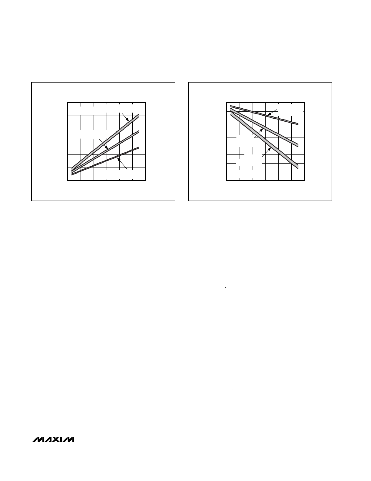
MAX1542/MAX1543
TFT LCD DC-to-DC Converter with
Operational Amplifiers
______________________________________________________________________________________ 17
negative charge-pump output voltages for a given
V
MAIN
for one-, two-, and three-stage charge pumps,
based on the following equations:
where G_ON is the positive charge-pump output voltage, G_OFF is the negative charge-pump output voltage, n is the number of charge-pump stages, and VDis
the voltage drop across each diode.
VDis the forward voltage drop of the charge-pump
diodes.
Flying Capacitors
Increasing the flying capacitor (C3, C4, and C5) value
increases the output current capability. Increasing the
capacitance indefinitely has a negligible effect on output current capability because the internal switch resistance and the diode impedance limit the source
impedance. A 0.1µF ceramic capacitor works well in
most low-current applications. The flying capacitor’s
voltage rating must exceed the following:
VCX> n ✕ V
MAIN
Where n is the stage number in which the flying capacitor appears, and V
MAIN
is the main output voltage. For
example, the two-stage positive charge pump in the
Typical Application Circuits (Figures 1 and 2) where
V
MAIN
= 8V contains two flying capacitors. The flying
capacitor in the first stage (C5) requires a voltage rat-
ing greater than 8V. The flying capacitor in the second
stage (C4) requires a voltage rating greater than 16V.
Charge-Pump Output Capacitor
Increasing the output capacitance or decreasing the
ESR reduces the output ripple voltage and the peak-topeak transient voltage. With ceramic capacitors, the
output voltage ripple is dominated by the capacitance
value. Use the following equation to approximate the
required capacitor value:
where V
RIPPLE
is the acceptable peak-to-peak output-
voltage ripple.
Charge-Pump Rectifier Diodes
To maximize the available output voltage, use Schottky
diodes with a current rating equal to or greater than two
times the average charge-pump input current. If the
loaded charge-pump output voltage is greater than
required, some or all of the Schottky diodes can be
replaced with low-cost silicon switching diodes with an
equivalent current rating. The charge-pump input current is:
where n is the number of charge-pump stages.
II n
CP IN CP OUT__
=×
C
I
FV
OUT
LOAD
OSC RIPPLE
≥
××2
GON V nV V
G OFF n V V
MAIN MAIN D
MAIN D
_()
_( )
=+ −
=− −
Figure 5. Positive Charge-Pump Output Voltage vs. V
MAIN
Figure 6. Negative Charge-Pump Output Voltage vs. V
MAIN
POSITIVE CHARGE-PUMP
OUTPUT VOLTAGE vs. V
60
= 0.3V TO 1V
V
D
50
40
2-STAGE CHARGE-PUMP
30
G_ON (V)
20
10
0
214
3-STAGE CHARGE-PUMP
1-STAGE CHARGE-PUMP
V
MAIN
MAIN
1210864
(V)
NEGATIVE CHARGE-PUMP
-0
-5
-10
-15
-20
-25
G_OFF (V)
-30
-35
-40
-45
OUTPUT VOLTAGE vs. V
2-STAGE
CHARGE-PUMP
3-STAGE
CHARGE-PUMP
VD = 0.3V TO 1V
214
V
MAIN
MAIN
1-STAGE
CHARGE-PUMP
1210864
(V)
Page 18

MAX1542/MAX1543
TFT LCD DC-to-DC Converter with
Operational Amplifiers
18 ______________________________________________________________________________________
Power Dissipation
The MAX1542/MAX1543s’ maximum power dissipation
depends on the thermal resistance from the IC die to
the ambient environment and the ambient temperature.
The thermal resistance depends on the IC package, PC
board copper area, other thermal mass, and airflow.
The MAX1542/MAX1543, with their exposed backside
pad soldered to 1in2of PC board copper, can dissipate
about 1.7W into +70°C still air. More PC board copper,
cooler ambient air, and more airflow increase the possible dissipation while less copper or warmer air
decreases the IC’s dissipation capability. The major
components of power dissipation are the power dissipated in the step-up converter and the power dissipated by the operational amplifiers.
Step-Up Converter
The largest portions of power dissipation in the step-up
converter are the internal MOSFET, inductor, and the
output diode. If the step-up converter has 90% efficiency, about 3% to 5% of the power is lost in the internal
MOSFET, about 3% to 4% in the inductor, and about
1% in the output diode. The rest of the 1% to 3% is distributed among the input and output capacitors and the
PC board traces. If the input power is about 3W, the
power lost in the internal MOSFET is about 90mW to
150mW.
Operational Amplifiers
The power dissipated in the operational amplifiers
depends on their output current, the output voltage,
and the supply voltage:
where I
OUT_(SOURCE)
is the output current sourced by
the operational amplifier, and I
OUT_(SINK)
is the output
current that the operational amplifier sinks.
In a typical case where the supply voltage is 8V and
the output voltage is 4V with an output source current
of 30mA, the power dissipated is 120mW.
Layout Procedure
Careful PC board layout and routing are required for
high-frequency switching power supplies to achieve
good regulation, high efficiency, and stability. Use the
following guidelines for good PC board layout:
1) Place the input capacitors close enough to the IC to
provide adequate bypassing (within 1.5cm).
Connect the input capacitors to IN with a wide trace.
Minimize the area of high-current loops by placing
the inductor, output diode, and output capacitors
near the input capacitors and near LX and PGND.
The high-current input loop goes from the positive
terminal of the input capacitor to the inductor, to the
IC’s LX pin, out PGND, and to the input capacitor
negative terminal. The high-current output loop is
from the positive terminal of the input capacitor to
the inductor, to the catch diode (D1), to the positive
terminal of the output capacitors, reconnecting
between the output capacitor and input capacitor
ground terminals. Connect these loop components
together with short, wide connections. Avoid using
vias in the high-current paths. If vias are unavoidable, use many vias in parallel to reduce resistance
and inductance.
2) Create a power ground island (PGND) consisting of
the input and output capacitor grounds, PGND pin,
and the SRC bypass capacitor and other chargepump components. Connect all of these together
with short, wide traces or a small ground plane.
Maximizing the width of the power ground traces
improves efficiency and reduces output voltage ripple and noise spikes.
Create an analog ground island (AGND) consisting
of the AGND pin, FB divider, the operation amplifier
dividers, the COMP and DEL capacitor ground connections, and the device’s exposed backside pad.
Connect the AGND and PGND islands by connecting the PGND pin directly to the exposed backside
pad. Make no other connections between these
separate ground planes.
3) Place the feedback voltage-divider resistors close to
FB. The divider’s center trace should be kept short.
Placing the resistors far away causes their FB traces
to become antennas that can pick up switching
noise. Avoid running the feedback trace near LX or
the switching nodes in the charge pumps.
4) Minimize the length and maximize the width of the
traces between the output capacitors and the load
for best transient response.
5) Minimize the size of the LX node while keeping it
wide and short. Keep the LX node away from the
feedback node (FB) and analog ground. Use DC
traces as shields if necessary.
Refer to the MAX1543 Evaluation Kit for an example of
proper board layout.
PD I V V
PD I V
SOURCE OUT SOURCE SUP OUT
SINK OUT SINK OUT
=×−
=×
_( ) _
_( ) _
()
Page 19
MAX1542/MAX1543
TFT LCD DC-to-DC Converter with
Operational Amplifiers
______________________________________________________________________________________ 19
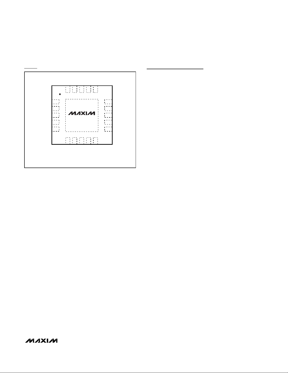
Pin Configurations (continued)
Chip Information
TRANSISTOR COUNT: 2508
PROCESS: BiCMOS
TOP VIEW
N.C.
CTL
DEL
COMP
FB
20
19
18
17
16
COM
SRC
N.C.
PGND
AGND
1
2
3
4
5
6
POS1
MAX1542
7
8
NEG1
OUT1
9
OUT2
THIN QFN
15
14
13
12
11
10
NEG2
N.C.
IN
LX
SUP
POS2
Page 20

MAX1542/MAX1543
TFT LCD DC-to-DC Converter with
Operational Amplifiers
Maxim cannot assume responsibility for use of any circuitry other than circuitry entirely embodied in a Maxim product. No circuit patent licenses are
implied. Maxim reserves the right to change the circuitry and specifications without notice at any time.
20 ____________________Maxim Integrated Products, 120 San Gabriel Drive, Sunnyvale, CA 94086 408-737-7600
© 2003 Maxim Integrated Products Printed USA is a registered trademark of Maxim Integrated Products.
Package Information
(The package drawing(s) in this data sheet may not reflect the most current specifications. For the latest package outline information,
go to www.maxim-ic.com/packages
.)
D
PIN # 1
I.D.
D/2
C
COMMON DIMENSIONS
A1
0.15 C A
E/2
A3
D2
0.15
C B
E
0.10
C
A
0.08 C
(NE-1) X e
DETAIL A
k
e
(ND-1) X e
L
L
e e
PROPRIETARY INFORMATION
TITLE:
PACKAGE OUTLINE
16, 20, 28, 32L, QFN THIN, 5x5x0.8 mm
APPROVAL
C
L
D2/2
b
0.10 M
PIN # 1 I.D.
0.35x45
E2/2
C
k
L
DOCUMENT CONTROL NO.
21-0140
C A B
QFN THIN.EPS
E2
L
CC
L
L
REV.
1
C
2
EXPOSED PAD VARIATIONS
NOTES:
1. DIMENSIONING & TOLERANCING CONFORM TO ASME Y14.5M-1994.
2. ALL DIMENSIONS ARE IN MILLIMETERS. ANGLES ARE IN DEGREES.
3. N IS THE TOTAL NUMBER OF TERMINALS.
4. THE TERMINAL #1 IDENTIFIER AND TERMINAL NUMBERING CONVENTION SHALL CONFORM TO JESD 95-1
SPP-012. DETAILS OF TERMINAL #1 IDENTIFIER ARE OPTIONAL, BUT MUST BE LOCATED WITHIN THE
ZONE INDICATED. THE TERMINAL #1 IDENTIFIER MAY BE EITHER A MOLD OR MARKED FEATURE.
5. DIMENSION b APPLIES TO METALLIZED TERMINAL AND IS MEASURED BETWEEN 0.25 mm AND 0.30 mm
FROM TERMINAL TIP.
6. ND AND NE REFER TO THE NUMBER OF TERMINALS ON EACH D AND E SIDE RESPECTIVELY.
7. DEPOPULATION IS POSSIBLE IN A SYMMETRICAL FASHION.
8. COPLANARITY APPLIES TO THE EXPOSED HEAT SINK SLUG AS WELL AS THE TERMINALS.
9. DRAWING CONFORMS TO JEDEC MO220.
10. WARPAGE SHALL NOT EXCEED 0.10 mm.
PROPRIETARY INFORMATION
TITLE:
PACKAGE OUTLINE
16, 20, 28, 32L, QFN THIN, 5x5x0.8 mm
21-0140
REV.DOCUMENT CONTROL NO.APPROVAL
2
C
2
 Loading...