

Page 1
General Description
The MAX1538 selector provides power-source control
for dual-battery systems. The device selects between
an AC adapter and dual batteries based on the presence of the three power sources and the state of
charge of each battery. The MAX1538 includes analog
comparators to detect AC/airline-adapter presence and
determine battery undervoltage. Fast analog circuitry
allows the device to switch between power sources to
implement a break-before-make time, which allows hot
swapping of battery packs. The MAX1538 independently performs power-source monitoring and selection, freeing the system power-management µP for
other tasks. This simplifies the development of µP
power-management firmware and allows the µP to enter
standby, reducing system power consumption.
The MAX1538 supports “relearn mode,” which allows
the system to measure and fully utilize battery capacity.
In this state, the part allows the selected battery to be
discharged even when an AC adapter is present. The
MAX1538 can also be used to power the system in an
aircraft. On detecting an airline adapter, the MAX1538
automatically disables charging or discharging of battery packs and only allows the system to be powered
from the adapter.
The MAX1538 is available in a space-saving 28-pin thin
QFN package with a maximum footprint of 5mm x 5mm.
Applications
Notebook and Subnotebook Computers
Internet Tablets
Dual-Battery Portable Equipment
Features
♦ Automatically Detects and Responds to
Low-Battery Voltage Condition
Battery Insertion and Removal
AC-Adapter Presence
Airline-Adapter Presence
♦ Step-Down and Step-Up Charger Compatibility
♦ Fast Break-Before-Make Selection
Allows Hot Swapping of Power Sources
No External Schottky Diodes Needed
♦ 50µA Maximum Battery Quiescent Current
♦ Implements Battery Capacity Relearning
♦ Allows Usage of Aircraft Supply
♦ Direct Drive of P-Channel MOSFETs
♦ Simplifies Power-Management µP Firmware
♦ 4.75V to 28V AC-Adapter Input Voltage Range
♦ Small 28-Pin Thin QFN Package (5mm x 5mm)
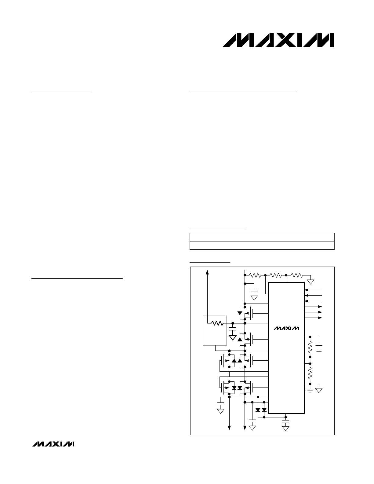
MAX1538
Power-Source Selector for
Dual-Battery Systems
________________________________________________________________ Maxim Integrated Products 1
19-3169; Rev 0; 1/04
For pricing, delivery, and ordering information, please contact Maxim/Dallas Direct! at
1-888-629-4642, or visit Maxim’s website at www.maxim-ic.com.
MAX1538
REVBLK
DISA
DISB
BATA
BATB
CHGB
CHGA
CHGIN
ADPIN
EXTLD
ADPBLK
AIRDET
ACDET
MINVA
MINVB
V
DD
CHRG
BATSEL
RELRN
OUT2
OUT1
OUT0
GND
BATSUP
BATTERY
CHARGER
CHG_OUT
SYSTEM LOAD
ADAPTER
BATTERY B
BATTERY A
Ordering Information
Pin Configuration appears at end of data sheet.
Typical Operating Circuit
PART TEMP RANGE PIN-PACKAGE
MAX1538ETI -40°C to +85°C 28 Thin QFN
Page 2

MAX1538
Power-Source Selector for
Dual-Battery Systems
2 _______________________________________________________________________________________
ABSOLUTE MAXIMUM RATINGS
ELECTRICAL CHARACTERISTICS
(V
BATA
= V
BATB
= V
CHGIN
= 16.8V, C
VDD
= 1µF, V
MINVA
= V
MINVB
= 0.93V, V
EXTLD
= V
ADPIN
= 28V, V
CHRG
= V
BATSEL
= V
RELRN
= 0,
C
ADPPWR
= C
REVBLK
= C
ADPBLK
= C
DISBAT
= C
DISA
= C
DISB
= C
CHGA
= C
CHGB
= 4.7nF, TA = 0°C to +85°C, unless otherwise noted.
Typical values are at T
A
= +25°C.)
Stresses beyond those listed under “Absolute Maximum Ratings” may cause permanent damage to the device. These are stress ratings only, and functional
operation of the device at these or any other conditions beyond those indicated in the operational sections of the specifications is not implied. Exposure to
absolute maximum rating conditions for extended periods may affect device reliability.
V
EXTLD
, V
BATSUP
, V
ADPIN
, V
BATA
, V
BATB
,
V
CHGIN
to GND .................................................-0.3V to +30V
V
ADPPWR
to GND...................................-0.3V to (V
ADPIN
+ 0.3V)
V
REVBLK
, V
ADPBLK
to GND ...................-0.3V to (V
EXTLD
+ 0.3V)
V
CHGA
, V
CHGB, VDISBAT
to GND ..........-0.3V to (V
CHGIN
+ 0.3V)
V
DISA
to GND..........................................-0.3V to (V
BATA
+ 0.3V)
V
DISB
to GND..........................................-0.3V to (V
BATB
+ 0.3V)
V
DD
, V
CHRG
, V
BATSEL
, V
RELRN
, V
OUT0
, V
OUT1
, V
OUT2
,
V
MINVA
, V
MINVB
, V
AIRDET
, V
ACDET
to GND..........-0.3V to +6V
Continuous Power Dissipation (T
A
= +70°C)
28-Pin Thin QFN 5mm x 5mm
(derate 20.8mW/°C above +70°C)..........................1666.7mW
Operating Temperature Range
MAX1538ETI ....................................................-40°C to +85°C
Junction Temperature......................................................+150°C
Storage Temperature Range .............................-65°C to +150°C
Lead Temperature (soldering, 10s) .................................+300°C
PARAMETER CONDITIONS
MIN
TYP
MAX
UNITS
ADPIN, EXTLD Supply Voltage
Range
V
CHGIN, BATA, BATB and
BATSUP Supply Voltage Range
V
V
ADPIN
= highest,
V
ADPPWR
= high
21 50
V
ADPIN
= highest,
V
ADPPWR
= low
23 54
V
BATA
= highest,
V
DISA
= high
21 42
24 50
V
BATB
= highest,
V
DISB
= high
21 42
24 50
ADPIN, BATA, BATB, BATSUP
Quiescent Current (Current from
the Highest Voltage Supply)
V
BATA
= 4.75V to 19V,
V
BATB
= 4.75V to 19V,
V
ADPIN
= 4.75V to 28V,
no external load at V
DD
V
BATSUP
= highest 18 40
µA
V
ADPPWR
= high
0.5
ADPIN Quiescent Current (ADPIN
Current When Not the Highest
Voltage)
V
ADPIN
= 4.75V to 18V,
no external load at V
DD
V
ADPPWR
= low 2.6 6
µA
V
DISA
= high 3.9 6.0
BATA Quiescent Current (BATA
Current When Not the Highest
Voltage)
V
BATA
= 4.75V to 19V,
no external load at V
DD
V
DISA
= low 7.0 12
µA
V
DISB
= high 3.9 6.0
BATB Quiescent Current (BATB
Current When Not the Highest
Voltage)
V
BATB
= 4.75V to 19V,
no external load at V
DD
V
DISB
= low 7.0 12
µA
Adapter selected (REVBLK or ADPBLK pins low) 3.0 6.1
EXTLD Quiescent Current
Adapter not selected (REVBLK and ADPBLK pins high)
1.0
µA
AC or ai r l i ne state ( C H G A, C H GB, and D IS BAT p i ns hi g h)
1.5
3.1 6.2
CHGIN Quiescent Current
Discharge or relearn state (CHGA or CHGB pin low,
DISBAT pin low)
6.1
µA
4.75 28.00
4.75 19.00
V
BATSUP
= 4.75V to 19V,
V
V
BATA
BATB
= highest, V
= highest, V
DISA
DISB
= low
= low
Charge state (CHGA or CHGB pin low, DISBAT pin high)
0.01
0.02
0.03
12.1
Page 3
MAX1538
Power-Source Selector for
Dual-Battery Systems
_______________________________________________________________________________________ 3
ELECTRICAL CHARACTERISTICS (continued)
(V
BATA
= V
BATB
= V
CHGIN
= 16.8V, C
VDD
= 1µF, V
MINVA
= V
MINVB
= 0.93V, V
EXTLD
= V
ADPIN
= 28V, V
CHRG
= V
BATSEL
= V
RELRN
= 0,
C
ADPPWR
= C
REVBLK
= C
ADPBLK
= C
DISBAT
= C
DISA
= C
DISB
= C
CHGA
= C
CHGB
= 4.7nF, TA = 0°C to +85°C, unless otherwise noted.
Typical values are at T
A
= +25°C.)
PARAMETER CONDITIONS
UNITS
LINEAR REGULATOR
VDD Output Voltage I
VDD
= 0 to 100µA
3.3
V
V
BATA
or V
BATB
= 5V to 19V, V
ADPIN
= 5V 1.0
V
BATA
= V
BATB
= 5V, V
ADPIN
= 5V to 28V 1.0
VDD Power-Supply Rejection
Ratio
V
BATA
, V
BATB
, or V
ADPIN
= 5V to 19V, sawtooth at
10V/µs, other supplies = 12V
1
mV / V
VDD Undervoltage Lockout Rising edge, relative to regulation point -55 -10 mV
COMPARATORS
ACDET, AIRDET Input Voltage
Range
0 5.5 V
ACDET, AIRDET Input Bias
Current
V
AIRDET
= V
ACDET
= 3V 0.1 1 µA
ACDET, AIRDET Trip Threshold Input falling
2.0
V
ACDET, AIRDET Hysteresis 20 mV
MINV_ Operating Voltage Range
V
MINV_ Input Bias Current V
MINV_
= 0.93V to 2.6V -50
nA
V
MINV_
= 0.93V
V
MINV_
= 1.5V
7.5
BAT_ Minimum Voltage Trip
Threshold
V
BAT_
falling
V
MINV_
= 2.6V
13
V
BAT_ Minimum Voltage
Hysteresis
mV
BAT_ Pack Removal Detection
Threshold
V
BAT_
falling
2.0
V
BAT_ Pack Removal Hysteresis 85 mV
GATE DRIVERS (Note 1)
V
SOURCE
= 15V, V
PIN
= 7.5V 18 60
ADPPWR, REVBLK, ADPBLK,
DISBAT, DISA, DISB, CHGA,
CHGB Source Current (PMOS
Turn-Off)
V
SOURCE
= 15V, V
PIN
= 13V 3 15
mA
V
SOURCE
= 15V, V
PIN
= 15V 20 70
ADPPWR, REVBLK, ADPBLK,
DISBAT, DISA, DISB, CHGA,
CHGB Sink Current (PMOS
Turn-On)
V
SOURCE
= 15V, V
PIN
= 9.5V 10 55
mA
V
SOURCE
= 8V to 28V)
ADPPWR, REVBLK, ADPBLK,
DISBAT, DISA, DISB, CHGA,
CHGB Turn-On Clamp Voltage
(V
PIN
to V
SOURCE
)
V
SOURCE
= 4.75V to 8V
V
MIN TYP MAX
3.270
1.97
0.93 2.60
4.605 4.65 4.695
7.455
12.93
1.90
V
= 8V to 19V (ADPPWR, REVBLK, and AOPBLK,
SOURCE
-11.0 -9.0 -7.0
-8.00 -3.65
125
3.330
2.03
+50
7.545
13.07
2.10
Page 4

MAX1538
Power-Source Selector for
Dual-Battery Systems
4 _______________________________________________________________________________________
ELECTRICAL CHARACTERISTICS (continued)
(V
BATA
= V
BATB
= V
CHGIN
= 16.8V, C
VDD
= 1µF, V
MINVA
= V
MINVB
= 0.93V, V
EXTLD
= V
ADPIN
= 28V, V
CHRG
= V
BATSEL
= V
RELRN
= 0,
C
ADPPWR
= C
REVBLK
= C
ADPBLK
= C
DISBAT
= C
DISA
= C
DISB
= C
CHGA
= C
CHGB
= 4.7nF, TA = 0°C to +85°C, unless otherwise noted.
Typical values are at T
A
= +25°C.)
PARAMETER
SYMBOL
CONDITIONS
MIN
TYP
MAX
UNITS
ADPPWR, REVBLK, ADPBLK,
DISBAT, DISA, DISB, CHGA,
CHGB Turn-On Time
0.3
µs
ADPPWR, REVBLK, ADPBLK,
DISBAT, DISA, DISB, CHGA,
CHGB Turn-Off Time
0.3
µs
STATE SELECTION INPUTS
CHRG, BATSEL, RELRN Input
Low Voltage
0.8 V
CHRG, BATSEL, RELRN Input
High Voltage
2.1 V
CHRG, BATSEL, RELRN Input
Leakage Current
V
CHRG
= V
BATSEL
= V
RELRN
= 5.5V 0.1 1 µA
STATE OUTPUTS
V
OUT_
= 0.4V 1
OUT0, OUT1, OUT2 Sink Current
V
OUT_
= 5.5V 25
mA
OUT0, OUT1, OUT2 Leakage
Current
0.1 1 µA
TRANSITION TIMES
MINV_ Comparator Delay t
MINV
V
BAT
_ = 5.5V to V
BAT
_ = 4.45V 5.5 11 µs
AIRDET and ACDET Comparator
Delay
t
ADP
Falling edge with -20mV overdrive 2.7 6.0 µs
BAT_ Removal Comparator Delay
Falling edge with -20mV overdrive 10 µs
Battery-Insertion Blanking Time t
BBLANK
13 21 31 ms
State-Machine Delay 50 ns
MOSFET Turn-On Delay t
TRANS
5 7.5 10 µs
V
OU T _
V
V
= 5.5V
SOURCE
SOURCE
= 15V, V
= 15V, V
= 13V to V
PIN
= 9V to V
PIN
PIN
PIN
= 9V
= 13V
0.88
0.88
Page 5
MAX1538
Power-Source Selector for
Dual-Battery Systems
_______________________________________________________________________________________ 5
ELECTRICAL CHARACTERISTICS
(V
BATA
= V
BATB
= V
CHGIN
= 16.8V, C
VDD
= 1µF, V
MINVA
= V
MINVB
= 0.93V, V
EXTLD
= V
ADPIN
= 28V, V
CHRG
= V
BATSEL
= V
RELRN
= 0,
C
ADPPWR
= C
REVBLK
= C
ADPBLK
= C
DISBAT
= C
DISA
= C
DISB
= C
CHGA
= C
CHGB
= 4.7nF, TA = -40°C to +85°C, unless otherwise noted.)
(Note 2)
PARAMETER CONDITIONS
UNITS
ADPIN, EXTLD Supply Voltage
Range
V
CHGIN, BATA, BATB, and
BATSUP Supply Voltage Range
V
V
ADPIN
= highest,
V
ADPPWR
= high
50
V
ADPIN
= highest,
V
ADPPWR
= low
54
42
50
42
50
ADPIN, BATA, BATB, BATSUP
Quiescent Current (Current from
the Highest Voltage Supply)
V
B AT A
= 4.75V to 19V ,
V
B AT B
= 4.75V to 19V ,
V
A D P IN
= 4.75V to 28V ,
no exter nal l oad at V
D D
V
BATSUP
= highest 40
µA
V
ADPPWR
= high 1
ADPIN Quiescent Current (ADPIN
Current When Not the Highest
Voltage)
V
ADPPWR
= low 9
µA
V
DISA
= high 7.5
BATA Quiescent Current (BATA
Current When Not the Highest
Voltage)
V
BATA
= 4.75V to 19V,
V
DISA
= low 16
µA
V
DISB
= high 7.5
BATB Quiescent Current (BATB
Current When Not the Highest
Voltage)
V
BATB
= 4.75V to 19V,
V
DISB
= low 16
µA
Adapter selected (REVBLK or ADPBLK pins low) 9.5
EXTLD Quiescent Current
Adapter not selected (REVBLK and ADPBLK pins high) 1.0
µA
AC or ai r l i ne state ( C H G A, C H GB, and D IS BAT p i ns hi g h) 1.5
10
CHGIN Quiescent Current
Discharge or relearn state (CHGA or CHGB pin low,
DISBAT pin low)
µA
LINEAR REGULATOR
VDD Output Voltage I
VDD
= 0 to 100µA
V
VDD Undervoltage Lockout Rising edge, relative to regulation point -60 -10 mV
COMPARATORS
ACDET, AIRDET Input Voltage
Range
0 5.5 V
ACDET, AIRDET Trip Threshold Input falling
V
MINV_ Operating Voltage Range
V
V
MINV_
= 0.93V
V
MINV_
= 1.5V 7.4 7.6
BAT_ Minimum Voltage Trip
Threshold
V
BAT_
falling
V
MINV_
= 2.6V
V
MIN MAX
4.75 28.00
4.75 19.00
V
B AT S U P
V
ADPIN
no external load at V
no external load at V
no external load at V
Charge state (CHGA or CHGB pin low, DISBAT pin high)
= 4.75V to 19V ,
= 4.75V to 18V,
= highest, V
BATA
V
= highest, V
BATA
V
= highest, V
BATB
V
BATB
= highest, V
DD
DD
DD
DISA
DISA
DISB
DISB
= high
= low
= high
= low
V
3.270 3.330
1.94 2.06
0.93 2.60
4.59 4.72
12.86 13.14
18.5
Page 6

MAX1538
Power-Source Selector for
Dual-Battery Systems
6 _______________________________________________________________________________________
PARAMETER
CONDITIONS
UNITS
BAT_ Pack Removal Detection
Threshold
V
BAT_
falling
V
GATE DRIVERS (Note 1)
V
SOURCE
= 15V, V
PIN
= 7.5V 18
ADPPWR, REVBLK, ADPBLK,
DISBAT, DISA, DISB, CHGA,
CHGB Source Current (PMOS
Turn-Off)
V
SOURCE
= 15V, V
PIN
= 13V 3
mA
V
SOURCE
= 15V, V
PIN
= 15V 20
ADPPWR, REVBLK, ADPBLK,
DISBAT, DISA, DISB, CHGA,
CHGB Sink Current (PMOS
Turn-On)
V
SOURCE
= 15V, V
PIN
= 9.5V 10
mA
V
S OU RC E
= 8V to 19V ( AD P P W R, RE V BLK,
and AD P BLK, V
S OU RC E
= 8V to 28V )
ADPPWR, REVBLK, ADPBLK,
DISBAT, DISA, DISB, CHGA,
CHGB Turn-On Clamp Voltage
(V
PIN
to V
SOURCE
)
V
SOURCE
= 4.75V to 8V
V
ADPPWR, REVBLK, ADPBLK,
DISBAT, DISA, DISB, CHGA,
CHGB Turn-On Time
µs
ADPPWR, REVBLK, ADPBLK,
DISBAT, DISA, DISB, CHGA,
CHGB Turn-Off Time
µs
STATE SELECTION INPUTS
CHRG, BATSEL, RELRN Input
Low Voltage
0.8 V
CHRG, BATSEL, RELRN Input
High Voltage
2.1 V
STATE OUTPUTS
1
25
mA
TRANSITION TIMES
MINV_ Comparator Delay t
MINV
V
BAT
_ = 5.5V to V
BAT
_ = 4.45V 11 µs
AIRDET and ACDET Comparator
Delay
t
ADP
Falling edge with -20mV overdrive 6 µs
Battery-Insertion Blanking Time t
BBLANK
12 31 ms
MOSFET Turn-On Delay t
TRANS
510µs
Note 1: V
PIN
refers to the voltage of the driver output. V
SOURCE
refers to the power source for the driver. ADPPWR, REVBLK, ADPBLK, DISBAT, DISA, DISB, CHGA, and CHGB gate drivers correspond to sources at ADPIN, EXTLD, EXTLD, CHGIN, BATA,
BATB, CHGIN, and CHGIN, respectively.
Note 2: Guaranteed by design. Not production tested.
ELECTRICAL CHARACTERISTICS (continued)
(V
BATA
= V
BATB
= V
CHGIN
= 16.8V, C
VDD
= 1µF, V
MINVA
= V
MINVB
= 0.93V, V
EXTLD
= V
ADPIN
= 28V, V
CHRG
= V
BATSEL
= V
RELRN
= 0,
C
ADPPWR
= C
REVBLK
= C
ADPBLK
= C
DISBAT
= C
DISA
= C
DISB
= C
CHGA
= C
CHGB
= 4.7nF, TA = -40°C to +85°C, unless otherwise noted.)
(Note 2)
SYMBOL
MIN MAX
1.88 2.12
OUT0, OUT1, OUT2 Sink Current
-11.7 -6.5
-8.00 -3.50
V
OU T _
V
OU T _
V
V
= 15V, V
SOURCE
= 15V, V
SOURCE
= 0.4V
= 5.5V
= 13V to V
PIN
= 9V to V
PIN
= 9V 0.88
PIN
= 13V 0.88
PIN
Page 7
MAX1538
Power-Source Selector for
Dual-Battery Systems
_______________________________________________________________________________________ 7
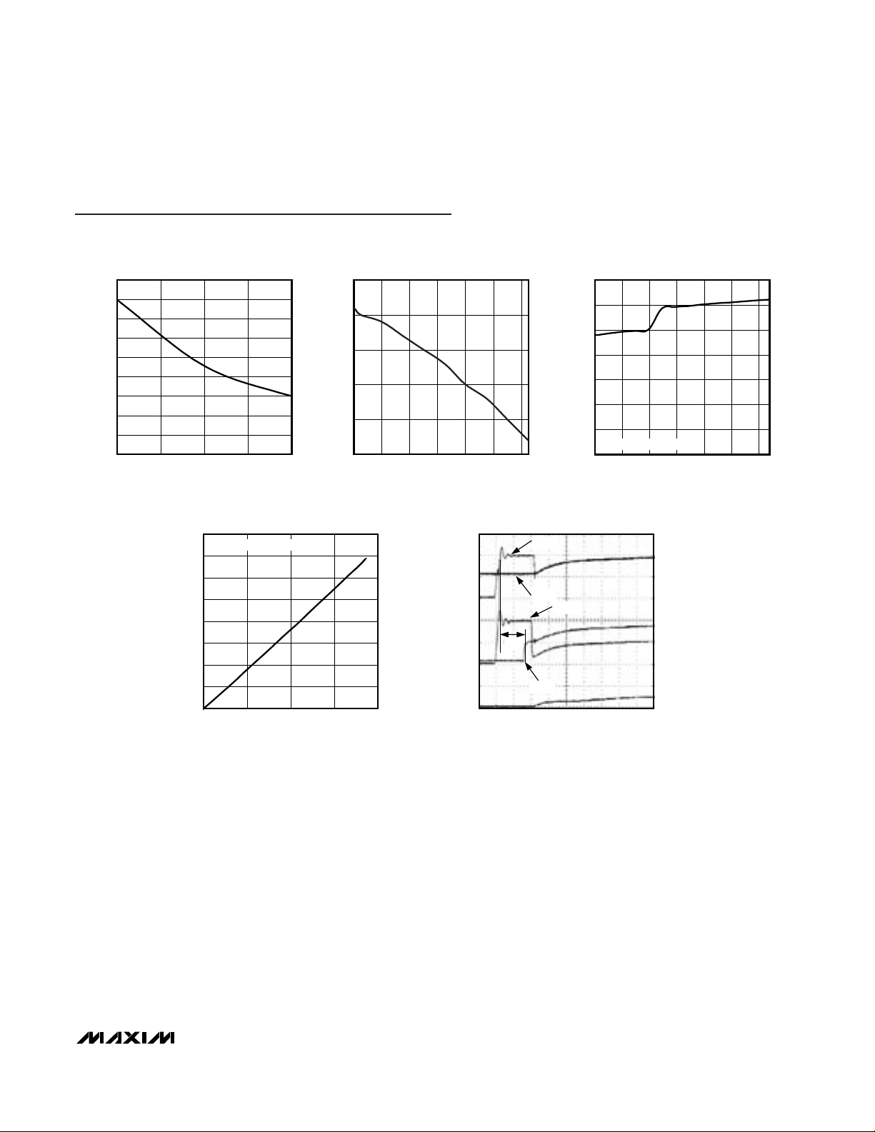
VDD LOAD REGULATION
MAX1538 toc01
VDD LOAD CURRENT (mA)
V
DD
(V)
0.150.100.05
3.291
3.292
3.293
3.294
3.295
3.296
3.297
3.298
3.299
3.290
00.20
VDD vs. TEMPERATURE
MAX1538 toc02
TEMPERATURE (°C)
V
DD
(V)
6040200-20
3.290
3.295
3.300
3.305
3.310
3.285
-40 80
I
BAT_
vs. V
BAT_
MAX1538 toc04
BATTERY VOLTAGE (V)
BATTERY INPUT CURRENT (µA)
15105
0.5
1.0
1.5
2.0
2.5
3.0
3.5
4.0
0
020
BAT_ NOT HIGHEST SUPPLY
I
BAT_
vs. V
BAT_
MAX1538 toc03
BATTERY VOLTAGE (V)
BATTERY INPUT CURRENT (µA)
14121086
5
10
15
20
25
30
35
0
416
BAT_ HIGHEST SUPPLY
Typical Operating Characteristics
(Circuit of Figure 1. TA = +25°C, unless otherwise noted.)
ADAPTER INSERTION
MAX1538 toc05
10.0µs/div
20V
10V
V
ADPIN
AND
V
EXTLD
V
ADPBLK
V
REVBLK
V
OUT1
0V
20V
10V
0V
5V
0V
V
ADPIN
V
EXTLD
V
REVBLK
V
ADPBLK
t
ADP
Page 8

MAX1538
Power-Source Selector for
Dual-Battery Systems
8 _______________________________________________________________________________________
Typical Operating Characteristics (continued)
(Circuit of Figure 1. TA = +25°C, unless otherwise noted.)
SOURCE SELECTION CHANGE
MAX1538 toc10
2.00µs/div
0V
10V
0V
5V
V
DISB
(10V/div)
V
DISA
(10V/div)
V
BATB
AC-COUPLED
(5V/div)
V
BATSEL
V
OUT0
10V
20V
10V
t
TRANS
INDUCTIVE KICK
NO CAPACITOR
AT BATB
BATTERY INSERTION
MAX1538 toc06
5.00ms/div
10V
0V
V
DISB
(10V/div)
V
OUT0
(10V/div)
V
DISA
V
BATA
V
EXTLD
0V
10V
10V
0V
20V
10V
SYSTEM LOAD = 3A
V
BATB
= 16.8V
V
BATA
= 10V
A
B
A:
CONTACT BOUNCE
B: BATTERY INSERTION BLANKING TIME = 22ms
BATTERY REMOVAL TIMING
MAX1538 toc08
4.00µs/div
10V
10.2V
9.8V
V
OUT0
(10V/div)
V
DISB
V
DISA
V
EXTLD
9.6V
10V
0V
10V
0V
0V
5 x MINV
t
MINV
(t
ADP
FOR
ADAPTER
REMOVAL
TIMING)
t
TRANS
V
BATA
= 16.8V
BATTERY B
REMOVED
SYSTEM LOAD = 3A
SOURCE SELECTION CHANGE
MAX1538 toc09
2.00µs/div
0V
10V
0V
5V
V
DISB
(10V/div)
V
DISA
(10V/div)
V
BATB
AC-COUPLED
(5V/div)
V
BATSEL
V
OUT0
10V
20V
10V
t
TRANS
INDUCTIVE KICK
C
BATB
= 1µF
SYSTEM LOAD = 3A
BATTERY REMOVAL
MAX1538 toc07
5.00ms/div
10V
0V
V
DISB
(10V/div)
V
OUT0
(10V/div)
V
DISA
V
BATA
V
EXTLD
0V
10V
10V
0V
20V
10V
CONTACT BOUNCE
V
BATB
= 16.8V
V
BATA
= 10V
Page 9

MAX1538
Power-Source Selector for
Dual-Battery Systems
_______________________________________________________________________________________ 9
PIN NAME FUNCTION
1
Minimum Battery A Voltage Set Point. Battery A discharge is prevented if V
BATA
has fallen below 5 x
V
MINVA
.
2
Minimum Battery B Voltage Set Point. Battery B discharge is prevented if V
BATB
has fallen below 5 x
V
MINVB
.
3
Battery-Selection Input. Drive to logic low to charge battery A or give discharge preference to battery A.
Drive to logic high to charge battery B or give discharge preference to battery B.
4
Battery-Relearn Logic-Level Input. Drive RELRN high to enable battery-relearn mode.
5 CHRG
Charge-Enable Logic-Level Input. Drive CHRG high to enable the charging path from the charger to the
battery selected by BATSEL.
6 OUT0
7 OUT1
8 OUT2
Selector-State Output. This open-drain output indicates the state of the MAX1538. See Table 1 for
information on decoding.
9
AC-Adapter Detection Input. When V
ACDET
is greater than the ACDET trip threshold (2V typ), adapter
presence is detected.
10
Airline-Adapter Detection Input. When V
AIRDET
> 2V and V
ACDET
< 2V, the airline-adapter presence is
detected. Charging is disabled when an airline adapter is detected.
11
Adapter Input. When V
ADPIN
> V
BATSUP
, the MAX1538 is powered by ADPIN. ADPIN is the supply rail for
the ADPPWR MOSFET driver.
12
Adapter-Power P-Channel MOSFET Driver. Connect ADPPWR to the gate of P1 (Figure 1). P1 disconnects
the adapter from the system during relearn mode. Exclude P1 and leave ADPPWR disconnected if relearn
is not used. ADPPWR is driven relative to ADPIN. ADPPWR and REVBLK are driven with the same control
signal.
13
Gate Drive for the Reverse-Blocking P-Channel MOSFET. Connect REVBLK to the gate of P2 (Figure 1). P2
enables and disables the AC adapter’s power path. REVBLK is driven relative to EXTLD. REVBLK and
ADPPWR are driven with the same control signal.
Typical Operating Characteristics (continued)
(Circuit of Figure 1. TA = +25°C, unless otherwise noted.)
Pin Description
MINVA
MINVB
BREAK-BEFORE-MAKE TIMING
t
TRANS
MOSFET
TURN-OFF
TIME
MOSFET
TURN-ON
MOSFET FOR INITIAL
DISCHARGE PATH
TIME
MOSFET FOR FINAL
DISCHARGE PATH
1.00µs/div
MAX1538 toc11
16V
14V
12V
10V
8V
MOSFET
DRIVERS
FIRST SOURCE INSERTION
POWER-UP TIME
200µs/div
MAX1538 toc12
5V
OUT1
0V
OUT2, OUT0
V
20V
ADPIN
V
10V
REVBLK
0V
20V
V
EXTLD
10V
0V
BATSEL
RELRN
ACDET
AIRDET
ADPIN
ADPPWR
REVBLK
Page 10

MAX1538
Power-Source Selector for
Dual-Battery Systems
10 ______________________________________________________________________________________
PIN NAME FUNCTION
14
Gate Drive for the Adapter-Blocking P-Channel MOSFET. Connect ADPBLK to the gate of P3 (Figure 1). P3
enables and disables the battery discharge path. ADPBLK is driven relative to EXTLD. ADPBLK and
DISBAT are driven with the same control signal.
15, 21 N.C. Not Internally Connected
16
External Load. EXTLD is the supply rail for REVBLK and ADPBLK.
17
Charger Node Input. CHGIN is the supply rail for DISBAT, CHGA, and CHGB.
18
Gate Drive for the Battery-Discharge P-Channel MOSFET. Connect DISBAT to the gate of P4 (Figure 2). P4
disconnects the battery from the system load when charging from a step-up converter. Exclude P4 and
leave DISBAT disconnected if using a step-down charger. DISBAT is driven relative to CHGIN. DISBAT and
ADPBLK are driven by the same control signal.
19 CHGA
Gate Drive for the Charge Battery A P-Channel MOSFET. Connect CHGA to the gate of P6 (Figure 1). P6
enables and disables the charge path into battery A. CHGA is driven relative to CHGIN. CHGA and DISA
are driven by the same control signal.
20 CHGB
Gate Drive for the Charge Battery B P-Channel MOSFET. Connect CHGB to the gate of P7 (Figure 1). P7
enables and disables the charge path into battery B. CHGB is driven relative to CHGIN. CHGB and DISB
are driven by the same control signal.
22 BATB
Battery B Voltage Input. Battery undervoltage and absence is determined by measuring BATB. BATB is the
supply rail for DISB.
23 DISB
Gate Drive for the Discharge from Battery B P-Channel MOSFET. Connect DISB to the gate of P8 (Figure 1).
P8 enables and disables the discharge path from battery B. DISB is driven relative to BATB. DISB and
CHGB are driven by the same control signal.
24 DISA
Gate Drive for the Discharge from Battery A P-Channel MOSFET. Connect DISA to the gate of P5 (Figure 1).
P5 enables and disables the discharge path from battery A. DISA is driven relative to BATA. DISA and
CHGA are driven by the same control signal.
25 BATA
Battery A Voltage Input. Battery undervoltage and absence is determined by measuring BATA. BATA is the
supply rail for DISA.
26
BATSUP powers the MAX1538. Diode OR BATA and BATB to BATSUP externally. ADPIN is diode
connected to BATSUP internally. Bypass with a 0.1µF capacitor from BATSUP to GND.
27 GND Ground
28 V
DD
Linear-Regulator Output. Bypass with a 1µF capacitor from VDD to GND.
Pin Description (continued)
ADPBLK
EXTLD
CHGIN
DISBAT
BATSUP
Page 11

MAX1538
Power-Source Selector for
Dual-Battery Systems
______________________________________________________________________________________ 11
MAX1538
REVBLK
DISA
DISB
BATA
BATB
CHGB
CHGA
CHGIN
ADPIN
EXTLD
ADPBLK
BATTERY A
BATTERY B
AIRDET
ACDET
MINVA
MINVB
V
DD
CHRG
BATSEL
RELRN
OUT2
OUT1
OUT0
GNDBATSUP
ADAPTER
ADPPWR
R1 R2 R3
P1
IN
P2
P3
P5
P6P7
P8
STEP-DOWN CHARGER
C
SYS
C
CHG
C2
FOR RELEARN
MODE ONLY
C
BATB
C
BATA
D1
D2
R10
R11
R12
R13
C1
0.1µF
LOGIC SUPPLY
R
SNS
SYSTEM LOAD
CHARGER OUTPUT
C
ADAPTER
C3
0.1µF
CHARGER INPUT
OUT
Figure 1. Step-Down Typical Application Circuit
Page 12

MAX1538
Power-Source Selector for
Dual-Battery Systems
12 ______________________________________________________________________________________
MAX1538
REVBLK
DISA
DISB
BATB
CHGB
CHGA
CHGIN
ADPIN
DISBAT
BATTERY A
BATTERY B
AIRDET
ACDET
OUT
MINVA
MINVB
GND
V
DD
CHRG
BATSEL
RELRN
OUT2
OUT1
OUT0
BATA BATSUP
ADAPTER
ADPPWR
R1 R2 + R3
P1
IN
P2
P4
P5
P6P7
P8
STEP-UP CHARGER
C
SYS
C2
FOR RELEARN
MODE ONLY
C
BATB
C
BATA
D1
D2
R10
R11
R12
R13
C1
1µF
LOGIC SUPPLY
CHARGER OUTPUT
C
ADAPTER
C3
0.1µF
CHARGER INPUT
C
CHG
EXTLD
ADPBLK
P3
EXTERNAL AC/AIR-
DETECTION CIRCUIT
OUT
SYSTEM LOAD
Figure 2. Typical Application Circuit for Step-Up/Step-Down Charger
Page 13

MAX1538
Power-Source Selector for
Dual-Battery Systems
______________________________________________________________________________________ 13
ACDET
AIRDET
V
DD
GND
ADPIN
LDO
REF
BATSUP
2V
MINVA
BATA
R
4R
0.4V
MINVB
BATB
R
4R
0.4V
BATSEL
RELRN
CHRG
ADPIN
ADPPWR
EXTLD
REVBLK
CHGIN
DISBAT
ADPBLK
CHGA
CHGB
BATA
DISA
BATB
DISB
OUT1
OUT2
OUT0
STATE
MACHINE
R
S
Q
BATTERY B
UNDERVOLTAGE
LATCH
MAX1538
NNN
Q
R
S
Q
BATTERY A
UNDERVOLTAGE
LATCH
Q
Figure 3. Functional Diagram
Page 14

Power-Source Selector for
Dual-Battery Systems
14 ______________________________________________________________________________________
Detailed Description
The MAX1538 performs power path selection between
an adapter input and two batteries, relieving the host
system from the burden of real-time response to powersource changes. The integrated selector implements a
fixed break-before-make timer to ensure that power
sources are not connected together and yet the load is
not left unserviced. The MAX1538 monitors battery and
adapter state and presence to determine which source
to select and whether to charge the battery. Logic
inputs CHRG, BATSEL, and RELRN allow the host to
enable/disable charging, select which battery to use,
and impose battery discharge even with adapter presence. The MAX1538 automatically detects airline
adapters and prevents charging when an airline
adapter is detected. Open-drain logic outputs OUT2,
OUT1, and OUT0 indicate the state of the selector so
the host can properly respond.
The MAX1538 can be configured for use with a stepdown battery charger, as shown in Figure 1, or with a
step-up/step-down battery charger, as shown in Figure
2. The minimum MAX1538 system requires only six
MOSFETs. The MAX1538 provides relearn-mode support with the addition of P1. Relearn mode allows the
system to relearn the battery’s capacity without user
intervention.
Table 1 summarizes the possible states and configura-
tions of the MAX1538.
SOURCE STATE
MOSFET STATE (See Figure 4)
Battery
Adapter
B
CHG
RELRN
BATSEL
System
(ADPPWR
Battery
(ADPBLK
BATT A
DISA)
BATT B
DISB)
OUT2
OUT1
OUT0
STATE
AC
X
0 On Off On Off
Charge A
AC
X
1 On Off Off On
Charge B
AC
X
0 Off On On Off
Relearn A
AC
1 Off On Off On
Relearn B
AC Otherwise On Off Off Off
AC adapter
AIR
X
On Off Off Off
Airline
Absent
X
0
Absent
Off On On Off
Absent
1
Absent
Off On Off On
Absent
Off Off Off Off
Idle
Legend
AC AC adapter is present. V
ACDET
and V
AIRDET
are both above 2V.
AIR Airline adapter is present. V
ACDET
is below 2V and V
AIRDET
is above 2V.
Absent
External adapter is absent. V
ACDET
and V
AIRDET
are both below 2V.
N indicates the battery is normal. The battery is normal when it has not tripped the undervoltage latch (5 x
V
MINV_
). See the Battery Presence and Undervoltage Detection section.
U indicates the battery has tripped the undervoltage comparator. An undervoltage battery is detected
when V
BAT_
goes below 5 x V
MINV_
. See the Battery Presence and Undervoltage Detection section.
Otherwise Otherwise covers all cases not explicitly shown elsewhere in the table.
X
X indicates don’t care. The output does not depend on any inputs labeled X.
Table 1. MAX1538 State Table
MAX1538
LOGIC INPUTS
A
X
X
N
X N X 1
X
N
NUXX X
X N XX
UNXX X
UUXX X
10
10
X 1
XX X
XX
and REVBLK)
and DISBAT)
(CHGA and
(CHGB and
110
111
100
101
010
011
000Discharge A
001Discharge B
000
N
U
X
XX X
Page 15

MAX1538
Power-Source Selector for
Dual-Battery Systems
______________________________________________________________________________________ 15
Battery Presence and
Undervoltage Detection
The MAX1538 determines battery absence and undervoltage and does not allow discharge from an undervoltage battery. A battery is considered undervoltage
when V
BAT_
< 5 x V
MINV_
, and remains classified as
undervoltage until V
BAT_
falls below 2V and again rises
above 5 x V
MINV
. The undervoltage latch is also
cleared when the charge path is enabled. Set the battery undervoltage threshold using resistive voltagedividers R10, R11, R12, and R13, as shown in Figure 1.
The corresponding undervoltage threshold is:
To minimize error, use 1% or better accuracy divider
resistors, and ensure that the impedance of the divider
results in a current about 100 times the MINV_ input
bias current at the MINV_ threshold voltage. To optimize error due to 50nA input bias current at MINV_ and
minimize current consumption, typically choose resistors (R10 + R11) or (R12 + R13) smaller than 600kΩ.
Since batteries often exhibit large changes in their terminal voltage when a load current is removed, further
discharge after the undervoltage latch has been set is
not allowed until the battery is removed or the charge
path to the battery is selected. Battery removal is
detected when V
BAT_
falls below 2V. For correct detection of battery removal, ensure that the leakage current
into BAT_ is lower than the leakage current out of BAT_
so that BAT_ falls below 2V when the battery is
removed. The contributors to leakage current into BAT_
are D1, D2, P6, and P7.
Battery Relearn Mode
The MAX1538 implements a battery relearn mode,
which allows for host-device manufacturers to implement a mode for coulomb-counting fuel gauges (such
as the MAX1781) to measure battery capacity without
user intervention. In battery relearn mode, the AC
adapter is switched off and battery discharge is selected. In this implementation, the host system could
prompt users when their battery capacity becomes
inaccurate, use the host system as a load to discharge
the battery, and then recharge the battery fully.
Coulomb-counting fuel-gauge accuracy is increased
after a relearning cycle.
Battery relearn mode requires the addition of MOSFET
P1, which blocks current from the adapter to the system. To enable relearn mode, drive RELRN high and
drive BATSEL low to relearn battery A or high to relearn
battery B. Relearn mode overrides the functionality of
the CHG pin. Battery relearn mode does not occur
when the selected battery’s undervoltage latch has
been set, or when the selector is in airline mode (see
the Airline Mode and AC Adapter section.) The RELRN
pin only applies when an AC adapter is present. If the
AC adapter is absent and RELRN is ignored, OUT[2:1]
= 10 when the MAX1538 is in battery relearn mode. If
CHG = 0, only OUT2 is needed to indicate that the
MAX1538 was properly placed in relearn mode.
If the selected battery trips the undervoltage latch when
in relearn mode, the AC adapter is switched in without
causing a crash to the system. OUT2 can indicate that
the relearn cycle is terminated due to battery undervoltage. Typically, after the host system performs a battery
relearn cycle, it either charges the discharged battery
or begins a relearn cycle on the other battery. To switch
to charge mode, drive RELRN low and CHG high.
Since RELRN overrides CHG, in many applications it is
best to permanently keep CHG high and reduce the IO
needed to control the selector.
When the AC adapter is available, it is used as the
power source for EXTLD unless the RELRN pin is high.
In this state, the charger can be enabled and a
battery charged.
VV
R
RR
VV
R
RR
BATA Undervoltage DD
BATB Undervoltage DD
_
_
=× ×
+
=× ×
+
5
11
10 11
5
13
12 13
ADAPTER
ADAPTER
SWITCH
SYSTEM
BATTERY
SWITCH
CHARGER
"A"
SWITCH
"B"
SWITCH
BATTERY A
BATTERY B
ADAPTER
ADAPTER
SWITCH
SYSTEM
BATTERY
SWITCH
CHARGER
"A"
SWITCH
"B"
SWITCH
BATTERY A
BATTERY B
ADAPTER
ADAPTER
SWITCH
SYSTEM
BATTERY
SWITCH
CHARGER
"A"
SWITCH
"B"
SWITCH
BATTERY A
BATTERY B
CHARGE DISCHARGE/
RELEARN
AC/AIR
Figure 4. MAX1538 Selection States
Page 16

MAX1538
Power-Source Selector for
Dual-Battery Systems
16 ______________________________________________________________________________________
Airline Mode and AC Adapter
The MAX1538 provides compatibility with airline
adapters. For airplane safety, the use of an airline
adapter requires that the battery charger or charge
path is disabled. The MAX1538 disables the charge
path when an airline adapter is detected. In airline
mode, ADPPWR and REVBLK drive P1 and P2 on, and
all other MOSFETs are off, regardless of the state of
RELRN, CHG, BATSEL, or the batteries. If the AC
threshold is above the airline threshold, select a resistive voltage-divider (as shown in Figure 1) according to
the following equations:
where V
ACDET_Threshold
and V
AIRDET_Threshold
are typically 2.0V (see the Electrical Characteristics). An AC
adapter is detected when the adapter voltage is above
V
AC_Threshold
, and an airline adapter is detected when
the adapter voltage is between V
AC_Threshold
and
V
AIR_Threshold
.
To minimize error, use 1% accuracy or better divider
resistors, and ensure that the impedance of the divider
results in a current about 100 times the ACDET and
AIRDET input bias current. To optimize error due to 1µA
input bias current at ACDET/AIRDET and minimize current consumption, typically choose R3 less than 20kΩ.
See the Adapter Removal Debouncing section for more
information regarding R1, R2, and R3. Short R2 to disable airline-adapter mode.
Optionally, an external circuit can be implemented to
determine the presence of an AC/airline adapter. The
circuit in Figure 5 provides fast detection of an airline
adapter, yet allows external circuitry to discriminate
between airline and AC adapters. If V
AC_Threshold
<
V
AIR_Threshold
, this circuit must be used for airlineadapter detection. Other permutations that directly
drive AIRDET instead do not work properly on the
MAX1538 because adapter removal is not detected
fast enough, causing the system load to crash.
OUT[2:0] = 011 if the MAX1538 is in airline-adapter
mode. If RELRN = 0 and CHG = 0, only OUT[1:0] are
necessary to indicate airline-adapter mode.
VV
RR R
R
VV
RR R
RR
AC Threshold ACDET Threshold
Air Threshold AIRDET Threshold
__
__
=×
++
=×
++
+
12 3
3
12 3
23
MAX1538
EXTERNAL AC/AIRLINE
DETECTION CIRCUIT
REVBLK
ADPIN
EXTLD
AIRDET
ACDET
ADAPTER
ADPPWR
R1 R2 + R3
P1
P2
OUT
ACDET
ADPIN
ADAPTER INSERTION
ACDET
ADPIN
ADAPTER REMOVAL
ACDET MUST WAIT
ACDET MAY OCCUR
BEFORE OR AFTER ADPIN
FOR AC ADAPTER
FOR AIRLINE ADAPTER
FOR AC ADAPTER
FOR AIRLINE ADAPTER
Figure 5. Using an External Adapter Detection Circuit
Page 17

MAX1538
Power-Source Selector for
Dual-Battery Systems
______________________________________________________________________________________ 17
CHG Control
Toggle CHG to enable the charge path to the battery.
Charge control is overridden by RELRN (see the Battery
Relearn Mode section) or airline mode (see the Airline
Mode and AC Adapter section). When CHG is enabled,
the MAX1538 connects the selected battery (BATSEL = 0
for battery A and BATSEL = 1 for battery B) to the charger. OUT[2:1] = 11 if the MAX1538 is in charge mode.
When the charge path is enabled, the corresponding
battery undervoltage latch is cleared. This allows charging of protected battery packs. In typical applications,
connect CHRG to VDD to reduce the system I/O.
Single Transition Break-Before-Make
Selection
The MAX1538 guarantees that no supplies are connected to each other during any transition by implementing
a fixed delay time (t
TRANS
, the break-before-make transition timer). This is necessary as the batteries have very
low impedances, and momentarily shorting batteries
together can cause hundreds of amps to flow. For
example, when adapter removal is detected, ADPPWR
and REVBLK begin to turn off less than 10µs before
ADPBLK and DISBAT begin to turn on, connecting the
appropriate battery. For example, upon switching from
one battery to another, DISA and CHGA begin turning
off less than 10µs before DISB and CHGB begin to turn
on. To guarantee a break-before-make time, ensure that
the turn-off time of the MOSFETs is smaller than t
TRANS
(see the MOSFET Selection section).
The MAX1538 also guarantees that any change does
not cause unnecessary power-source transitions. When
switching from battery to battery; battery to adapter; or
adapter to battery because of adapter or battery insertion or removal, or due to a change at BATSEL, a single
set of MOSFETs are turned off followed by another set
of MOSFETs turned on. No additional transitions are
necessary. The only exception occurs when RELRN is
high and the adapter is inserted because it is first
detected as an airline adapter and later detected as an
AC adapter. This results in a transition from discharge
mode to AC mode, followed by a transition from AC
mode to relearn mode. Although this extra transition is
generally harmless, it can be avoided by disabling
relearn mode when the adapter is absent.
Blanking
The MAX1538 implements sophisticated blanking at the
adapter and the batteries to correctly determine battery/adapter insertion and removal. Logic inputs CHRG,
RELRN, and BATSEL should be debounced to ensure
that fast repetitive transitions do not occur, in which
case the system holdup capacitor is not large enough
to sustain the system load.
Battery insertion is automatically debounced using the
battery-insertion blanking time (t
BBLANK
). A battery is
not discharged unless the battery has been above the
5 x V
MINV
threshold for 21ms (typ). After t
BBLANK
is
expired, V
BAT_
must exceed 5 x V
MINV_
or the battery
is detected as undervoltage.
Applications Information
MOSFET Selection
Select P-channel MOSFETs P1–P8 according to their
power dissipation, R
DSON
, and gate charge. Each
MOSFET must be rated for the full system load current.
Additionally, the battery discharge MOSFETs (P3, P5,
P6, P7, and P8) should be selected with low on-resistance for high discharge efficiency. Since for any given
switch configuration at least half of the MOSFETs are
off, dual MOSFETs can be used without reducing the
effective MOSFET power dissipation. When using dual
MAX1538
DISA
BATA
DISB
CHGB
CHGA
CHGIN
ADPIN
ADPBLK
BATTERY A
BATTERY B
ADPPWR
P1
P2
P5
P6P7
P8
REVBLK
EXTLD
P3
SYSTEM LOAD
FOR RELEARN
MODE ONLY
DUAL
FDS4935A
DUAL
FDS4935A
DUAL
FDS4935A
STEP-DOWN
BATTERY CHARGER
IN
OUT
BATB
ADAPTER
Figure 6. Optimal Use of Power Dissipation Using Dual
MOSFETs
Page 18

MAX1538
Power-Source Selector for
Dual-Battery Systems
18 ______________________________________________________________________________________
MOSFETs, they should be paired as shown in Figure 6
for optimal power dissipation.
The MAX1538 provides asymmetric MOSFET gate
drive, typically turning MOSFETs on faster than they are
turned off. The t
TRANS
timer ensures that the MOSFETs
that are turning on begin to turn on 10µs after those
MOSFETs that are turning off begin to turn off. Choose
MOSFETs with low enough gate charge that all off-transitioning MOSFETs turn off before any on-transitioning
MOSFET turns on. Use the following equations to estimate the worst-case turn-on and turn-off times:
where t
ON
is the turn-on time, t
OFF
is the turn-off time,
Q
G
is the MOSFET’s total gate charge specified at volt-
age VG, I
OFF1
is the 18mA (min) gate current when dri-
ving the gate from 7.5V gate drive to 2V gate drive, ∆V
1
is the voltage change during the 18mA gate drive
(5.5V), I
OFF2
is 3mA gate current when driving the gate
from 2V to 0V, ∆V
2
is the 2V change, and IONis the
turn-on current.
The MAX1538’s gate-drive current is nonlinear and is a
function of gate voltage. For example, the gate driver
slows down as the MOSFET approaches off. See the
Typical Operating Characteristics for a scope shot
showing MAX1538 turn-on and turn-off times when driving FDS6679 MOSFETs. The MAX1538 typically turns
the FDS6679 on in 0.7µs and off in 1µs.
Combining the MAX1538 with a Charger
To configure the MAX1538 for use with a step-down
charger, use the circuit of Figure 7. Connect the charger’s power input to EXTLD. Do not connect the charger’s power input to ADPIN. This ensures that the
charger does not bias ADPIN through its high-side
MOSFET.
System Holdup Capacitor
C
SYS
must be capable of sustaining the maximum system load during the transition time between source
selection. Size the capacitor so that:
where t
MINV
is the battery undervoltage comparator
delay, t
TRANS
is the fixed time between switching
MOSFETs off and switching MOSFETs on, tONis the
time to turn a MOSFET on (see the MOSFET Selection
section), V
MINV
is the lower of V
MINVA
and V
MINVB
,
I
SYS_MAX
is the maximum system load, V
SYS_MIN
is the
minimum allowable system voltage before system
5× − ++
()
×
>
Vtt t
I
C
V
MINV MINV TRANS ON
SYS MAX
SYS
SYS MIN
_
_
t
Q
VVI
V
I
Q
V
k
t
Q
VVI
Q
V
k
ON
G
GOFF OFF
G
G
ON
G
GONGG
=
∆
+
∆
=× Ω
=×=× Ω
1
1
2
2
093
5
025..
MAX1538
MAX1908
MAX1909 OR
MAX1535
REVBLK
CHGIN
ADPIN
DCIN
P2
C
SYS
C2
EXTLD
ADPBLK
P3
SYSTEM LOAD
CSSP
CSSN
1µF
BATT
ADAPTER
C
ADAPTER
Figure 7. Combining the MAX1538 with a Charger
Page 19

MAX1538
Power-Source Selector for
Dual-Battery Systems
______________________________________________________________________________________ 19
crash, and C
SYS
is the total system holdup capacitance, which does not need to be near the MAX1538.
The timing related to the system holdup capacitance is
shown in Figure 8.
Charger output capacitance contributes to C
SYS
for the
step-down charger topology (Figure 1), but not for the
step-up/step-down charger topology (Figure 2).
Leakage Current into BAT_
Leakage current into BATA or BATB can interfere with
proper battery-removal detection. D1 and D2 must be
low leakage to ensure that battery removal is properly
detected. Choose MOSFETs P6 and P7 with low offleakage current. Board leakage current can also be a
problem. For example, neighbor pins BATA and
BATSUP should have greater than 50MΩ impedance
between each other. Proper battery-removal detection
requires that:
where I
Board
is board leakage current, I
DS_OFF
is the
off-leakage current of MOSFETs P6 and P7, I
D_Leakage
is the reverse leakage current of the diodes, and
I
BAT_Sink@2V
is the BAT_ leakage current at 2V (0.4µA;
see the Typical Operating Characteristics).
Inductive “Kick”
When the adapter or a battery is delivering a significant
current to the system and that path is disabled (typically to enable another path), a voltage spike is generated
at the source. This is due to a parasitic inductance
shown in Figure 9. When the adapter is disconnected, a
positive voltage spike occurs at ADPIN. When a discharging battery is disconnected, a positive voltage
spike occurs at BAT_. Connect a capacitor from BAT_
or ADPIN to GND to limit this inductive kick. Choose the
source capacitance according to the following equation:
where V
SOURCE
is the maximum DC voltage of the
source in question, I
SYS_MAX
is the maximum system
load, and L
SOURCE
(parasitic inductance) and
C
SOURCE
are shown in Figure 9.
During battery charge, the voltage spike during battery
disconnect is negative. To ensure that this negative
voltage spike does not go below 0V, choose C
BAT_
according to the following equation:
C
LI
V
BAT
BAT CHG MAX
BAT MIN
_
__
__
>
×
2
2
C
LI
V
SOURCE
SOURCE SYS MAX
SOURCE
_
>
×
−
2
2
2
30
II I I
II
Board DS OFF P DS OFF P D leakage
D leakage BAT Sink V
++++
<
_() _() _
__@
671
22
ADPBLK/REVBLK
REVBLK/ADPBLK
t
OFF
t
TRANS
t
ON
V
SYS_MIN
OTHER POWER SOURCE
EXTLD
5 x V
MINV
OR AC/AIR THRESHOLD
t
MINV
OR t
ADP
Figure 8. System Holdup Capacitor Timing
TO BATTERY
OR ADAPTER
PARASITIC
INDUCTANCE
(L
SOURCE
)
I
SOURCE
C
SOURCE
MAX1538
Figure 9. Inductive Kick Upon Source Disconnect
Page 20

MAX1538
Power-Source Selector for
Dual-Battery Systems
20 ______________________________________________________________________________________
where V
BAT__MIN
is the minimum battery voltage,
I
CHG_MAX
is the maximum charge current, and L
BAT_
is
the battery’s inductance. C
BAT_
values of 0.01µF are
adequate for typical applications. Adding capacitance
at BAT_ pins lengthens the time needed to detect battery removal. See the Battery-Absence-Detection Delay
section.
Adapter Removal Debouncing
Upon adapter removal the adapter’s connector may
bounce. To avoid false detection of adapter reinsertion
select R1, R2, and R3 according to the following equation:
where V
Adapter
is the AC-adapter voltage when removing an AC adapter and airline-adapter voltage when
removing an airline adapter, C
ADPIN
is the capacitance
at ADPIN, and t
Bounce
is the 5ms debounce time. See
the Airline Mode and AC Adapter section for a defini-
tion of V
_Threshold
.
Battery-Absence-Detection Delay
When a selected battery is removed, the system load
quickly pulls BAT_ below 5 x V
MINV_
and another
source is selected. The battery is considered present
and undervoltage until V
BAT_
falls below 2V. Although
another power source is quickly switched to the system
load, capacitance at BAT_ (see the Inductive "Kick"
section) delays the detection of the removed battery. If
another battery is inserted before this delay has
passed, it is considered undervoltage. Calculate the
delay using the following equation:
where I
BAT_
is the 3.9µA BAT_ quiescent current (due to
a 5MΩ internal resistor), and C
BAT_
is the capacitance
from BAT_ to GND. When C
BAT_
= 1µF, t
Absence_delay
corresponds to a 5s time constant. If this time is unacceptable, use a smaller capacitance or connect a resistor or current sink from BAT_ to GND.
Layout
The MAX1538 selector fits in a very small layout.
Ensure that C1 is placed close to VDDand GND.
Connect the paddle to GND directly under the IC. A
complete layout example is shown in Figure 10.
Because BATA and BATB are high-impedance nodes,
prevent leakage current between BATA/BATB and
other high-voltage sources by carefully routing traces.
Note that flux remaining on the board can significantly
contribute to leakage current. See the Leakage Current
into BAT_ section.
Minimize parasitic inductance in the BATA and BATB
path to reduce inductive kick during battery disconnect. This reduces the capacitance requirement at
BATA and BATB.
Chip Information
TRANSISTOR COUNT: 5431
PROCESS: BiCMOS
t
VC
I
Absence delay
BAT__
=×19
RR R
Vt
CV V
Threshold Bounce
ADPIN Adapter Threshold
12 3
_
_
++<
×
× −
()
28
27
26
25
24
23
22
21
20
19
18
17
16
15
8
9
10
11
12
13
14
1
2
3
4
5
6
7
VDDGND
BATSUP
BATA
DISA
DISB
BATB
MINVA
MINVB
BATSEL
RELRN
CHRG
OUT0
OUT1
OUT2
ACDET
AIRDET
ADPIN
ADPPWR
REVBLK
ADPBLK
N.C.
CHGB
CHGA
DISBAT
CHGIN
EXTLD
N.C.
MAX1538 *
THIN QFN
(5mm x 5mm)
*EXPOSED PADDLE
Pin Configuration
Page 21

MAX1538
Power-Source Selector for
Dual-Battery Systems
______________________________________________________________________________________ 21
BATSUP
2
4
MAX1538
28
27
25
24
23
22
21
18
15
9
10
11
12
13
14
GND
DISA
DISB
BATB
MINVA
ACDET
AIRDET
ADPIN
ADPPWR
REVBLK
ADPBLK
N.C.
CHGA
DISBAT
CHGIN
EXTLD
N.C.
20
19
17
16
R1
R10
R3
R11
R2
GND
GND
C
BATSUP
1
2
3
8
7
6
5
1
3
7
6
5
P8
P5
P6
P7
2134
8765
P3 P2
GND
C
ADAPTER
BATTERY B
BATTERY A
CHARGER
ADAPTER
SYSTEM
* EXPOSED PADDLE
CHGB
8
123
BATSEL
4
RELRN
8
567
CHRG
OUT0
OUT1
OUT2
MINVB
V
DD
C1
GND
C
BATB
GND
C
BATA
4
BATA
26
Figure 10. MAX1538 Layout Example
Page 22

MAX1538
Power-Source Selector for
Dual-Battery Systems
Maxim cannot assume responsibility for use of any circuitry other than circuitry entirely embodied in a Maxim product. No circuit patent licenses are
implied. Maxim reserves the right to change the circuitry and specifications without notice at any time.
22 ____________________Maxim Integrated Products, 120 San Gabriel Drive, Sunnyvale, CA 94086 408-737-7600
© 2004 Maxim Integrated Products Printed USA is a registered trademark of Maxim Integrated Products.
Package Information
(The package drawing(s) in this data sheet may not reflect the most current specifications. For the latest package outline information,
go to www.maxim-ic.com/packages
.)
QFN THIN.EPS
D2
(ND-1) X e
e
D
C
PIN # 1
I.D.
(NE-1) X e
E/2
E
0.08 C
0.10
C
A
A1
A3
DETAIL A
0.15
C B
0.15 C A
DOCUMENT CONTROL NO.
21-0140
PACKAGE OUTLINE
16, 20, 28, 32L, QFN THIN, 5x5x0.8 mm
PROPRIETARY INFORMATION
APPROVAL
TITLE:
C
REV.
2
1
E2/2
E2
0.10 M
C A B
PIN # 1 I.D.
b
0.35x45∞
L
D/2
D2/2
L
C
L
C
e e
L
CC
L
k
k
L
L
2
2
21-0140
REV.DOCUMENT CONTROL NO.APPROVAL
PROPRIETARY INFORMATION
TITLE:
COMMON DIMENSIONS
EXPOSED PAD VARIATIONS
1. DIMENSIONING & TOLERANCING CONFORM TO ASME Y14.5M-1994.
2. ALL DIMENSIONS ARE IN MILLIMETERS. ANGLES ARE IN DEGREES.
3. N IS THE TOTAL NUMBER OF TERMINALS.
4. THE TERMINAL #1 IDENTIFIER AND TERMINAL NUMBERING CONVENTION SHALL CONFORM TO JESD 95-1
SPP-012. DETAILS OF TERMINAL #1 IDENTIFIER ARE OPTIONAL, BUT MUST BE LOCATED WITHIN THE
ZONE INDICATED. THE TERMINAL #1 IDENTIFIER MAY BE EITHER A MOLD OR MARKED FEATURE.
5. DIMENSION b APPLIES TO METALLIZED TERMINAL AND IS MEASURED BETWEEN 0.25 mm AND 0.30 mm
FROM TERMINAL TIP.
6. ND AND NE REFER TO THE NUMBER OF TERMINALS ON EACH D AND E SIDE RESPECTIVELY.
7. DEPOPULATION IS POSSIBLE IN A SYMMETRICAL FASHION.
8. COPLANARITY APPLIES TO THE EXPOSED HEAT SINK SLUG AS WELL AS THE TERMINALS.
9. DRAWING CONFORMS TO JEDEC MO220.
NOTES:
10. WARPAGE SHALL NOT EXCEED 0.10 mm.
C
PACKAGE OUTLINE
16, 20, 28, 32L, QFN THIN, 5x5x0.8 mm
 Loading...