

Page 1
General Description
The MAX1530/MAX1531 multiple-output power-supply
controllers generate all the supply rails for thin-film transistor (TFT) liquid-crystal display (LCD) monitors. Both
devices include a high-efficiency, fixed-frequency,
step-down regulator. The low-cost, all N-channel, synchronous topology enables operation with efficiency as
high as 93%. High-frequency operation allows the use
of small inductors and capacitors, resulting in a compact solution. The MAX1530 includes three linear regulator controllers and the MAX1531 includes five linear
regulator controllers for supplying logic and LCD bias
voltages. A programmable startup sequence enables
easy control of the regulators.
The MAX1530/MAX1531 include soft-start functions to
limit inrush current during startup. An internal stepdown converter current-limit function and a versatile
overcurrent shutdown protect the power supplies against
fault conditions. The MAX1530/MAX1531 use a currentmode control architecture, providing fast load transient
response and easy compensation. An internal linear
regulator provides MOSFET gate drive and can be
used to power small external loads.
The MAX1530/MAX1531 can operate from inputs as
high as 28V and are well suited for LCD monitor and TV
applications running directly from AC/DC wall adapters.
Both devices are available in a small (5mm x 5mm),
ultra-thin (0.8mm), 32-pin QFN package and operate
over the -40°C to +85°C temperature range.
Applications
LCD Monitors and TVs
Automotive LCDs
Features
♦ 4.5V to 28V Input Voltage Range
♦ 250kHz/500kHz Current-Mode Step-Down Converter
Small Inductor/Capacitors
No Sense Resistor
♦ Three Positive Linear Regulator Controllers
One Positive and One Negative Additional
Controller (MAX1531)
Small Input and Output Capacitors
♦ Timed Reset Output
♦ Uncommitted Overcurrent Protection (MAX1531)
♦ Soft-Start for All Regulators
♦ Programmable Input Undervoltage Comparator
♦ Programmable Startup Sequencing
MAX1530/MAX1531
Multiple-Output Power-Supply Controllers for
LCD Monitors
________________________________________________________________ Maxim Integrated Products 1
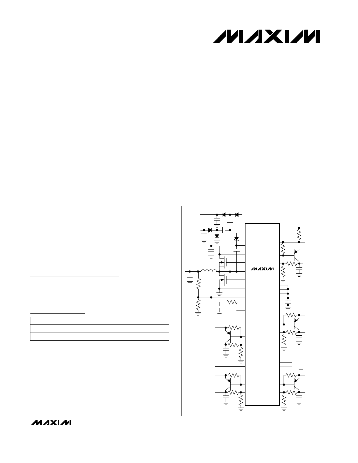
Ordering Information
RESET
V
IN
V
GON
25V
V
GOFF
-9V
V
IN
= 12V
ONL2
V
SOURCE
10V/500mA
V
GAMMA
9.7V
V
N
ONL5
ONL4
ONL3
SEQ
VL
RSTIN
V
OUT
3.3V/1.5A
V
LOGIC
2.5V/500mA
V
OUT
V
L
V
L
V
P
V
N
V
IN
V
IN
V
P
V
L
DRV3
FBL3
FBL1
DRV1
BST
IN
DH
LX
DL
PGND
FB
COMP
FBL2
DRV2
FBL5
DRV5
DRV4
FBL4
CSH
CSL
FREQ
ILIM
VL
EN
AGND
MAX1530
Minimal Operating Circuit
19-2866; Rev 0; 5/03
For pricing, delivery, and ordering information, please contact Maxim/Dallas Direct! at
1-888-629-4642, or visit Maxim’s website at www.maxim-ic.com.
Pin Configuration appears at end of data sheet.
PART TEMP RANGE PIN-PACKAGE
MAX1530ETJ -40°C to +85°C 32 Thin QFN
MAX1531ETJ -40°C to +85°C 32 Thin QFN
Page 2
MAX1530/MAX1531
Multiple-Output Power-Supply Controllers for
LCD Monitors
2 _______________________________________________________________________________________
ABSOLUTE MAXIMUM RATINGS
ELECTRICAL CHARACTERISTICS
(Circuit of Figure 1, VIN= 12V, VEN= V
SEQ
= 5V, TA = 0°C to +85°C, unless otherwise noted. Typical values are at TA= +25°C.)
Stresses beyond those listed under “Absolute Maximum Ratings” may cause permanent damage to the device. These are stress ratings only, and functional
operation of the device at these or any other conditions beyond those indicated in the operational sections of the specifications is not implied. Exposure to
absolute maximum rating conditions for extended periods may affect device reliability.
IN, DRV1, DRV2, DRV3, DRV4, CSH,
CSL to AGND .....................................................-0.3V to +30V
DRV5 to VL .............................................................-28V to +0.3V
CSH to CSL ..............................................................-0.3V to +6V
VL to AGND ..............................................................-0.3V to +6V
PGND to AGND...................................................................±0.3V
LX to BST..................................................................-6V to +0.3V
BST to AGND..........................................................-0.3V to +36V
DH to LX .....................................................-0.3V to (BST + 0.3V)
DL to PGND ..................................................-0.3V to (VL + 0.3V)
SEQ, ONL2, ONL3, ONL4, ONL5, COMP,
ILIM to AGND............................................-0.3V to (VL + 0.3V)
RSTIN, RESET, EN, FB, FBL1, FBL2, FBL3, FBL4, FBL5,
FREQ to AGND.....................................................-0.3V to +6V
VL Short Circuit to AGND ...........................................Momentary
Continuous Power Dissipation (T
A
= +70°C)
32-Pin Thin QFN (derate 21.3mW/°C above +70°C) ...1702mW
Operating Temperature Range ...........................-40°C to +85°C
Storage Temperature Range .............................-65°C to +150°C
Junction Temperature......................................................+150°C
Lead Temperature (soldering, 10s) .................................+300°C
GENERAL
PARAMETER CONDITIONS MIN TYP MAX UNITS
Operating Input Voltage Range (Note 1) 4.5 28.0 V
Quiescent Supply Current V
FB
= V
FBL1
= V
FBL2
= V
IC Disable Supply Current EN = AGND 200 400 µA
VL REGULATOR
VL Output Voltage 5.5V < V
VL Undervoltage Lockout
Threshold
VL rising, 3% hysteresis 3.2 3.5 3.8 V
< 28V, 0 < IVL < 30mA 4.75 5 5.25 V
IN
CONTROL AND SEQUENCE
SEQ, FREQ Input Logic High
Level
SEQ, FREQ Input Logic Low
Level
SEQ, FREQ Input Leakage
Current
2.0 V
0.6 V
-1 +1 µA
ONL_ Input Threshold ONL_ rising, 25mV hysteresis 1.201 1.238 1.275 V
ONL_ Source Current SEQ = EN = VL, V
_ = 0 to 1.24V 1.8 2.0 2.2 µA
ONL
ONL_ Input Leakage Current SEQ = EN = VL, ONL_ = VL -500 +500 nA
ONL_ Input Discharge Clamp
Resistance
SEQ = 0 800 1500 3000 Ω
EN Input Threshold EN rising, 5% hysteresis 1.201 1.238 1.275 V
EN Input Leakage Current -50 +50 nA
FAULT DETECTION
FB, FBL1, FBL2, FBL3, FBL4
Undervoltage Fault Trip Level
FBL5 Undervoltage Fault
Trip Level
FB, FBL1, FBL2, FBL3, FBL4 falling, 25mV hysteresis 1.081 1.114 1.147 V
FBL5 rising, 25mV hysteresis 300 400 500 mV
FBL3
= V
FBL4
= 1.5V, V
= 0 1.7 3.0 mA
FBL5
Page 3
MAX1530/MAX1531
Multiple-Output Power-Supply Controllers for
LCD Monitors
_______________________________________________________________________________________ 3
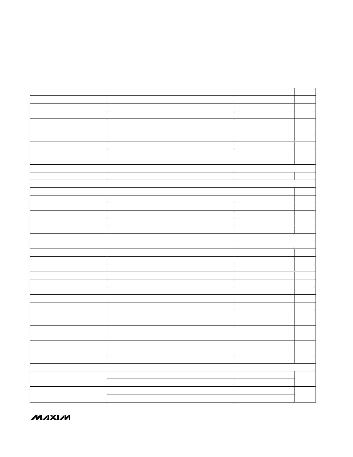
ELECTRICAL CHARACTERISTICS (continued)
(Circuit of Figure 1, VIN= 12V, VEN= V
SEQ
= 5V, TA = 0°C to +85°C, unless otherwise noted. Typical values are at TA= +25°C.)
Dual Mode is a trademark of Maxim Integrated Products, Inc.
PARAMETER CONDITIONS MIN TYP MAX UNITS
Comparator Bandwidth For EN, FB, FBL_ 10 kHz
Duration to Trigger Fault Latch For FB, FBL_ 51 64 77 ms
Overcurrent Protection Threshold (V
Overcurrent Sense Common-
Mode Range
CSH Input Current V
CSL Input Current V
Overcurrent Sense Filter RC Time
Constant
- V
) 270 300 330 mV
CSL
, V
CSL
= 2.7V to 28V 100 µA
= V
= 12V -50 +50 nA
CSH
2.7 28.0 V
V
CSH
CSH
CSH
CSL
50 µs
THERMAL PROTECTION
Thermal Shutdown Temperature rising, 15°C hysteresis 160 °C
RESET FUNCTION
RSTIN Reset Trip Level RSTIN falling, 25mV hysteresis 1.081 1.114 1.147 V
RSTIN Input Leakage Current V
= 1.5V -50 +50 nA
RSTIN
Comparator Bandwidth 10 kHz
Reset Timeout Period 102 128 154 ms
RESET Output Low Level I
RESET Output High Leakage V
= -1mA 0.4 V
RESET
= 5V 1 µA
RESET
STEP-DOWN CONTROLLER
ERROR AMPLIFIER
FB Regulation Voltage 1.223 1.238 1.253 V
Transconductance FB to COMP 70 100 140 µS
Voltage Gain FB to COMP 200 V/V
Minimum Duty Cycle 15 %
FB Input Leakage Current V
= 1.5V -50 +50 nA
FB
FB Input Common-Mode Range (Note 2) -0.1 +1.5 V
COMP Output Minimum Voltage V
COMP Output Maximum Voltage V
Current-Sense Amplifier Voltage
Gain
Current-Limit Threshold
(Default Mode)
Current-Limit Threshold
(Adjustable Mode)
= 1.5V 1 V
FB
= 1.175V 3 V
FB
V
IN
- V
LX
2.75 3.5 4.0 V/V
PGND - LX, ILIM = VL 190 250 310 mV
PGND - LX, V
= 1.25V 190 250 310 mV
ILIM
ILIM Inp ut D ual M od e™ Thr eshol d 3.0 3.5 4.00 V
OSCILLATOR
Switching Frequency
Maximum Duty Cycle
FREQ = AGND 200 250 300
FREQ = VL 425 500 575
FREQ = AGND 75 80 88
FREQ = VL 75 80 88
kHz
%
Page 4
MAX1530/MAX1531
Multiple-Output Power-Supply Controllers for
LCD Monitors
4 _______________________________________________________________________________________
ELECTRICAL CHARACTERISTICS (continued)
(Circuit of Figure 1, VIN= 12V, VEN= V
SEQ
= 5V, TA = 0°C to +85°C, unless otherwise noted. Typical values are at TA= +25°C.)
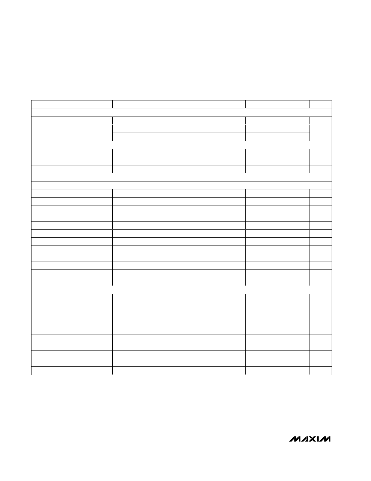
PARAMETER CONDITIONS MIN TYP MAX UNITS
SOFT-START
Step Size Measured at FB 1.238 / 32 V
Period
FET DRIVERS
DH, DL On-Resistance 3 10 Ω
DH, DL Output Drive Current Sourcing or sinking, V
LX, BST Leakage Current V
POSITIVE LINEAR REGULATOR (LR1)
FBL1 Regulation Voltage V
FBL1 Input Bias Current V
FBL1 Effective Load Regulation
Error (Transconductance)
FBL1 Line Regulation Error I
DRV1 Sink Current V
DRV1 Off-Leakage Current V
FBL1 Input Common-Mode
Range
Soft-Start Step Size Measured at FBL1 1.238 / 32 V
Soft-Start Period
POSITIVE LINEAR REGULATORS (LR2 AND LR3)
FBL_ Regulation Voltage V
FBL_ Input Bias Current V
FBL_ Effective Load Regulation
Error (Transconductance)
FBL_ Line Regulation Error I
DRV_ Sink Current V
DRV_ Off-Leakage Current V
FBL_ Input Common-Mode
Range
Soft-Start Step Size Measured at FBL_ 1.238 / 32 V
FREQ = GND 1024 / f
FREQ = VL 2048 / f
BST
= V
LX
or VDL = V
DH
= V
= 28V 20 µA
IN
/ 2 0.5 A
VL
OSC
OSC
LINEAR REGULATOR CONTROLLERS
= 5V, I
DRV1
= 1.5V -50 +50 nA
FBL1
V
= 5V, I
DRV1
= 100µA, 5.5V < VIN < 28V 5 mV
DRV1
= 1.175V, V
FBL1
= 1.5V, V
FBL1
= 100µA 1.226 1.245 1.264 V
DRV1
= 100µA to 2mA -1.5 -2 %
DRV1
= 5V 3 10 mA
DRV1
= 28V 0.1 10 µA
DRV1
(Note 2) -0.1 +1.5 V
FREQ = GND 1024 / f
FREQ = VL 2048 / f
_ = 5V, I
DRV
_ = 1.5V -50 +50 nA
FBL
V
_ = 5V, I
DRV
_ = 100µA, 5.5V < VIN < 28V 5 mV
DRV
= 1.175V, V
FBL_
_ = 1.5V, V
FBL
_ = 100µA 1.226 1.245 1.264 V
DRV
_ = 50µA to 1mA -1.5 -2 %
DRV
= 5V 2 4 mA
DRV_
_ = 28V 0.1 10 µA
DRV
OSC
OSC
(Note 2) -0.1 +1.5 V
s
s
Page 5
MAX1530/MAX1531
Multiple-Output Power-Supply Controllers for
LCD Monitors
_______________________________________________________________________________________ 5
ELECTRICAL CHARACTERISTICS (continued)
(Circuit of Figure 1, VIN= 12V, VEN= V
SEQ
= 5V, TA = 0°C to +85°C, unless otherwise noted. Typical values are at TA= +25°C.)
ELECTRICAL CHARACTERISTICS
(Circuit of Figure 1, VIN= 12V, VEN= V
SEQ
= 5V, TA = -40°C to +85°C, unless otherwise noted.) (Note 3)
PARAMETER CONDITIONS MIN TYP MAX UNITS
Soft-Start Period
POSITIVE LINEAR REGULATOR (LR4)
FBL4 Regulation Voltage V
FBL4 Input Bias Current V
FBL4 Effective Load Regulation
Error (Transconductance)
FBL4 Line Regulation Error I
DRV4 Sink Current V
DRV4_Off-Leakage Current V
FBL4 Input Common-Mode
Range
Soft-Start Step Size Measured at FBL4 1.238 / 32 V
Soft-Start Period
NEGATIVE LINEAR REGULATOR (LR5)
FBL5 Regulation Voltage V
FBL5 Input Bias Current V
FBL5 Effective Load Regulation
Error (Transconductance)
FBL5 Line Regulation Error I
DRV5 Source Current V
DRV5 Off-Leakage Current V
FBL5 Input Common-Mode
Range
Soft-Start Step Size Measured at FBL5 1.238 / 32 V
Soft-Start Period
FREQ = GND 1024 / f
FREQ = VL 2048 / f
= 5V, I
DRV4
= 1.5V -50 +50 nA
FBL4
V
= 5V, I
DRV4
= 500µA, 5.5V < VIN < 28V 5 mV
DRV4
= 1.175V, V
FBL4
= 1.5V, V
FBL4
= 500µA 1.226 1.245 1.264 V
DRV4
= 500µA to 10mA -1.5 -2 %
DRV4
= 5V 10 28 mA
DRV4
= 28V 0.1 10 µA
DRV4
OSC
OSC
(Note 2) -0.1 +1.5 V
FREQ = GND 1024 / f
FREQ = VL 2048 / f
= -10V, I
DRV5
= 0 -50 +50 nA
FBL5
V
= -10V, I
DRV5
= 100µA, 5.5V < VIN < 28V 5 mV
DRV5
= 200mV, V
FBL5
= 0, V
FBL5
DRV5
= 100µA 100 125 150 mV
DRV5
= 50µA to 1mA -1.5 -2 %
DRV5
= -10V 2 9 mA
DRV5
= -20V 0.1 10 µA
OSC
OSC
(Note 2) -0.1 +1.5 V
FREQ = AGND 1024 / f
FREQ = VL 2048 / f
OSC
OSC
s
s
s
PARAMETER CONDITIONS MIN TYP MAX UNITS
GENERAL
Operating Input Voltage Range (Note 1) 4.5 28.0 V
VL REGULATOR
VL Output Voltage 5.5V < V
VL Undervoltage Lockout
Threshold
VL rising, 3% hysteresis 3.2 3.8 V
< 28V, 0 < IVL < 30mA 4.75 5.25 V
IN
Page 6
MAX1530/MAX1531
Multiple-Output Power-Supply Controllers for
LCD Monitors
6 _______________________________________________________________________________________
ELECTRICAL CHARACTERISTICS (continued)
(Circuit of Figure 1, VIN= 12V, VEN= V
SEQ
= 5V, TA = -40°C to +85°C, unless otherwise noted.) (Note 3)
Note 1: Operating supply range is guaranteed by VL line regulation test for the range of 5.5V to 28V. Between 4.5V and 5.5V, the V
L
regulator might be in dropout; however, the part continues to operate properly.
Note 2: Guaranteed by design and not production tested.
Note 3: Specifications to -40°C are guaranteed by design and not production tested.
PARAMETER CONDITIONS MIN TYP MAX UNITS
CONTROL AND SEQUENCE
ONL_ Input Threshold ONL_ rising, 25mV hysteresis 1.201 1.275 V
EN Input Threshold EN rising, 5% hysteresis 1.201 1.275 V
FAULT DETECTION
FB, FBL1, FBL2, FBL3, FBL4
Fault Trip Level
FBL5 Fault Trip Level FBL5 rising, 25mV hysteresis 300 500 mV
Overcurrent Protection Threshold (V
RESET FUNCTION
RSTIN Reset Trip Level RSTIN falling, 25mV hysteresis 1.081 1.147 V
ERROR AMPLIFIER
FB Regulation Voltage 1.215 1.260 V
Current-Limit Threshold
(Default Mode)
Current-Limit Threshold
(Adjustable Mode)
POSITIVE LINEAR REGULATOR (LR1)
FBL1 Regulation Voltage V
FBL1 Input Bias Current V
POSITIVE LINEAR REGULATORS (LR2 AND LR3)
FBL_ Regulation Voltage V
FBL_ Input Bias Current V
POSITIVE LINEAR REGULATOR (LR4)
FBL4 Regulation Voltage V
FBL4 Input Bias Current V
NEGATIVE LINEAR REGULATOR (LR5)
FBL5 Regulation Voltage V
FBL5 Input Bias Current V
DRV5 Source Current V
FB, FBL1, FBL2, FBL3, FBL4 falling, 25mV hysteresis 1.081 1.147 V
- V
CSH
) 270 330 mV
CSL
STEP-DOWN CONTROLLER
PGND - LX, ILIM = VL 170 330 mV
PGND - LX, V
= 1.25V 170 330 mV
ILIM
LINEAR REGULATOR CONTROLLERS
= 5V, I
DRV1
= 1.5V
FBL1
_ = 5V, I
DRV
_ = 1.5V -50 +50 nA
FBL
= 5V, I
DRV4
= 1.5V -50 +50 nA
FBL4
= -10V, I
DRV5
= 0 -50 +50 nA
FBL5
= 200mV, V
FBL5
= 100µA 1.220 1.270 V
DRV1
-50 +50 nA
_ = 100µA 1.220 1.270 V
DRV
= 500µA 1.220 1.270 V
DRV4
= 100µA 100 150 mV
DRV5
= -10V 2 mA
DRV5
Page 7
MAX1530/MAX1531
Multiple-Output Power-Supply Controllers for
LCD Monitors
_______________________________________________________________________________________ 7
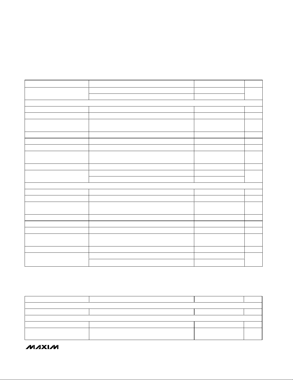
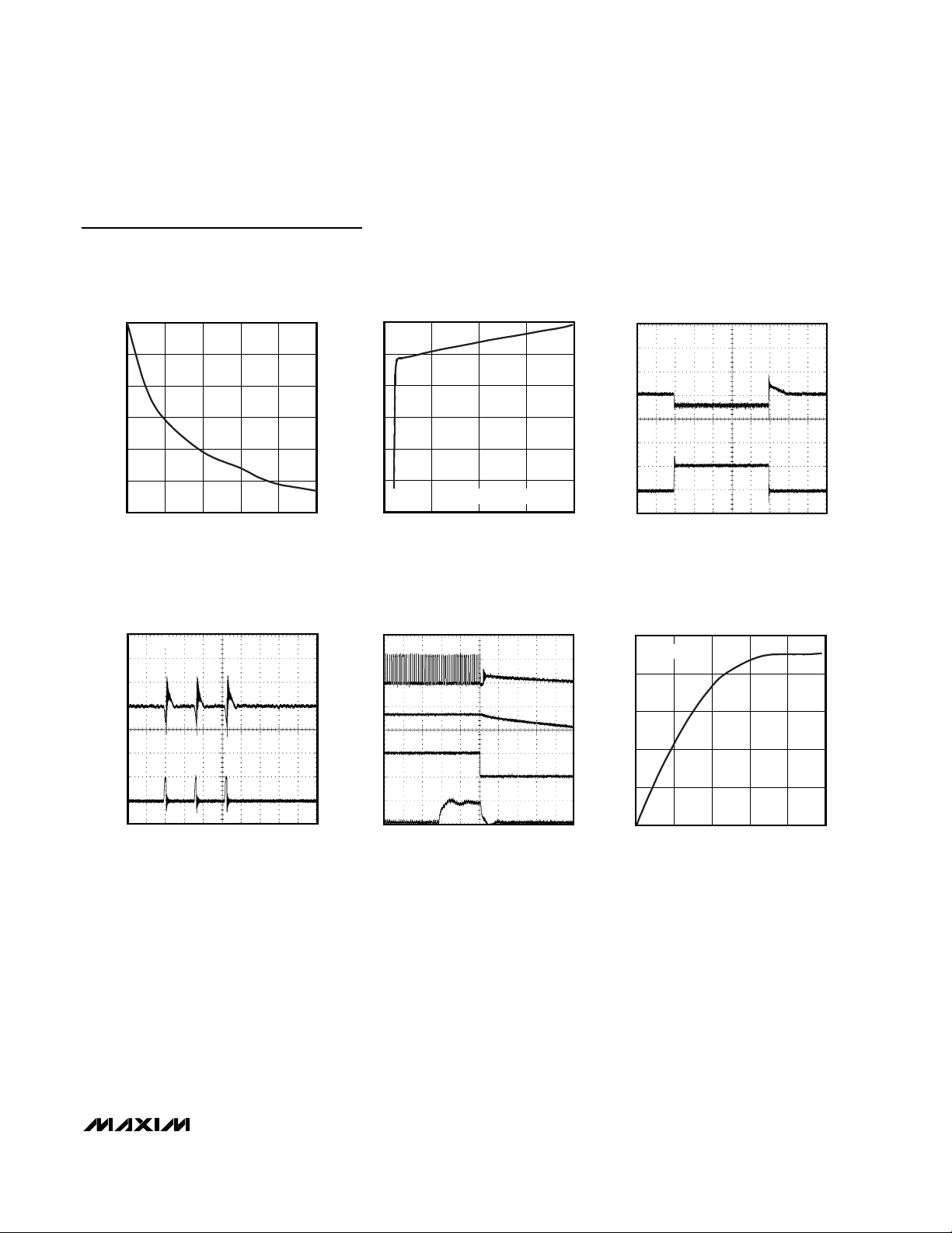
Typical Operating Characteristics
(Circuit of Figure 1; including R5, R6, and D2; TA= +25°C, unless otherwise noted.)
STEP-DOWN EFFICIENCY vs. LOAD CURRENT
MAX1530 toc01
LOAD CURRENT (mA)
EFFICIENCY (%)
1200900600300
60
70
80
90
100
50
0 1500
VIN = 12V
VIN = 20V
fSW = 500kHz
STEP-DOWN LOAD REGULATION
MAX1530 toc02
LOAD CURRENT (mA)
OUTPUT-VOLTAGE ERROR (%)
1200900600300
-0.12
-0.08
-0.04
0
-0.16
0 1500
SWITCHING FREQUENCY vs. LOAD CURRENT
FREQUENCY (kHz)
485
490
495
500
510
505
515
520
480
MAX1530 toc03
LOAD CURRENT (mA)
12009006003000 1500
STEP-DOWN REGULATOR LOAD TRANSIENT
MAX1530 toc04
40µs/div
A: LOAD CURRENT, 1A/div
B: OUTPUT VOLTAGE, 200mV/div, AC-COUPLED
C: INDUCTOR CURRENT, 1A/div
A
0A
B
3.3V
0A
C
STEP-DOWN REGULATOR
SWITCHING WAVEFORM
MAX1530 toc05
2µs/div
A
B
C
A: LX, 10V/div
B: OUTPUT VOLTAGE, 20 mV/div, AC-COUPLED
C: INDUCTOR CURRENT, 1A/div
0V
3.3V
0A
STEP-DOWN REGULATOR
SOFT-START
MAX1530 toc06
1ms/div
A
C
A: EN, 2V/div
B: OUTPUT VOLTAGE, 2V/div
C: INDUCTOR CURRENT, 1A/div
0V
0V
B
0A
VL LOAD REGULATION
MAX1530 toc07
LOAD CURRENT (mA)
VL OUTPUT ERROR (%)
252015105
-0.4
-0.3
-0.2
-0.1
0
-0.5
030
STARTUP SEQUENCE
MAX1530 toc08
4ms/div
A: V
L
, 10V/div
B: V
OUT
, 5V/div
C: V
LOGIC
, 5V/div
D: V
SOURCE
, 20V/div
E: V
GAMMA
, 20V/div
F: V
GOFF
, 20V/div
G: V
GON
, 40V/div
A
B
C
D
E
F
G
LR1 BASE CURRENT
vs. DRV1 VOLTAGE
MAX1530 toc09
DRV1 VOLTAGE (V)
BASE CURRENT (mA)
8642
3
6
9
12
15
0
010
V
FBL1
= 1.175V
Page 8
MAX1530/MAX1531
Multiple-Output Power-Supply Controllers for
LCD Monitors
8 _______________________________________________________________________________________
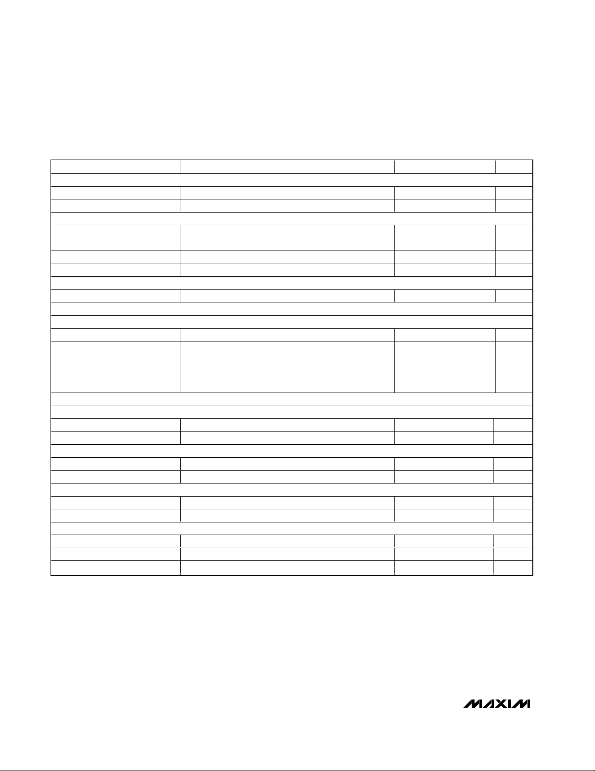
Typical Operating Characteristics (continued)
(Circuit of Figure 1; including R5, R6, and D2; TA= +25°C, unless otherwise noted.)
LR1 NORMALIZED LOAD REGULATION
0
LR1 NORMALIZED LINE REGULATION
0.2
LR1 LOAD TRANSIENT
MAX1530 toc12
-0.5
-1.0
VOLTAGE ERROR (%)
-1.5
-2.0
0 500
LOAD CURRENT (mA)
400300200100
MAX1530 toc10
OUTPUT-VOLTAGE ERROR (%)
LR2/LR3 BASE CURRENT
5
4
3
2
BASE CURRENT (mA)
1
0
vs. DRV2/DRV3 VOLTAGE
V
= V
FBL2
05
= 1.175V
FBL3
DRV2/DRV3 VOLTAGE (V)
MAX1530 toc13
VOLTAGE ERROR (%)
4321
0
-0.2
-0.4
-0.6
-0.8
-1.0
26
200mA LOAD CURRENT
543
INPUT VOLTAGE (V)
LR2 NORMALIZED LOAD REGULATION
0
-0.3
-0.6
-0.9
-1.2
-1.5
050
LOAD CURRENT (mA)
40302010
MAX1530 toc11
A: LR1 OUTPUT VOLTAGE, 100mV/div, AC-COUPLED
B: LR1 LOAD CURRENT, 500mA/div
LR2 NORMALIZED LINE REGULATION
0.2
0
MAX1530 toc14
-0.2
-0.4
-0.6
OUTPUT-VOLTAGE ERROR (%)
-0.8
-1.0
925
INPUT VOLTAGE (V)
A
2.5V
B
0mA
40µs/div
MAX1530 toc15
20mA LOAD CURRENT
211713
LR3 NORMALIZED LOAD REGULATION
0
-0.5
-1.0
VOLTAGE ERROR (%)
-1.5
-2.0
020
LOAD CURRENT (mA)
161284
MAX1530 toc16
LR3 NORMALIZED LINE REGULATION
0.2
0
-0.2
-0.4
-0.6
OUTPUT-VOLTAGE ERROR (%)
-0.8
-1.0
24 40
20mA LOAD CURRENT
INPUT VOLTAGE (V)
vs. DRV VOLTAGE
30
V
= 1.175V
FBL4
25
MAX1530 toc17
20
15
10
BASE CURRENT (mA)
5
363228
0
010
DRV4 VOLTAGE (V)
LR4 BASE CURRENT
MAX1530 toc18
8642
Page 9
MAX1530/MAX1531
Multiple-Output Power-Supply Controllers for
LCD Monitors
_______________________________________________________________________________________ 9
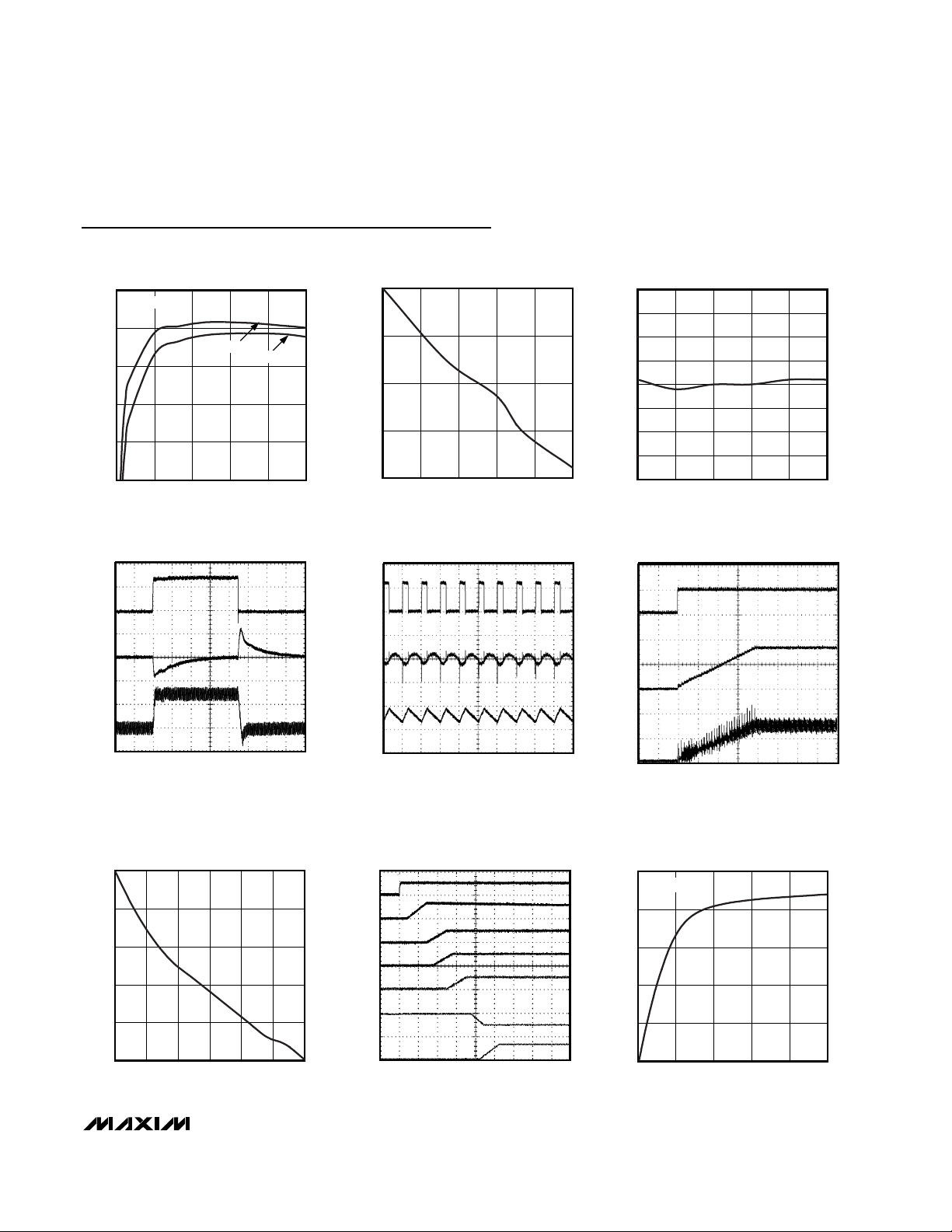
Typical Operating Characteristics (continued)
(Circuit of Figure 1; including R5, R6, and D2; TA= +25°C, unless otherwise noted.)
LR4 NORMALIZED LOAD REGULATION
MAX1530 toc19
LOAD CURRENT (mA)
VOLTAGE ERROR (%)
400300200100
-0.5
-0.4
-0.3
-0.2
-0.1
0
-0.6
0 500
LR4 NORMALIZED LINE REGULATION
MAX1530 toc20
INPUT VOLTAGE (V)
OUTPUT-VOLTAGE ERROR (%)
211713
-0.8
-0.6
-0.4
-0.2
0
0.2
-1.0
925
200mA LOAD CURRENT
LR4 LOAD TRANSIENT
MAX1530 toc21
40µs/div
A
B
A: LR4 OUTPUT VOLTAGE, 100mV/div, AC-COUPLED
B: LR4 LOAD CURRENT, 500mA/div
10V
0mA
LR4 PULSED LOAD TRANSIENT
MAX1530 toc22
10µs/div
A
B
A: LR4 OUTPUT VOLTAGE, 100mV/div, AC-COUPLED
B: LR4 LOAD CURRENT, 1A/div
10V
0A
MAX1531
OVERCURRENT PROTECTION (CSH, CSL)
MAX1530 toc23
20µs/div
A: V
LX
, 10V/div
B: V
OUT
, 5V/div
B
C
D
A
C: V
RESET
, 5V/div
D: V
CSH
- V
CSL
, 500mV/div
LR5 BASE CURRENT
vs. DRV5 VOLTAGE
MAX1530 toc24
DRV5 VOLTAGE (V)
BASE CURRENT (mA)
4321
2
4
6
8
10
0
05
V
FBL5
= 0V
Page 10
MAX1530/MAX1531
Multiple-Output Power-Supply Controllers for
LCD Monitors
10 ______________________________________________________________________________________
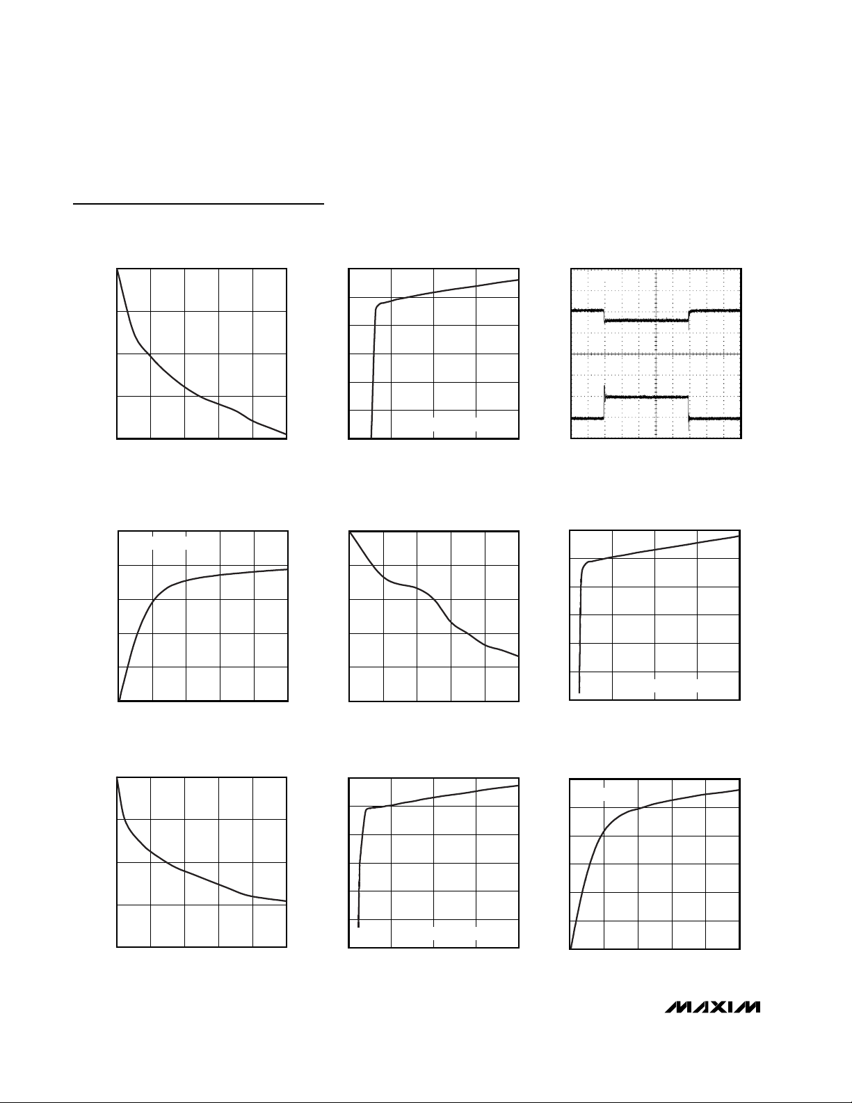
Typical Operating Characteristics (continued)
(Circuit of Figure 1; including R5, R6, and D2; TA= +25°C, unless otherwise noted.)
Pin Description
LR5 NORMALIZED LOAD REGULATION
0
-0.2
-0.4
-0.6
VOLTAGE ERROR (%)
-0.8
-1.0
050
LOAD CURRENT (mA)
40302010
PIN
MAX1530 MAX1531
1 1 DRV2
2 2 FBL2
NAME FUNCTION
Gamma Linear Regulator (LR2) Base Drive. Open drain of an internal N-channel MOSFET.
Connect DRV2 to the base of an external PNP pass transistor to form a positive linear
regulator. (See the Pass Transistor Selection section.)
Gamma Linear Regulator (LR2) Feedback Input. FBL2 regulates at 1.245V nominal.
Connect FBL2 to the center tap of a resistive voltage-divider between the LR2 output and
AGND to set the output voltage. Place the divider close to the FBL2 pin.
MAX1530 toc25
LR5 NORMALIZED LINE REGULATION
1.0
20mA LOAD CURRENT
0.8
0.6
0.4
0.2
OUTPUT-VOLTAGE ERROR (%)
0
-0.2
-25 -9
INPUT VOLTAGE (V)
MAX1530 toc26
-13-17-21
Gate-On Linear Regulator (LR3) Feedback Input. FBL3 regulates at 1.245V nominal.
3 3 FBL3
4 4 DRV3
Connect FBL3 to the center tap of a resistive voltage-divider between the LR3 output and
AGND to set the output voltage. Place the divider close to the FBL3 pin.
Gate-On Linear Regulator (LR3) Base Drive. Open drain of an internal N-channel MOSFET.
Connect DRV3 to the base of an external PNP pass transistor to form a positive linear
regulator. (See the Pass Transistor Selection section.)
5–10, 18, 19 — N. C. No Connection. Not internally connected.
Adjustable Reset Input. RESET asserts low when the monitored voltage is less than the
reset trip threshold. RESET goes to a high-impedance state only after the monitored
voltage remains above the reset trip threshold for the duration of the reset timeout period.
11 11 RSTIN
Connect RSTIN to the center tap of a resistive voltage-divider between the monitored
output voltage and AGND to set the reset trip threshold. The internal RSTIN threshold of
90% of 1.238V allows direct connection of RSTIN to any of the device’s positive feedback
pins.
Page 11

MAX1530/MAX1531
Multiple-Output Power-Supply Controllers for
LCD Monitors
______________________________________________________________________________________ 11
Pin Description (continued)
PIN
MAX1530 MAX1531
12 12 RESET
13 13 COMP
14 14 FB
15 15 ILIM
16 16 ONL2
NAME FUNCTION
Open-Drain Reset Output. RESET asserts low when the monitored voltage is less than the
reset trip threshold. RESET goes to a high-impedance state only after the monitored
voltage remains above the reset trip threshold for the duration of the reset timeout period.
RESET also asserts low when VL is less than the VL undervoltage lockout threshold, EN is
low, or the thermal, overcurrent or undervoltage fault latches are set.
Step-Down Regulator Compensation Input. A pole-zero pair must be added to
compensate the control loop by connecting a series resistor and capacitor from COMP to
AGND. (See the Compensation Design section.)
Step-Down Regulator Feedback Input. FB regulates at 1.238V nominal. Connect FB to the
center tap of a resistive voltage-divider between the step-down regulator output and
AGND to set the output voltage. Place the divider close to the FB pin.
Step-Down Regulator Current-Limit Control Input. Connect this dual-mode input to VL to
set the current-limit threshold to its default value of 250mV. The overcurrent comparator
compares the voltage across the low-side N-channel MOSFET with the current-limit
threshold. Connect ILIM to the center tap of a resistive voltage-divider between VL and
AGND to adjust the current-limit threshold to other values. In adjustable mode, the actual
current-limit threshold is 1/5th of the voltage at ILIM over a 0.25V to 3.0V range. The dualmode threshold for switchover to the 250mV default value is approximately 3.5V.
Gamma Linear Regulator (LR2) Enable Input. When EN is above its enable threshold, VL
is above its UVLO threshold, and ONL2 is greater than the internal reference, LR2 is
enabled. Drive ONL2 with a logic signal or, for automatic sequencing, connect a capacitor
from ONL2 to AGND. If SEQ is high, EN is above its threshold, and VL is above its UVLO
threshold, an internal 2µA (typ) current source charges the capacitor. Otherwise, an
internal switch discharges the capacitor. Connecting various capacitors to each ONL_ pin
allows the programming of the startup sequence.
Gate-On Linear Regulator (LR3) Enable Input. When EN is above its enable threshold, VL
is above its UVLO threshold, and ONL3 is greater than the internal reference, LR3 is
enabled. Drive ONL3 with a logic signal or, for automatic sequencing, connect a capacitor
17 17 ONL3
from ONL3 to AGND. If SEQ is high, EN is above its threshold, and VL is above its UVLO
threshold, an internal 2µA (typ) current source charges the capacitor. Otherwise, an
internal switch discharges the capacitor. Connecting various capacitors to each ONL_ pin
allows the programming of the startup sequence.
20 20 PGND Power Ground
Low-Side Gate Driver Output. DL drives the synchronous rectifier of the step-down
21 21 DL
22 22 LX
regulator. DL swings from PGND to VL. DL remains low until VL rises above the UVLO
threshold.
Step-Down Regulator Current-Sense Input. The IC’s current-sense amplifier inputs for
current-mode control connect to IN and LX. Connect IN and LX directly to the high-side Nchannel MOSFET drain and source, respectively. The low-side current-limit comparator
inputs connect to LX and PGND to sense voltage across a low-side N-channel MOSFET.
Page 12

MAX1530/MAX1531
Multiple-Output Power-Supply Controllers for
LCD Monitors
12 ______________________________________________________________________________________
Pin Description (continued)
PIN
MAX1530 MAX1531
23 23 DH
24 24 BST
25 25 SEQ
26 26 FREQ
NAME FUNCTION
High-Side Gate Driver Output. DH drives the main switch of the step-down regulator. DH
swings from LX to BST.
Step-Down Regulator Boostrap Capacitor Connection for High-Side Gate Driver. Connect
a 0.1µF ceramic capacitor from BST to LX.
Sequence Control Input for LR2, LR3, LR4, and LR5. Controls the current sources and
switches that charge and discharge the capacitors connected to the ONL_ pins.
Oscillator Frequency Select Input. Connect FREQ to VL for 500kHz operation. Connect
FREQ to AGND for 250kHz operation.
Main Input Voltage (+4.5V to 28V). Bypass IN to AGND with a 1µF ceramic capacitor
27 27 IN
close to the pins. IN powers the VL linear regulator. Connect IN to the drain of the highside MOSFET (for current sense) through a 1Ω resistor.
Internal 5V Linear Regulator Output. Connect a minimum 1µF ceramic capacitor from VL
28 28 VL
to AGND. Place the capacitor close to the pins. VL can supply up to 30mA for gate drive
and external loads. VL remains active when EN is low.
29 29 AGND Analog Ground
Enable Input. This general-purpose on/off control input has an accurate 1.238V (typ) rising
threshold with 5% hysteresis. This allows EN to monitor an input voltage level or other
analog parameter. If EN is less than its threshold, then the main step-down and all linear
30 30 EN
regulators are turned off. VL and the internal reference remain active when EN is low. The
rising edge of EN clears any latched faults except for a thermal fault, which is cleared only
by cycling the input power. An internal filter with a 10µs time constant prevents short
glitches from accidentally clearing the fault latch.
Low-Voltage Logic Linear Regulator (LR1) Feedback Input. FBL1 regulates at 1.245V
31 31 FBL1
32 32 DRV1
— 5 CSH
nominal. Connect FBL1 to the center tap of a resistive voltage-divider between LR1 output
AGND to set the output voltage. Place the divider close to the FBL1 pin. LR1 starts
automatically after the step-down converter soft-start ends.
Low-Voltage Logic Linear Regulator (LR1) Base Drive. Open drain of an internal N-channel
MOSFET. Connect DRV1 to the base of an external PNP pass transistor. (See the Pass
Transistor Selection section.)
Overcurrent Protection Positive Input. CSH is also the supply input for the overcurrent
sense block. CSH and CSL can be used to sense any current in the application circuit and
to shut the device down in an overcurrent condition. This feature is typically used to
protect the main input or the input to one of the linear regulators since they do not have
their own current limits. Insert an appropriate sense resistor in series with the protected
input and connect CSH and CSL to its positive and negative terminals. The controller sets
the fault latch when V
internal lowpass filter prevents large currents of short duration (less than 50µs) or noise
glitches from setting the latch. If the overcurrent protection is not used, connect CSH and
CSL to VL.
CSH
- V
exceeds the 300mV (typ) overcurrent threshold. An
CSL
— 6 CSL Overcurrent Protection Negative Input. See CSH above.
Page 13

MAX1530/MAX1531
Multiple-Output Power-Supply Controllers for
LCD Monitors
______________________________________________________________________________________ 13
Pin Description (continued)
PIN
MAX1530 MAX1531
— 7 FBL4
— 8 DRV4
— 9 FBL5
— 10 DRV5
— 18 ONL4
NAME FUNCTION
Source Drive Linear Regulator (LR4) Feedback Input. FBL4 regulates at 1.245V nominal.
Connect FBL4 to the center tap of a resistive voltage-divider between the LR4 output and
AGND to set the output voltage. Place the divider close to the FBL4 pin.
Source Drive Linear Regulator (LR4) Base Drive. Open drain of an internal N-channel
MOSFET. Connect DRV4 to the base of an external PNP pass transistor to form a positive
linear regulator. (See the Pass Transistor Selection section.)
Gate-Off Linear Regulator (LR5) Feedback Input. FBL5 regulates at 125mV nominal.
Connect FBL5 to the center tap of a resistive voltage-divider between the LR5 output and
the internal 5V linear regulator output (VL) to set the output voltage. Place the divider close
to the FBL5 pin.
Gate-Off Linear Regulator (LR5) Base Drive. Open drain of an internal P-channel MOSFET.
Connect DRV5 to the base of an external NPN pass transistor to form a negative linear
voltage regulator. (See the Pass Transistor Selection section.)
Source Drive Linear Regulator (LR4) Enable Input. When EN is above its enable threshold,
VL is above its UVLO threshold, and ONL4 is greater than the internal reference, LR4 is
enabled. Drive ONL4 with a logic signal or, for automatic sequencing, connect a capacitor
from ONL4 to AGND. If SEQ is high, EN is above its threshold, and VL is above its UVLO
threshold, an internal 2µA (typ) current source charges the capacitor. Otherwise, an
internal switch discharges the capacitor. Connecting various capacitors to each ONL_ pin
allows the programming of the startup sequence.
— 19 ONL5
Gate-Off Linear Regulator (LR5) Enable Input. When EN is above its enable threshold, VL
is above its UVLO threshold, and ONL5 is greater than the internal reference, LR5 is
enabled. Drive ONL5 with a logic signal or, for automatic sequencing, connect a capacitor
from ONL5 to AGND. If SEQ is high, EN is above its threshold, and VL is above its UVLO
threshold, an internal 2µA (typ) current source charges the capacitor. Otherwise, an
internal switch discharges the capacitor. Connecting various capacitors to each ONL_ pin
allows the programming of the startup sequence.
Page 14
MAX1530/MAX1531
Multiple-Output Power-Supply Controllers for
LCD Monitors
14 ______________________________________________________________________________________
Figure 1. MAX1531 Standard Application Circuit
= 12V
V
IN
C3
4.7µF
25V
20.0kΩ
V
L
5V/30mA
C20
0.1µF
V
GAMMA
9.7V/50mA
2.2µF
V
SOURCE
10V/500mA
C21
C13
4.7µF
16V
Q2
Q4
R3
124kΩ
1%
R4
1%
C4
1µF
R7
100kΩ
R14
121kΩ
1%
R15
68.1kΩ
1%
R16
43.2kΩ
1%
C11
0.1µF
R17
V
IN
6.8kΩ
R18
68.1kΩ
1%
C12
0.47µF
R20
0.5Ω
1%
75kΩ
R22
1%
R21
1.5kΩ
R19
10kΩ
1%
V
IN
R23
10.7kΩ
1%
D1
R5*
10Ω
24
30
EN IN
28
VL
26
FREQ
25
SEQ
12
RESET
16
ONL2
17
ONL3
18
ONL4
19
ONL5
1
DRV2
2
FBL2
6
CSL
5
CSH
8
DRV4
7
BST
MAX1531
PGND
AGND
DRV1
FBL1
RSTIN
COMP
ILIM
DRV3
FBL3
DRV5
FBL5FBL4
C5
0.1µF
IN
R12
IN
0.1µF
Q6
C14
LX
C1
1µF
10Ω
D2*
R6*
1Ω
N1-A
L1
10µH
C7
22µF
N1-B
R8
6.8kΩ
R26
1%
D4
C6
0.1µF
D5
R28
90.9kΩ
1%
*OPTIONAL
R9
10kΩ
1%
C10
470pF
C2, OPEN
R25
200kΩ
1%
D6
R24
6.8kΩ
R27
6.8kΩ
R10
10kΩ
1%
R11
100kΩ
D3
C8
0.1µF
IN
10.5kΩ
C17
0.1µF
LX
R29
48.7kΩ
1%
VL
6.3V
C22
2.2µF
Q1
C9
10µF
6.3V
C15
0.1µF
Q3
C16
0.47µF
C18
0.1µF
Q5
C19
0.47µF
27
23
DH
22
LX
21
DL
20
29
32
31
11
14
FB
13
15
V
4
3
10
9
C23
150pF
VL
R12
300kΩ
R13
150kΩ
V
OUT
3.3V/1.5A
R1
17.8kΩ
1%
R2
10.7kΩ
1%
V
LOGIC
2.5V/500mA
V
GON
25V/20mA
V
GOFF
-9V/50mA
Page 15

MAX1530/MAX1531
Multiple-Output Power-Supply Controllers for
LCD Monitors
______________________________________________________________________________________ 15
Figure 2. MAX1530 Standard Application Circuit
V
= 12V
IN
C3
V
L
5V/30mA
C20
0.1µF
V
GAMMA
9.7V/50mA
4.7µF
25V
R4
20.0kΩ
1%
V
Q2
R3
124kΩ
1%
C4
1µF
R7
100kΩ
R14
121kΩ
1%
C11
0.1µF
R17
IN
6.8kΩ
R18
68.1kΩ
1%
C12
0.47µF
R19
10kΩ
1%
D1
R5*
10Ω
24
30
EN IN
28
VL
26
FREQ
25
SEQ
12
RESET
16
ONL2
17
ONL3
5
N.C.
6
N.C.
7
N.C.
8
N.C.
1
DRV2
2
FBL2
9
N.C.
10
N.C.
BST
MAX1530
PGND
AGND
DRV1
FBL1
RSTIN
COMP
ILIM
DRV3
FBL3
N.C.
N.C.
C5
0.1µF
IN
R12
C1
1µF
R6*
10Ω
D2*
1Ω
N1-A
L1
10µH
C7
C23
22µF
150pF
6.3V
C22
2.2µF
Q1
C9
10µF
6.3V
VL
R12
300kΩ
R13
C21
2.2µF
Q4
C13
4.7µF
150kΩ
R11
100kΩ
R23
10.7kΩ
N1-B
R8
6.8kΩ
R10
R9
10kΩ
10kΩ
1%
1%
C10
470pF
C2, OPEN
V
IN
R24
6.8kΩ
R22
75kΩ
1%
1%
27
23
DH
22
LX
21
DL
20
29
32
31
11
14
FB
13
15
4
3
19
18
3.3V/1.5A
R1
17.8kΩ
1%
R2
10.7kΩ
1%
2.5V/500mA
V
10V/500mA
V
OUT
V
LOGIC
SOURCE
*OPTIONAL
Page 16

MAX1530/MAX1531
Multiple-Output Power-Supply Controllers for
LCD Monitors
16 ______________________________________________________________________________________
Standard Application Circuit
The standard application circuit (Figure 1) of the
MAX1531 is a complete power-supply system for TFT
LCD monitors. The circuit generates a 3.3V/1.5A main
output, a 2.5V/500mA output for the timing controller
and digital sections of source/gate drive ICs, a
10V/500mA source drive supply voltage, a 9.7V/50mA
gamma reference, a 25V/20mA gate-on voltage, and a
-10V/50mA gate-off voltage. The input voltage is 12V
±10%. Table 1 lists the selected components and Table
2 lists the component suppliers. The standard application circuit (Figure 2) of the MAX1530 is similar to the
MAX1531 application circuit except that gate-on and
gate-off voltages are eliminated.
Detailed Description
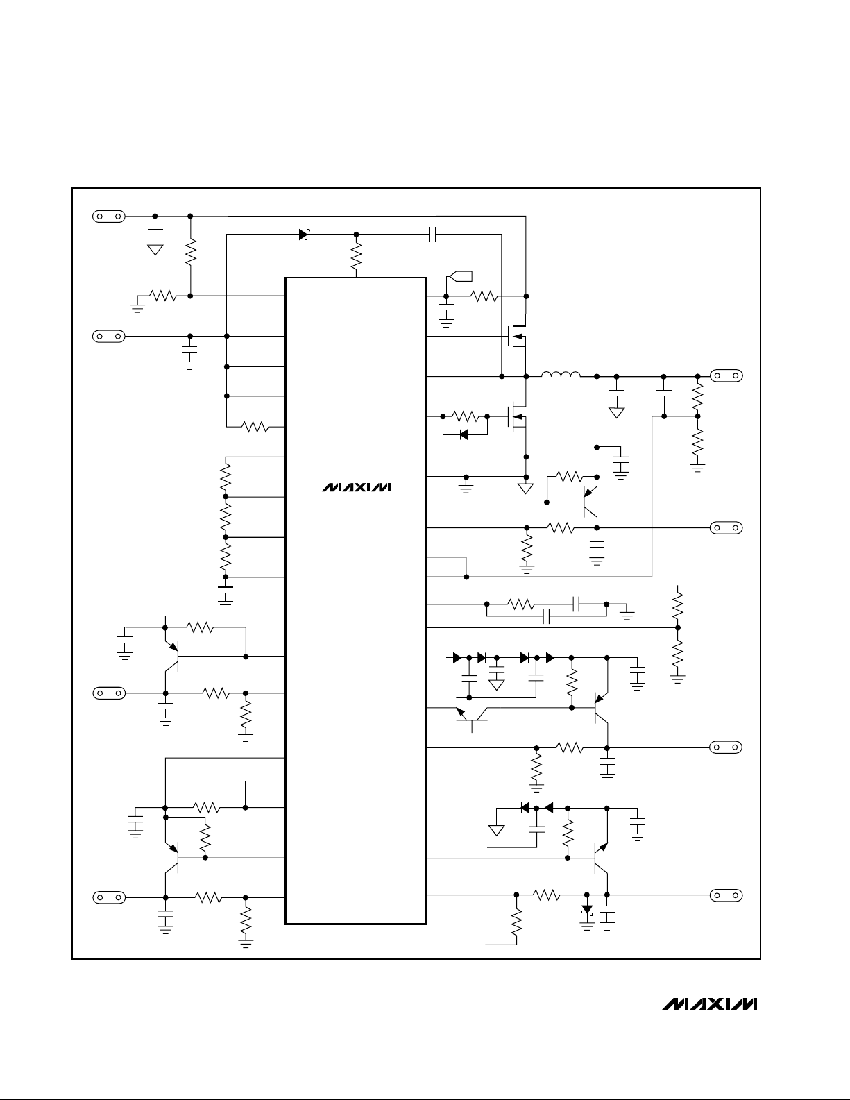
The MAX1530/MAX1531 power-supply controllers provide logic and bias power for LCD monitors. Figure 3
shows the IC functional diagram. The main step-down
controller employs a current-mode PWM control method
to ease compensation requirements and provide excellent load- and line-transient response. The use of synchronous rectification yields excellent efficiency.
The MAX1530 includes three analog gain blocks to
control three auxiliary positive linear regulators, and the
MAX1531 includes five analog gain blocks to control
four positive and one negative linear regulators. Use
the positive gain blocks to generate low-voltage rails
directly from the input voltage or the main step-down
converter output, or higher voltages using charge
Table 1. Selected Component List
Table 2. Component Suppliers
*For MAX1531 only.
DESIGNATION DESCRIPTION
C3
C7
C9
C12, C19*
C13
C21, C22
D1, D6*
D2
SUPPLIER PHONE FAX WEBSITE
Central Semi 516-435-1110 516-435-1824 www.centralsemi.com
Fairchild 888-522-5372 972-910-8036 www.fairchildsemi.com
Sumida 847-956-0666 847-956-0702 www.sumida.com
TDK 847-803-6100 847-390-4405 www.components.tdk.com
4.7µF, 25V X7R ceramic capacitor (1210)
TDK C3225X7R1E475K
22µF, 6.3V X7R ceramic capacitor
TDK C3216X7R0J226M
10µF, 6.3V X5R ceramic capacitor
TDK C2012X5R0J106M
0.47µF, 16V X7R ceramic capacitors (0805)
TDK C2012X7R1C474K
4.7µF, 16V X7R ceramic capacitor
TDK C3216X7R1C475K
2.2µF, 25V X7R ceramic capacitors (1206)
TDK C3216X7R1C475M
100mA, 30V Schottky diodes (SOD523)
Central Semiconductor CMOSH-3
100mA, 75V, small-signal switching diode,
SOT23 Fairchild Semiconductor MMBD4148
DESIGNATION DESCRIPTION
D3*, D4*, D5*
L1
N1
Q1, Q4
Q2, Q3*
Q5*, Q6*
200mA, 25V dual Schottky diodes (SOT23)
Fairchild BAT54S
10µH, 2.3A (DC) inductor
Sumida CDR7D28MN-100
2.5A, 30V dual N-channel MOSFET (6-pin
Super SOT)
Fairchild FDC6561AN
3A, 60V l ow - satur ati on P N P b i p ol ar tr ansi stor s
( S O T- 223)
Fai r chi l d N Z T660A
200mA, 40V PNP bipolar transistors (SOT23)
Fairchild MMBT3906
200m A, 40V N P N b i p ol ar tr ansi st or s ( S OT23)
Fai r chi l d M M BT3904
Page 17

MAX1530/MAX1531
Multiple-Output Power-Supply Controllers for
LCD Monitors
______________________________________________________________________________________ 17
Figure 3. IC Functional Diagram
FREQ
EN
RSTIN
RESET
GND
COMP
FB
ILIM
ONL2
ONL3
ONL4
ONL5
SEQ
DRV1
V
REF
FBL1
CSH
CSL
DRV2 DRV5
300mV
VLOK
TIMER
COMP
FB
ILIM
PGND
SEQUENCE
SOFTSTART
LR1
0.9VREF
OSC REF
SLOPECLOCK
STEP-DOWN
CONTROLLER
SS DONE FLTMDC-DC EN
ON2
ON3
ON4
ON5
SEQ
EN
FLT1
FLTCS
IN
FAULT
LOGIC
DH
LX
DL
FLTM
FLT3
LDO3EN
LDO4EN
FLT4
V
REF
HIGH-SIDE
DRIVER
LOW-SIDE
DRIVER
THERMAL
VL
VL
MAX1531
SOFTSTART
LR3
0.9VREF
SOFT-
START
LR4
0.9VREF
IN
VL
BST
DH
LX
DL
PGND
DRV3
V
REF
FBL3
DRV4
V
REF
FBL4
V
REF
FBL2 FBL5
SOFTSTART
LR2
0.9VREF
LDO2EN LDO5EN
FLT5FLT2
VLOKEN
SOFT-
START
400mV
LR5
V
REF
Page 18

MAX1530/MAX1531
Multiple-Output Power-Supply Controllers for
LCD Monitors
18 ______________________________________________________________________________________
pumps attached to the switching node or extra windings coupled to the step-down converter inductor. The
negative gain block (MAX1531) can be used in conjunction with a charge pump or coupled winding to
generate the LCD gate-off voltage or other negative
supplies.
Step-Down Controller
The MAX1530/MAX1531 include step-down controllers
that use a fixed-frequency current-mode PWM control
scheme (Figure 4). An internal transconductance
amplifier establishes an integrated error voltage at the
COMP pin. The heart of the current-mode PWM controller is an open-loop comparator that compares an
integrated voltage-feedback signal with an amplified
current-sense signal plus a slope-compensation ramp.
At each rising edge of the internal clock, the high-side
MOSFET turns on until the PWM comparator trips or the
maximum duty cycle is reached. During this on-time,
current ramps up through the inductor, sourcing current to the output and storing energy in a magnetic
field. The current-mode feedback system regulates the
peak inductor current as a function of the output voltage error signal. Since the average inductor current is
nearly the same as the peak inductor current (assuming that the inductor value is relatively high to minimize
ripple current), the circuit acts as a switch-mode
transconductance amplifier. That pushes the output LC
filter pole, normally found in a voltage-mode PWM, to a
higher frequency. To preserve loop stability, the slopecompensation ramp is summed into the main PWM
comparator.
During the second half of the cycle, the high-side MOSFET turns off and the low-side N-channel MOSFET turns
on. Now the inductor releases the stored energy as its
current ramps down, providing current to the output.
The output capacitor stores charge when the inductor
current exceeds the load current and discharges when
the inductor current is lower, smoothing the voltage
across the load. Under overload conditions, when the
inductor current exceeds the selected current limit (see
Current Limit Circuit), the high-side MOSFET is not
turned on at the rising edge of the clock and the lowside MOSFET remains on to let the inductor current
ramp down.
Under light-load conditions, the MAX1530/MAX1531
maintain a constant switching frequency to minimize
cross-regulation errors in applications that use a transformer. The low-side gate-drive waveform is the complement of the high-side gate-drive waveform, which
causes the inductor current to reverse under light loads.
Current-Sense Amplifier
The MAX1530/MAX1531s’ current-sense circuit amplifies the current-sense voltage generated by the highside MOSFET’s on-resistance. This amplified
current-sense signal and the internal slope compensation signal are summed together and fed into the PWM
comparator’s inverting input. Place the high-side MOSFET near the controller, and connect IN and LX to the
MOSFET using Kelvin-sense connections to guarantee
current-sense accuracy and improve stability.
Current-Limit Circuit
The MAX1530/MAX1531 include two current-limit circuits that use the two MOSFETs’ on-resistances as current-sensing elements (Figure 4). The high-side
MOSFET’s voltage is used with a fixed 400mV (typ) current-limit threshold during the high-side on-times. The
low-side MOSFET’s voltage is used with an adjustable
current-limit threshold during the low-side on-times.
Using both circuits together ensures that the current is
always measured and controlled.
The high-side MOSFET current limit employs a peak
current limit. If the voltage across the high-side MOSFET, measured from IN to LX, exceeds the 400mV
threshold during an on-time, the high-side MOSFET
turns off and the low-side MOSFET turns on.
The low-side MOSFET current-limit circuit employs a
“valley” current limit. If the voltage across the low-side
MOSFET, measured from LX to PGND, exceeds the
low-side threshold at the end of a low-side on-time, the
low-side MOSFET remains on and the high-side MOSFET stays off for the entire next cycle.
Figure 4. Step-Down Controller Block Diagram
CURRENT
SLOPE
SS DONE
DC-DC EN
V
REF
COMP
CLOCK
ILIM
SOFTSTART
FB
GM
0.9VREF
∑
CURRENT
SENSE
AND
CURRENT
LIMIT
PWM COMP
LIMIT
FAULT COMPARATOR
RSQ
Q
IN
DH
DL
LX
PGND
FLTM
Page 19

MAX1530/MAX1531
Multiple-Output Power-Supply Controllers for
LCD Monitors
______________________________________________________________________________________ 19
The ILIM pin is a dual-mode input. When ILIM is connected to VL, a default low-side current limit of 250mV
(typ) is used. If ILIM is connected to a voltage between
250mV and 3V, the low-side current limit is typically
1/5th the ILIM voltage.
The MAX1530/MAX1531s’ current limits are comparatively inaccurate, since the maximum load current is a
function of the MOSFETs’ on-resistances and the inductor value, as well as the accuracy of the two thresholds.
However, using MOSFET current sensing reduces both
cost and circuit size and increases efficiency, since
sense resistors are not needed.
MOSFET Gate Drivers (DH, DL)
The DH and DL drivers are optimized for driving moderate-size high-side and low-side MOSFETs. Adaptive
dead-time circuits monitor the DL and DH drivers and
prevent either FET from turning on until the other is fully
off. This algorithm allows operation without shootthrough with a wide range of MOSFETs, minimizing
delays and maintaining efficiency. When the gates are
turning off, there must be low-resistance, low-inductance paths from the gate drivers to the MOSFET gates
for the adaptive dead-time circuit to work properly.
Otherwise, the sense circuitry in the MAX1530/
MAX1531 interpret the MOSFET gate as "off" while gate
charge actually remains. Use short, wide traces measuring less than 50 squares (at least 20 mil wide if the
MOSFET is 1in from the device).
It is advantageous to slow down the turn-on of both
gate drivers if there is noise coupling between the
switching regulator and the linear regulators. The noise
coupling can result in excessive switching ripple on the
linear regulator outputs. Slowing down the turn-on of
the gate drivers proves to be an effective way of reducing the output ripple. Take care to ensure that the turnoff times are not affected at the same time. As
explained above, slowing down the turn-off times may
result in shoot-through problems. In Figure 1, a 10Ω
resistor (R5) is inserted in series with the BST pin to
slow down the turn-on of the high-side MOSFET (N1-B)
without affecting the turn-off. A 10Ω resistor (R6) is also
inserted between DL and the gate of the low-side MOSFET (N1-A) to slow its turn-on. Because the gate resistor would slow down the turn-off time, connect a
switching diode (D2) (such as 1N4148) in parallel with
the gate resistor as shown in Figure 1 to prevent potential shoot-through.
High-Side Gate-Drive Supply (BST)
A flying-capacitor bootstrap circuit generates gatedrive voltage for the high-side N-channel switch (Figure
1). The capacitor C5 between BST and LX is alternately
charged from the VL supply and placed parallel to the
high-side MOSFET’s gate-source terminals.
On startup, the synchronous rectifier (low-side MOSFET) forces LX to ground and charges the boost
capacitor from VL through diode D1. On the second
half-cycle, the switch-mode power supply turns on the
high-side MOSFET by closing an internal switch
between BST and DH. This provides the necessary
gate-to-source voltage to turn on the high-side switch,
an action that boosts the 5V gate-drive signal above
the input voltage.
Oscillator Frequency Selection (FREQ)
The FREQ pin can be used to select the switching frequency of the step-down regulator. Connect FREQ to
VL for 500kHz operation. Connect FREQ to AGND for
250kHz operation. The 500kHz operation minimizes the
size of the inductor and capacitors. The 250kHz operation improves efficiency by 2% to 3%.
Linear Regulator Controllers
The MAX1530/MAX1531 include three positive linear
regulator controllers, LR1, LR2, and LR3. These linear
regulator controllers can be used with external pass
transistors to regulate supplies for TFT LCDs. The
MAX1531 includes an additional positive linear regulator controller (LR4) and a negative linear regulator controller (LR5).
Low-Voltage Logic Regulator Controller (LR1)
LR1 is an analog gain block with an open-drain Nchannel output. It drives an external PNP pass transistor with a 6.8kΩ base-to-emitter resistor. Its guaranteed
base drive sink current is at least 3mA. The regulator
including transistor Q1 in Figure 1 uses a 10µF output
capacitor and is designed to deliver 500mA at 2.5V.
LR1 is typically used to generate low-voltage logic supplies for the timing controller and the digital sections of
the TFT LCD source/gate driver ICs.
LR1 is enabled when the soft-start of the main stepdown regulator is complete. (See the Startup Sequence
(ONL_,SEQ) section.) Each time it is enabled, the controller goes through a soft-start routine that ramps up its
internal reference DAC. (See the Soft-Start section.)
Gamma Regulator Controller (LR2)
LR2 is an analog gain block with an open-drain Nchannel output. It drives an external PNP pass transistor with a 6.8kΩ base-to-emitter resistor. Its guaranteed
base drive sink current is at least 2mA. The regulator
including transistor Q2 in Figure 1 uses a 0.47µF output
capacitor and is designed to deliver 50mA at 9.7V.
Page 20

MAX1530/MAX1531
Multiple-Output Power-Supply Controllers for
LCD Monitors
20 ______________________________________________________________________________________
LR2 is typically used to generate the TFT LCD gamma
reference voltage, which is usually 0.3V below the
source drive supply voltage.
LR2 is enabled when the step-down regulator is
enabled and the voltage on ONL2 exceeds ONL2 input
threshold (1.238V typ). (See the Startup Sequence
(ONL_,SEQ) section.) Each time it is enabled, the controller goes through a soft-start routine that ramps up its
internal reference DAC. (See the Soft-Start section).
Linear Regulator Controller (LR3)
LR3 is an analog gain block with an open-drain Nchannel output. It drives an external PNP pass transistor with a 6.8kΩ base-to-emitter resistor. Its guaranteed
base drive sink current is at least 2mA. The regulator,
including Q3 in Figure 1, uses a 0.47µF output capacitor and is designed to deliver 20mA at 25V. The regulator including Q3 in Figure 2 uses a 4.7µF output
capacitor and is designed to deliver 500mA at 10V.
For the MAX1531 (Figure 1), LR3 is typically used to generate the TFT LCD gate driver’s gate-on voltage. A sufficient input voltage can be produced using a
charge-pump circuit as shown in Figure 1. Note that the
voltage rating of the DRV3 output is 28V. If higher voltages are present, an external cascode NPN transistor
(Q6) should be used with the emitter connected to
DRV3, the base to VIN(which is the connection point of
C1 and R12 in Figure 1), and the collector to the base of
the PNP pass transistor (Figure 1). For the MAX1530
(Figure 2), LR3 is typically used to generate the TFT LCD
source drive supply voltage. The input for this regulator
can come directly from the input supply, be produced
from an external step-up regulator, or from an extra winding coupled to the main step-down regulator inductor.
LR3 is enabled when the step-down regulator is
enabled and the voltage on ONL3 exceeds the ONL3
input threshold (1.238V typ). (See the Startup Sequence
(ONL_,SEQ) section.) Each time it is enabled, the controller goes through a soft-start routine that ramps up its
internal reference DAC. (See the Soft-Start section.)
Source Drive Regulator Controller (LR4)
(MAX1531 Only)
LR4 is an analog gain block with an open-drain Nchannel output. It drives an external PNP pass transistor with a 1.5kΩ base-to-emitter resistor. Its guaranteed
base drive sink current is at least 10mA. The regulator
including Q4 in Figure 1 uses a 4.7µF output capacitor
and is designed to deliver 500mA at 10V. The regulator’s fast transient response allows it to handle brief
peak currents up to 2A.
LR4 is typically used to generate the TFT LCD source
drive supply voltage. The input for this regulator can
come directly from the input supply, be produced from
an external step-up regulator, or from an extra winding
coupled to the main step-down regulator inductor.
LR4 is enabled when the step-down regulator is
enabled and the voltage on ONL4 exceeds the ONL4
input threshold (1.238V typ). (See the Startup
Sequence (ONL_,SEQ) section.) Each time it is
enabled, the regulator goes through a soft-start routine
that ramps up its internal reference DAC from 0V to
1.238V (typ). (See the Soft-Start section.)
The standard application circuit in Figure 1 powers the
LR4 regulator directly from the input supply and uses
the MAX1531’s general-purpose overcurrent protection
function to protect the input supply from excessive load
currents. (See the Overcurrent Protection section.)
Gate-Off Regulator Controller (LR5) (MAX1531 Only)
LR5 is an analog gain block with an open-drain P-channel output. It drives an external NPN pass transistor
with a 6.8kΩ base-to-emitter resistor. Its guaranteed
base drive sink current is at least 2mA. The regulator
including Q5 in Figure 1 uses a 0.47µF output capacitor
and is designed to deliver 10mA at -10V.
LR5 is typically used to generate the TFT LCD gate driver’s gate-off voltage. A negative input voltage can be
produced using a charge-pump circuit as shown in
Figure 1. Use as many stages as necessary to obtain
the required output voltage.
LR5 is enabled when the step-down regulator is
enabled and the voltage on ONL5 exceeds the ONL5
input threshold (1.238V typ). (See the Startup
Sequence (ONL_,SEQ) section.) Each time it is
enabled, the regulator goes through a soft-start routine
that ramps down its internal reference DAC from VL to
125mV (typ). (See the Soft-Start section.)
Internal 5V Linear Regulator (VL)
All MAX1530/MAX1531 functions, except the thermal
sensor, are internally powered from the on-chip, lowdropout 5V regulator. The maximum regulator input
voltage (VIN) is 28V. Bypass the regulator’s output (VL)
with at least a 1µF ceramic capacitor to AGND. The
VIN-to-VL dropout voltage is typically 200mV, so when
V
IN
is less than 5.2V, VL is typically VIN- 200mV. The
internal linear regulator can source up to 30mA to supply the device, power the low-side gate driver, charge
the external boost capacitor, and supply small external
loads. When driving particularly large MOSFETs, little or
no regulator current may be available for external
Page 21

MAX1530/MAX1531
Multiple-Output Power-Supply Controllers for
LCD Monitors
______________________________________________________________________________________ 21
loads. For example, when switched at 500kHz, large
MOSFETs with a total of 40nC total gate charge would
require 40nC × 500kHz, which is approximately 20mA.
On/Off Control (EN)
The EN pin has an accurate 1.238V (typ) rising threshold with 5% hysteresis. The accurate threshold allows it
to be used to monitor the input voltage or other analog
signals of interest. If VENvoltage is less than its threshold, then the step-down regulator and all linear regulators are turned off. VL and the internal reference remain
active when EN is low to allow an accurate EN threshold. A rising edge on the pin clears any latched faults
except for a thermal fault, which is cleared only by
cycling the input power.
Undervoltage Lockout
If VL drops below 3.4V (typ), the MAX1530/MAX1531
assume that the supply voltage is too low to make valid
decisions. Therefore, the undervoltage lockout (UVLO)
circuitry turns off all the internal bias supplies. Switching
is inhibited, and the DL and DH gate drivers are forced
low. After VL rises above 3.5V (typ), the fault and thermal
shutdown latches are cleared and startup begins if EN is
above its threshold.
Startup Sequence (ONL_, SEQ)
The MAX1530/MAX1531 are not enabled unless all four
of the following conditions are met: 1) VL exceeds the
UVLO threshold, 2) EN is above 1.238V, 3) the fault
latch is not set, and 4) the thermal shutdown latch is not
set. After all four conditions are met, the step-down controller starts switching and enables soft-start (Figure 5).
After the step-down regulator soft-start is done, the lowvoltage logic linear regulator controller (LR1) soft-starts.
The remaining linear regulator controllers and the
sequence block that can be used to control them are
enabled at the same time as the step-down regulator.
The SEQ logic input is used in combination with the
ONL_ pins to control the startup sequence. When SEQ
is high and the sequence block is enabled, each ONL_
pin sources 2µA (typ). When the voltage on an ONL_
pin reaches 1.238V (typ), its respective linear regulator
controller (LR_) is enabled. When SEQ is low or the
sequence block is not enabled, each ONL_ pin is connected to ground through a 1.5kΩ internal MOSFET.
The sequence block allows the user to program the
startup of LR2 to LR5 in any desired sequence. If no
capacitor is placed on an ONL_ pin, its LR_ controller
starts immediately after the sequence block is enabled
and SEQ goes high. Placing a 1.5nF capacitor on an
ONL_ pin provides about 1ms delay for the respective
LR_ controller. Placing different size capacitors on
each ONL_ pin allows any arbitrary startup sequence.
An arbitrary startup sequence can also be created with
a single capacitor (Figure 6). Capacitor C1, together
with the 8µA current (2µA per ONL_ pin), is chosen to
provide the desired delay for the controller that starts
last (ONLd). Using 0.1µF for C1 provides about 16ms
Figure 6. Single-Capacitor Sequence Configuration
Figure 5. Startup Conditions
EN > 1.24V
AND
STEP-DOWN
REGULATOR
STARTUP
STEP-DOWN
SOFT-START
LR1
STARTUP
DONE
VL > 3.5V
LR2
STARTUP
SEQUENCE
BLOCK
ENABLED
ONL3 > 1.24V
LR3
STARTUP
SEQ = HIGH
LR4
STARTUP
ONL_
CURRENT
SOURCES ON
ONL5 > 1.24VONL2 > 1.24V ONL4 > 1.24V
LR5
STARTUP
SEQ
1.238V
LRa
LRb
LRc
LRd
ONLa ONLb ONLc ONLd
R3
150kΩ
5V
ONL_
0V
OFF
OFF
OFF
OFF
16ms
R2
75kΩ
ONLa ONLb ONLc ONLd
R1
51kΩ
ON
ON
ON
ON
C1
0.1µF
OFF
OFF
OFF
OFF
Page 22

MAX1530/MAX1531
Multiple-Output Power-Supply Controllers for
LCD Monitors
22 ______________________________________________________________________________________
total delay. Because of the 6µA current flowing through
R1 (51kΩ), the voltage on ONLc is 0.31V greater than
the voltage on ONLd and it crosses the 1.238V threshold and enables its LR_ controller about 4ms before
ONLd’s controller. Similarly, the 4µA current through R2
(75kΩ) and the 2µA current through R3 (150kΩ) cause
their LR_ controllers to each start about 4ms before the
next one. Any desired sequence and delay can be programmed by calculating the charge rate of C1 and voltage drops across R1 through R3.
Soft-Start
The soft-start function controls the slew rate of the output voltages and reduces inrush currents during startup. Each regulator (step-down, LR1 to LR5) goes
through a soft-start routine after it is enabled. During
soft-start, the reference voltage for each positive regulator gradually ramps up from 0V to the internal reference in 32 steps. The reference voltage of the negative
regulator ramps down from VL to 125mV in 32 steps.
The total soft-start period for each regulator is 1024
clock cycles for 250kHz switching frequency and 2048
clock cycles for 500kHz switching frequency.
Reset
The MAX1530/MAX1531 include an open-drain timed
microprocessor supervisor function to ensure proper
startup of digital circuits. The RESET output asserts low
whenever RSTIN is less than the RSTIN trip threshold.
RESET also asserts low when VL is less than the VL
UVLO threshold, EN is low, or the thermal, undervoltage or overcurrent fault latches are set. RESET enters
the high-impedance state only after RSTIN remains
above the trip threshold for the duration of the reset
timeout period. The state of RESET has no effect on
other portions of the IC.
The RSTIN threshold (1.114V typ) is designed to allow
RSTIN to directly connect to any of the MAX1530/
MAX1531s’ feedback input pins, eliminating the need
for an additional resistive divider. Typically, RSTIN is
connected to FB or FBL1 to monitor the supply voltage
for digital logic ICs, but it can be used to monitor any
desired output voltage or it can even be used as a general-purpose comparator.
Fault Protection
Undervoltage Protection
After its soft-start is done, if the output of the main stepdown regulator or any of the linear-regulator outputs
(LR1 to LR5) are below 90% of their normal regulation
point, the MAX1530/MAX1531 activate an internal fault
timer. If the fault condition remains continuously for the
entire fault timer duration, the MAX1530/MAX1531 set
the fault latch, shutting down all the regulator outputs.
Undervoltage faults do not turn off VL. Once the fault
condition is removed, cycling the input voltage or
applying a rising edge on SEQ or EN clears the fault
latch and reactivates the device.
Thermal Protection
The thermal protection limits total power dissipation in
the MAX1530/MAX1531. If the junction temperature
exceeds +160°C, a thermal sensor immediately sets the
thermal fault latch, shutting off all the IC’s outputs
including VL, allowing the device to cool down. The only
way to clear the thermal fault latch is to cycle the input
voltage after the device cools down by at least 15°C.
Overcurrent Protection Block (CSH, CSL)
(MAX1531 Only)
The MAX1531 includes an uncommitted overcurrent
protection block that can be used to measure any input
or output current, using a current-sense resistor or
other sense element. If the measured current exceeds
the overcurrent protection threshold (300mV typ), the
MAX1531 immediately sets the undervoltage fault latch,
shutting down all the regulator outputs. Overcurrent
faults do not turn off VL. An internal lowpass filter prevents large current transients of short duration (less
than 50µs) from setting the latch. Once the overcurrent
condition is removed, cycling the input voltage clears
the fault latch and reactivates the device. A rising edge
on SEQ or EN also clears the fault latch.
In Figure 1’s circuit, the overcurrent protection is used
with the LR4 source driver regulator since that regulator
is powered directly from the input supply and has no
current limit of its own. The current-sense resistor is
placed in series with the input supply, before the linear
regulator’s external PNP pass transistor. CSH and CSL
are connected to the positive and negative sides of the
sense resistor.
Design Procedures
Main Step-Down Regulator
Inductor Selection
Three key inductor parameters must be specified:
inductance value (L), peak current (I
PEAK
), and DC
resistance (R
DC
). The following equation includes a
constant, LIR, which is the ratio of peak-to-peak inductor ripple current to DC load current. A higher LIR value
allows smaller inductance, but results in higher losses
and higher ripple. A good compromise between size
and losses is typically found at a 30% ripple current to
Page 23

MAX1530/MAX1531
Multiple-Output Power-Supply Controllers for
LCD Monitors
______________________________________________________________________________________ 23
load current ratio (LIR = 0.3), which corresponds to a
peak inductor current 1.15 times the DC load current:
where I
LOAD(MAX)
is the maximum DC load current,
and the switching frequency fSWis 500kHz when FREQ
is tied to VL, and 250kHz when FREQ is tied to AGND.
The exact inductor value is not critical and can be
adjusted to make trade-offs among size, cost, and efficiency. Lower inductor values minimize size and cost,
but they also increase the output ripple and reduce the
efficiency due to higher peak currents. On the other
hand, higher inductor values increase efficiency, but at
some point increased resistive losses due to extra turns
of wire will exceed the benefit gained from lower AC
current levels.
The inductor’s saturation current must exceed the peak
inductor current. The peak current can be calculated by:
The inductor’s DC resistance should be low for good
efficiency. Find a low-loss inductor having the lowest
possible DC resistance that fits in the allotted dimensions. Ferrite cores are often the best choice, though
powdered iron is inexpensive and can work well at
250kHz. Shielded-core geometries help keep noise,
EMI, and switching waveform jitter low.
MOSFET Selection and Current-Limit Setting
The MAX1530/MAX1531s’ step-down controller drives
two external logic-level N-channel MOSFETs. Since the
R
DS(ON)
of each MOSFET is used as a sense resistor to
provide current-sense signals to the PWM, their
R
DS(ON)
values are important considerations in component selection.
The R
DS(ON)
of the high-side MOSFET (N1) provides an
inductor current-sense signal for current-mode operation and also provides a crude maximum current limit
during the high-side on-time that prevents runaway currents if the inductor saturates. The MOSFET voltage is
measured across the high-side MOSFET from V
IN
to LX
and is limited to 400mV (typ). To ensure the desired
output current with sufficient margin, choose a MOSFET
with R
DS(ON)
low enough that the peak current does
not generate more than 340mV across the MOSFET,
even when the MOSFET is hot. If the MOSFET’s
R
DS(ON)
is not specified at a suitable temperature, use
the maximum room temperature specification and add
0.5% per °C for the R
DS(ON)
increase with temperature:
To ensure stable operation of the current-mode PWM,
the minimum current-sense ripple signal should exceed
12mV. Since this value depends on the minimum
R
DS(ON)
of the high-side MOSFET, which is not typically a specified parameter, a good rule of thumb is to
choose the typical room temperature R
DS(ON)
about 2
times the amount needed for this:
For example, Figure 1’s circuit is designed for 1.5A and
uses a dual MOSFET (N1) for both the high-side and
low-side MOSFETs. Its maximum R
DS(ON)
at room tem-
perature is 145mΩ and an estimate of its maximum
R
DS(ON)
at our chosen maximum temperature of +85°C
is 188mΩ. Since the inductor ripple current is 0.5A, the
peak current through the MOSFET is 1.75A. So the maximum peak current-sense signal is 330mV, which is less
than 340mV. Using the typical R
DS(ON)
of 113mΩ and
the ripple current of 0.5A, the current ripple signal for the
PWM is 56mV, much greater than the required 24mV.
The R
DS(ON)
of the low-side MOSFET (also N1) provides current-limit information during the low-side ontime that inhibits a high-side on-time if the MOSFET
voltage is too high. The voltage is measured across the
low-side MOSFET from PGND to LX and the threshold
is set by ILIM. To use the preset 250mV (typ) threshold,
connect ILIM to VL and choose a MOSFET with
R
DS(ON)
low enough that the “valley” current does not
generate more than 190mV across the MOSFET, even
when the MOSFET is hot. If the MOSFET’s R
DS(ON)
is
not specified at a suitable temperature, use the maximum room temperature specification and add 0.5% per
°C for the R
DS(ON)
increase with temperature:
If the MOSFET’s R
DS(ON)
is lower than necessary, there
is no need to adjust the current-limit threshold using
ILIM. If the MOSFET’s R
DS(ON)
is too high, adjust the
current-limit threshold using a resistive-divider between
VVV
×−
()
OUT IN OUT
=
V f I LIR
×× ×
IN SW LOAD MAX
()
L
I
RIPPLE
II
PEAK LOAD MAX
VVV
×−
()
OUT IN OUT
=
fLV
××
SW IN
I
=+
()
RIPPLE
2
IR mV
×<
PEAK DS ON HOT
()_
340
IR mV
RIPPLE DS ON TYP
×>
()_
24
IR mV
VALLEY DS ON HOT
III
VALLEY OUT RIPPLE
=−
×<
()_
/
190
2
Page 24

MAX1530/MAX1531
Multiple-Output Power-Supply Controllers for
LCD Monitors
24 ______________________________________________________________________________________
VL and AGND at ILIM. The threshold is approximately
1/5th the voltage on ILIM over a range of 0.25V to 3V:
K is the accuracy of the current-limit threshold, which is
20% when the threshold is 250mV.
For example, Figure 1’s N1 MOSFET has a maximum
R
DS(ON)
at room temperature of 145mΩ and an esti-
mate of its maximum at our chosen maximum temperature of +85°C is 188mΩ. Since the inductor ripple
current is 0.5A, the valley current through the MOSFET
is 1.25A. So the maximum valley current-sense signal is
235mV, which is too high to work with the 190mV minimum of the default current-limit threshold. Adding a
divider at ILIM (R12 and R13) adjusts the ILIM voltage to
1.7V and the current-limit threshold to 340mV, providing
more than adequate margin for threshold accuracy.
Input Capacitor
The input filter capacitor reduces peak currents drawn
from the power source and reduce noise and voltage
ripple on the input caused by the regulator’s switching.
It is usually selected according to input ripple current
requirements and voltage rating, rather than capacitance value. The input voltage and load current determine the RMS input ripple current (I
RMS
):
The worst case is I
RMS
= 0.5 × I
LOAD
, which occurs at
VIN= 2 × V
OUT
.
For most applications, ceramic capacitors are used
because of their high ripple current and surge current
capabilities. For long-term reliability, choose an input
capacitor that exhibits less than +10°C temperature
rise at the RMS input current corresponding to the maximum load current.
Output Capacitor
The output capacitor and its equivalent series resistance (ESR) affect the regulator’s loop stability, output
ripple voltage, and transient response. The
Compensation Design section discusses the output
capacitance requirement based on the loop stability.
This section deals with how to determine the output
capacitance and ESR needs according to the ripple
voltage and load transient requirements.
The output voltage ripple has two components: variations in the charge stored in the output capacitor, and
the voltage drop across the capacitor’s ESR caused by
the current into and out of the capacitor:
where C
OUT
is the output capacitance, and R
ESR
is the
ESR of the output capacitor. In Figure 1’s circuit, the
inductor ripple current is 0.5A. Assume the voltage-ripple requirement is 2% (peak-to-peak) of the 3.3V output, which corresponds to 66mV total peak-to-peak
ripple. Assuming that the ESR ripple component and
the capacitive ripple component each should be less
than 50% of the 66mV total peak-to-peak ripple, then
the ESR should be less than 66mΩ and the output
capacitance should be more than 7.6µF to meet the
total ripple requirement. A 22µF ceramic capacitor with
ESR (including PC board trace resistance) of 10mΩ is
selected for the standard application circuit in Figure 1,
which easily meets the voltage ripple requirement.
The step-down regulator’s output capacitance and ESR
also affect the voltage undershoot and overshoot when
the load steps up and down abruptly. The undershoot
and overshoot have three components: the voltage
steps caused by ESR, the voltage undershoot and
overshoot due to the current-mode control’s AC load
regulation, and the voltage sag and soar due to the
finite capacitance and inductor slew rate.
The amplitude of the ESR steps is a function of the load
step and the ESR of the output capacitor:
The amplitude of the sag due to the finite output capacitance and inductor slew rate is a function of the load
step, the output capacitor value, the inductor value, the
input-to-output voltage differential, and the maximum
duty cycle:
The amplitude of the undershoot due to the AC load
regulation is a function of the high-side MOSFET
R
DS(ON)
, the gain of the current-sense amplifier A
VCS
,
the change of the slope compensation during the undershoot (∆SC
UNDER
), the transconductance of the error
IR VK
VALLEY DS ON HOT ILIM
. ( )
×<××−02 1
()_
VVV
×−()
II
=×
RMS LOAD
OUT IN OUT
V
IN
VV V
RIPPLE RIPPLE ESR RIPPLE C
=+
VIR
RIPPLE ESR RIPPLE ESR
()
V
RIPPLE C
() ()
=×
I
RIPPLE
=
()
××
Cf
8
OUT SW
VIR
ESR STEP LOAD ESR_
=×∆
V
SAG LC
()
LI
×
=
_
2-
CV DV
×× ×
OUT IN MIN MAX OUT
∆
()
()
LOAD
2
Page 25

MAX1530/MAX1531
Multiple-Output Power-Supply Controllers for
LCD Monitors
______________________________________________________________________________________ 25
amplifier gm, the compensation resistor R
COMP
, the FB
regulation VFB, and the output voltage set point V
OUT
:
Use the following to calculate the slope compensation
change during the sag:
where D
UNDER
is the duty cycle at the valley of the sag,
which is usually 50%.
The actual undershoot is always equal to or bigger than
the worst of V
ESR_STEP
, V
SAG_LC
, and V
UNDER_AC
.
The amplitude of the soar due to the finite output
capacitance and inductor slew rate is a function of the
load step, the output capacitor value, the inductor
value, and the output voltage:
The amplitude of the overshoot due to the AC load regulation is:
where ∆SC
OVER
is the change of the slope compensa-
tion during the overshoot, given by:
where D
OVER
is the duty cycle at the peak of the over-
shoot, which is typically 0%.
Similarly, the actual overshoot is always equal to or bigger than the worst of V
ESR_STEP
, V
SOAR_LC
, and
V
OVER_AC
.
Given the component values in the circuit of Figure 1,
during a 1.5A step load transient, the voltage step due to
capacitor ESR is negligible. The voltage sag due to finite
capacitance and inductor slew rate is 81mV, and the
voltage undershoot due to the AC load regulation is
170mV. The total undershoot seen in the Typical
Operating Characteristics is 170mV. The voltage soar
due to finite capacitance and inductor slew rate is
155mV, and the voltage overshoot due to the AC load
regulation is 167mV. The total overshoot seen the in the
Typical Operating Characteristics is 200mV.
Compensation Design
The step-down controller of the MAX1530/MAX1531
uses a peak current-mode control scheme that regulates the output voltage by forcing the required current
through the inductor. The MAX1530/MAX1531 use the
voltage across the high-side MOSFET’s R
DS(ON)
to
sense the inductor current. Using the current-sense
amplifier’s output signal and the amplified feedback
voltage sensed at FB, the control loop sets the peak
inductor current by:
where VFB= 1.238V is the FB regulation voltage, A
VCS
is the gain of the current-sense amplifier (3.5 typical),
A
VEA
is the DC gain of the error amplifier (2000 typ),
V
OUT(SET)
is the output voltage set point, and R
DS(ON)
is the on-resistance of the high-side MOSFET.
The total DC loop gain (ADC) is approximately:
RLEis the equivalent load resistance, given by:
In the above equation, D’ = 1 - D, n is a factor determined by the slope compensation mcand the inductor
current ramp m1, as shown below:
The slope compensation of the MAX1530/MAX1531 is
219mV/µs. The inductor current ramp is a function of
the input voltage, output voltage, inductance, high-side
MOSFET on-resistance R
DS(ON)
, and the gain of the
current-sense amplifier A
VCS
, and is:
V
OUT
V
UNDER AC
_
AR I
=×
××
VCS DS ON LOAD
∆
SC
+
××
VR g
FB COMP m
()
UNDER
∆
∆SC mV D
UNDER UNDER
=×
. 437 5 -
V
OUT
V
IN
V
SOAR LC
()
×
∆
LI
=
_
2
××
CV
OUT OUT
LOAD
2
AR I
V
OVER AC
=×
V
OUT
_
××
VCS DS ON LOAD
SC
+
∆
OVER
VR g
××
FB COMP m
()
∆
VV VA
()
-
I
PEAK
OUT OUT SET FB VEA
=
VRA
OUT SET DS ON VCS
() ()
××
()
××
VRA
××
A
DC
R
LE
FB LE VEA
=
VRA
OUT SET DS ON VCS
=
I
LOAD MAX
××
() ()
V
OUT
||
()
Lf
nDD
×
'
×
SW
-
∆SC mV
=×
OVER
. 437 5 -
V
OUT
V
IN
D
OVER
m
n
=+1
C
m
1
VV
-
m
IN OUT
=××
L
RA
()
DS ON VCS1
Page 26

MAX1530/MAX1531
Multiple-Output Power-Supply Controllers for
LCD Monitors
26 ______________________________________________________________________________________
Current-mode control has the effect of splitting the
complex pole pair of the output LC filter into a single
low-frequency pole and a single high-frequency pole.
The low-frequency current-mode pole depends on output capacitor C
OUT
and the equivalent load resistance
RLE, given by the following:
The high-frequency current-mode pole is given by:
The COMP pin, which is the output of the IC’s internal
transconductance error amplifier, is used to stabilize
the control loop. A series resistor (R11) and capacitor
(C10) are connected between COMP and AGND to
form a pole-zero pair. Another pole-zero pair can be
added by connecting a feed-forward capacitor (C23) in
parallel with feedback resistor R1. The compensation
resistor and capacitors are selected to optimize the
loop stability.
The compensation capacitor (C10) creates a dominant
pole at very low frequency (a few hertz). The zero
formed by R11 and C10 cancels the low-frequency current-mode pole. The zero formed by R1 and C23 cancels the high-frequency current-mode pole and
introduces a preferable higher frequency pole. In applications where ceramic capacitors are used, the ESR
zero is usually not a concern because the ESR zero
occurs at very high frequency. If the ESR zero does not
occur at a frequency at least one decade above the
crossover, connect a second parallel capacitor (C2)
between COMP and AGND to cancel the ESR zero. The
component values shown in the standard application
circuits (Figure 1 and 2) yield stable operation and fast
transient response over a broad range of input-to-output voltages.
To design a compensation network for other components or applications, use the following procedure to
achieve stable operation:
1) Select the crossover frequency f
CROSSOVER
(bandwidth) to be 1/5th the switching frequency
fSWor less:
Unnecessarily high bandwidth can increase noise
sensitivity while providing little benefit. Good transient response with low amounts of output capacitance is achieved with a crossover frequency
between 20kHz and 100kHz. The series compensation capacitor (C10) generates a dominant pole that
sets the desired crossover frequency. Determine
C10 using the following expression:
where g
m
is the error amplifier’s transconductance
(100µS typ).
2) The compensation resistor R11, together with capac-
itor C10, provides a zero that is used to cancel the
low-frequency current-mode pole. Determine R11
using the following expression:
3) Because the error amplifier has limited output cur-
rent (16µA typ), small values of R11 can prevent the
error amplifier from providing an immediate COMP
voltage change required for good transient response
with minimal output capacitance. If the calculated
R11 value is less than 100kΩ, use 100kΩ and recalculate C10 using the following formula:
Changing C10 also changes the crossover frequency; the new crossover frequency is:
The calculated crossover frequency should be less
than 1/5th the switching frequency. There are two
ways to lower the crossover frequency if the calculated value is greater than 1/5th the switching frequency: increase the high-side MOSFET R
DS(ON
), or
increase the output capacitance. Increasing R
DS(ON)
reduces the DC loop gain, which results in lower
crossover frequency. Increasing output capacitance
reduces the frequency of the lower low-frequency
current-mode pole, which also results in lower
crossover frequency. The following formula gives the
f
POLE LOW
()
f
POLE HIGH
()
f
CROSSOVER
=
2π
1
RC
××
LE OUT
f
SW
'=
××2π
nD
f
SW
≤
5
C
102≈
R
11
≈
C
10
≈
f
CROSSOVER
gA
×
mDC
fA
××
π
CROSSOVER VEA
1
fC
210
××π
POLE LOW
()
1
fk
2 100
××π
POLE LOW
()
gA
×
mDC
=
CA
××
210π
VEA
Ω
Page 27

MAX1530/MAX1531
Multiple-Output Power-Supply Controllers for
LCD Monitors
______________________________________________________________________________________ 27
crossover frequency as a function the MOSFET
R
DS(ON)
and the output capacitance:
Change one or both of these circuit parameters to
obtain the desired crossover. Recalculate ADC and
repeat steps 1 to 3 after making the changes.
4) If f
POLE(HIGH)
is less than the crossover frequency,
cancel the pole with a feed-forward zero. Determine the
value of C23 (feedback capacitor) using the following:
C23 also forms a secondary pole with R1 and R2
given by the following:
The frequency of this pole should be above the
crossover frequency for loop stability. The position of
this pole is related to the high-frequency currentmode pole, which is determined by the inductor current ramp signal. The inductor current ramp signal
must satisfy the following condition to ensure the
pole occurs above the crossover frequency:
If the frequency of the secondary pole is below the
crossover frequency, the frequency of the secondary
pole must be moved higher, or the crossover frequency must be moved lower. There are two ways to
increase the frequency of the secondary pole:
increase the high-side MOSFET R
DS(ON
), or reduce
the step-down inductance, L. As explained before, for
given input and output voltages, the current ramp signal is proportional to the high-side MOSFET R
DS(ON)
,
and inversely proportional to the inductance. If the
pole occurs below the crossover frequency, the current feedback signal is too small. Increasing R
DS(ON)
or reducing the inductance can increase the current
feedback signal. To lower the crossover frequency,
use the methods described in step 3. Repeat steps 1
to 4 after making the changes.
5) For most applications using tantalum or polymer
capacitors, the output capacitor’s ESR forms a second zero that occurs either below or close to the
crossover frequency. The zero must be cancelled
with a pole. Verify the frequency of the output capacitor’s ESR zero, which is:
where R
ESR
is the ESR of the output capacitor C
OUT
.
If the output capacitor’s ESR zero does not occur
well after the crossover, add the parallel compensation capacitor (C2) to form another pole to cancel the
ESR zero. Calculate the value of C2 using:
Applications using ceramic capacitors usually have
ESR zeros that occur at least one decade above the
crossover. Since the ESR zero of ceramic capacitors
has little effect on the loop stability, it does not need to
be cancelled.
The following is an example. In the circuit of Figure 1,
the input voltage is 12V, the output voltage is set to
3.3V, the maximum load current is 1.5A, the typical onresistance of the high-side MOSFET is 100mΩ, and the
inductor is 10µH. The calculated equivalent load resistance is 1.67Ω. The DC loop gain is:
If the chosen crossover frequency is 20kHz (step 1):
With a 22µF output capacitor, the output pole of the
step-down regulator is (step 2):
Calculate R11 using:
f
CROSSOVER
=
2π
×× ××
f
POLE SEC_
m
1
>
RR f DR f
()
C
23
≈
21
ππ'
DR f m
22
×× × ×
××××
12 2 2
+
gV R
mFB
AV CR
VCS OUT SET OUT DS ON
fR
××π
POLE HIGH
=
||
×
21223π
()
CROSSOVER C
'
-
SW CROSSOVER
××
() ()
1
()
1
RR C
11
×
f
ZERO ESR
()
A
C
2
≈
π -
211101
1 238 1 67 2000
≈
DC
=
2π
fRC
×××
ZERO ESR
()
V
××
. .
Vm
××
. .
33 100 35
1
CR
××
OUT ESR
C
10
Ω
Ω
=
4180
S
C
f
POLE OUT()
R
100 4180
2 20 2000
π
243 17
. . π
×
µ
kHz
××
1
.
222 167
πµ Ω
××
F
××
1
kHz nF
17≈
≈
.
=
22≈
=
nF10
.=
43
k11
Ω
kHz
Page 28

MAX1530/MAX1531
Multiple-Output Power-Supply Controllers for
LCD Monitors
28 ______________________________________________________________________________________
Because R11 is less than 100kΩ, use 100kΩ for R11
and recalculate C10 as (step 3):
Use the standard value of 470pF for C10 and recalculate the crossover frequency as:
Since the crossover frequency is less than 1/5th the switching frequency, 470pF is an acceptable value for C10.
Because the high-frequency pole of the current-mode
control is at 64kHz, the feed-forward capacitor is (step 4):
Use a standard value of 150pF for C23. The pole
formed by C23, R1 and R2 occur at 159kHz, above the
70.8kHz crossover frequency.
Because a ceramic output capacitor is used in the circuit of Figure1, the ESR zero occurs well above the
crossover frequency, so no additional compensation
capacitor (C2) is needed (step 5).
Output Voltage Selection
The MAX1530/MAX1531 step-down regulator’s output
voltage can be adjusted by connecting a resistive voltage-divider from the output to AGND with the center
tap connected to FB (Figure 1). Select R2 in the 5kΩ to
50kΩ range. Calculate R1 with the following equation:
where VFB= 1.238V, and V
OUT
may vary from 1.238V
to approximately 0.6 × VIN(VINis up to 28V).
Boost-Supply Diode
A signal diode, such as the 1N4148, works well in most
applications. If the input voltage goes below 6V, use a
small 100mA Schottky diode for slightly improved efficiency and dropout characteristics. Do not use power
diodes, such as the 1N5817 or 1N4001, since high
junction capacitance can charge up VL to excessive
voltages.
Charge Pumps
Selecting the Number of Charge-Pump Stages
For highest efficiency, always choose the lowest number of charge-pump stages that meet the output
requirement. The number of positive charge-pump
stages is given by:
where N
POS
is the number of positive charge-pump
stages, V
POS
is the positive charge-pump output, VINis
the input voltage of the step-down regulator, VDis the
forward voltage drop of the charge-pump diode, and
V
DROPOUT
is the dropout margin for the linear regula-
tor. Use V
DROPOUT
= 0.3V.
The number of negative charge-pump stages is given by:
where N
NEG
is the number of negative charge-pump
stages, V
NEG
is the negative charge-pump output, V
IN
is the input voltage of the step-down regulator, VDis
the forward voltage drop of the charge-pump diode,
and V
DROPOUT
is the dropout margin for the linear reg-
ulator. Use V
DROPOUT
= 0.3V.
The above equations are derived based on the
assumption that the first stage of the positive charge
pump is connected to VINand the first stage of the
negative charge pump is connected to ground.
Sometimes fractional stages are more desirable for better efficiency. This can be done by connecting the first
stage to V
OUT
or another available supply. If the first
stage of the positive charger pump is powered from the
output of the step-down regulator V
OUT
, then the equa-
tion becomes:
If the first stage of the negative charge pump is powered from the output of the step-down regulator V
OUT
,
then the equation becomes:
C
2 4 3 100
. πΩ
1
kHz k
××
pF10
370≈
=
S
×
100 4180
f
CROSSOVER
≈
µ
pF
××
2 470 2000
π
=
.
70 8
C
264 178
. πΩ
1
kHz k
××
pF23
140≈
=
RR
12 1=× −
V
OUT
V
FB
kHz
N
VV V
+−
POS DROPOUT IN
=
POS
VV
−×2
IN D
VV
−+
N
NEG
NEG DROPOUT
=
VV
−×2
IN D
VV V
−+ −
N
POS
POS DROPOUT OUT
=
VV
−×2
IN D
VV V
−+ +
N
NEG
NEG DROPOUT OUT
=
VV
−×2
IN D
Page 29

MAX1530/MAX1531
Multiple-Output Power-Supply Controllers for
LCD Monitors
______________________________________________________________________________________ 29
Flying Capacitors
Increasing the flying capacitor value lowers the effective source impedance and increases the output current capability. Increasing the capacitance indefinitely
has a negligible effect on output current capability
because the internal switch resistance and the diode
impedance place a lower limit on the source impedance. A 0.1µF ceramic capacitor works well in most
low-current applications. The voltage rating for a given
flying capacitor (CX) must exceed the following:
VCX> N x V
IN
where N is the stage number in which the flying capacitor appears, and VINis the input voltage of the stepdown regulator.
Charge-Pump Output Capacitors
Increasing the output capacitance or decreasing the
ESR reduces the charge pump output ripple voltage
and the peak-to-peak transient voltage. With ceramic
capacitors, the output voltage ripple is dominated by
the capacitance value. Use the following equation to
approximate the required capacitor value:
where V
RIPPLE
is the peak-to-peak value of the output
ripple.
Charge-Pump Rectifier Diodes
Use low-cost silicon switching diodes with a current rating equal to or greater than 2 times the average
charge-pump input current. If it helps avoid an extra
stage, some or all of the diodes can be replaced with
Schottky diodes with an equivalent current rating.
Linear Regulator Controllers
Output Voltage Selection
Adjust the positive linear regulator (LR1 to LR4) output
voltages by connecting a resistive voltage-divider from
the output to AGND with the center tap connected to
FBL_ (Figure 1). Select the lower resistor of the divider
in the 10kΩ to 30kΩ range. Calculate the upper resistor
with the following equation:
where V
FBL
_ is 1.238V (typ).
Adjust the negative linear regulator (LR5) output voltage by connecting a resistive voltage-divider from
V
GOFF
to VL with the center tap connected to FBL5
(Figure 1). Select R29 in the 10kΩ to 30kΩ range.
Calculate R28 with the following equation:
where V
FBL5
= 125mV and VL= 5.0V.
Pass Transistor Selection
The pass transistor must meet specifications for DC
current gain (hFE), collector-emitter saturation voltage,
and power dissipation. The transistor’s current gain limits the guaranteed maximum output current to:
where I
DRV
is the minimum guaranteed base drive current, VBEis the base-emitter voltage of the pass transistor, and RBEis the pullup resistor connected between
the transistor’s base and emitter. Furthermore, the transistor’s current gain increases the linear regulator’s DC
loop gain (see the Stability Requirements section),
which may destabilize the output. Therefore, transistors
with current gain over 300 at the maximum output current can be difficult to stabilize and are not recommended unless the high gain is needed to meet the
load current requirements.
The transistor’s saturation voltage at the maximum output current determines the minimum input-to-output
voltage differential that the linear regulator supports.
Also, the package’s power dissipation limits the usable
maximum input-to-output voltage differential. The maximum power dissipation capability of the transistor’s
package and mounting must exceed the actual power
dissipation in the device. The power dissipation equals
the maximum load current (I
LOAD(MAX)
) times the maxi-
mum input-to-output voltage differential:
where V
LRIN(MAX)
is the maximum input voltage of the
linear regulator, and V
LROUT
is the output voltage of the
linear regulator.
Output Voltage Ripple
Ideally, the output voltage of a linear regulator should
not contain any ripple. In the MAX1530/MAX1531, the
step-down regulator’s switching noise can couple to
the linear regulators, creating output voltage ripple.
Following the PC board layout guidelines in the PC
Board Layout and Grounding section can significantly
reduce noise coupling. If there is still an unacceptable
C
≥
OUT
2
fV
I
LOAD
OSC RIPPLE
RR VV
UPPER LOWER OUT FBL
=×
()
[]
/1
__
−
RR V V VV
28 29
=× − −
II
LOAD MAX DRV
PI V V
=× −
()
[]
FBL GOFF L FBL
55
=−
LOAD MAX LRIN MAX LROUT
() ()
()
)/(
V
BE
h
×
FE()
R
BE
Page 30

MAX1530/MAX1531
Multiple-Output Power-Supply Controllers for
LCD Monitors
30 ______________________________________________________________________________________
amount of ripple after the PC board layout has been
optimized, consider increasing output capacitance.
Adding more capacitance does not eliminate the ripple,
but proportionally reduces the amplitude of the ripple. If
increasing the output capacitance is not desirable
because of space or cost concerns, then consider
slowing the turn-on of the step-down DC-to-DC
MOSFETs. Slower turn-on leads to smoother LX rising
and falling edges and consequently reduces the
switching noise. When slowing down MOSFET turn-on,
ensure the turn-off time is not affected. Otherwise, the
adaptive dead-time circuitry may not work properly and
shoot-through may occur. See the MOSFET Gate
Drivers section for details on how to slow down the
turn-on of both DH and DL.
Stability Requirements
The MAX1530/MAX1531 linear-regulator controllers use
an internal transconductance amplifier to drive an
external pass transistor. The transconductance amplifier, the pass transistor, the base-emitter resistor, and
the output capacitor determine loop stability. The following applies equally to all linear regulators in the
MAX1530 and MAX1531. Any differences are highlighted where appropriate.
The transconductance amplifier regulates the output
voltage by controlling the pass transistor’s base current. The total DC loop gain is approximately:
where VTis 26mV at room temperature, I
LOAD
is the
output current of the linear regulator, V
REF
is the linear
regulator’s internal reference voltage, and I
BIAS
is the
current through the base-to-emitter resistor (RBE). Each
of the linear regulator controllers is designed for a different maximum output current so they have different
output drive currents and different bias currents (I
BIAS
).
Each controller’s bias current can be found in the
Electrical Characteristics. The current listed in the
Conditions column for the FBL_ regulation voltage
specification is the individual controller’s bias current.
The base-to-emitter resistor for each controller should
be chosen to set the correct I
BIAS
:
The output capacitor and the load resistance create the
dominant pole in the system. However, the internal
amplifier delay, the pass transistor’s input capacitance,
and the stray capacitance at the feedback node create
additional poles in the system, and the output capacitor’s
ESR generates a zero. For proper operation, use the following steps to ensure the linear regulator’s stability:
1) First, calculate the dominant pole set by the linear
regulator’s output capacitor and the load resistor:
where CLRis the output capacitance of the linear
regulator and R
LOAD
is the load resistance corre-
sponding to the maximum load current.
The unity-gain crossover of the linear regulator is:
2) The pole created by the internal amplifier delay is
about 1MHz:
3) Next, calculate the pole set by the transistor’s input
capacitance, the transistor’s input resistance, and
the base-to-emitter pullup resistor:
transconductance of the pass transistor, and fTis the
transition frequency. Both parameters can be found
in the transistor’s data sheet.
Because RBEis much greater than RIN, the above
equation can be simplified:
The equation can be further simplified:
A
VLR
×+
1
Ih
BIAS FE
I
LOAD
4
≈
V
T
×
×
V
REF()
R
=
BE
V
BE
I
BIAS
f
POLE LR
()
=
CR
2π
1
LR LOAD
fAf
CROSSOVER V LDO POLE LDO
=
() ()
f MHz
POLE AMP()
≅1
f
POLE C
where C
, , ===
IN
()
IN
g
m
2π
f
T
=
2π
RR
IN
1
CR R
(||)
IN BE IN
h
FE
g
m
g is the
π
m
f
POLE C
()
IN
f
POLE C
()
1
≈
CR
2π
IN IN
f
T
=
IN
h
FE
Page 31

4) Next, calculate the pole set by each linear regulator’s feedback resistance and the capacitance
(C
FBL_
) between FBL_ and AGND (approximately
5pF including stray capacitance):
5) Next, calculate the zero caused by the output
capacitor’s ESR:
where R
ESR
is the equivalent series resistance of CLR.
6) To ensure stability, choose CLRlarge enough so that
the crossover occurs well before the poles and zero
calculated in steps 2) to 5). The poles in steps 3)
and 4) generally occur at several megahertz and
using ceramic capacitors ensures the ESR zero
occurs at several megahertz as well. Placing the
crossover below 500kHz is sufficient to avoid the
amplifier-delay pole and generally works well, unless
unusual component choices or extra capacitances
move the other poles or zero below 1MHz.
PC Board Layout and Grounding
Careful PC board layout is important for proper operation. Use the following guidelines for good PC board
layout:
1) Place the high-power components of the step-down
regulator (input capacitors, MOSFETs, inductor,
and output capacitors) first, with any grounded
connections adjacent. Connect these components
with short, wide traces. Avoid using vias in the
high-current paths. If vias are unavoidable, use
many vias in parallel to reduce resistance and
inductance.
2) Create islands for the analog ground (AGND),
power ground (PGND), and individual linear regulator grounds. Connect all these ground areas
(islands) together at only one location, which is a
via connected to the backside pad of the device.
All voltage-feedback dividers should be connected
to the analog ground island. The step-down regulator’s input and output capacitors, and the charge
pump components should be a wide power ground
plane. The power ground plane should be connected to the power ground pin (PGND) with a wide
trace. Maximizing the width of the power ground
traces improves efficiency, and reduces output
voltage ripple and noise spikes. All other ground
connections, such as the VL and IN pin bypass
capacitor and the linear regulator output capacitors, should be star-connected to the backside of
the device with wide traces. Make no other connections between these separate ground planes.
3) Place the IN pin and VL pin bypass capacitors
within 5mm from the IC and connect them to their
respective pins with short, direct connections.
4) Since both MOSFETs are used for current sensing,
care must be taken to ensure that noise and DC
errors do not corrupt the sense signals. Place both
MOSFETs close to the IC. Connect PGND to the
source of the low-side MOSFET with a short, wide
trace. Connect DL to the gate of the low-side MOSFET with a short, wide trace. Ensure that the traces
from DL to low-side MOSFET to PGND total no
more than 50 squares. Connect LX close to the
connection point between the low-side and highside MOSFETs with a short, wide trace. Connect
DH to the gate of the high-side MOSFET with a
short, wide trace. Ensure that the traces from DH to
high-side MOSFET to LX total no more than 50
squares (50 squares corresponds to 20 mils wide if
the total trace is 1in long).
5) Place all feedback voltage-divider resistors as
close to their respective feedback pins as possible.
The divider’s center trace should be kept short.
Placing the resistors far away causes their FB
traces to become antennas that can pick up
switching noise. Care should be taken to avoid running any feedback trace near LX or the switching
nodes in the charge pumps.
6) Minimize the length and maximize the width of the
traces between the output capacitors and the load
for best transient responses.
7) Minimize the size of the LX node while keeping it
wide and short. Keep the LX node away from feedback nodes and analog ground. Use DC traces as
shield if necessary.
MAX1530/MAX1531
Multiple-Output Power-Supply Controllers for
LCD Monitors
______________________________________________________________________________________ 31
f
()
POLE FBL
f
()
POLE FBL
f
()
POLE FBL
f
()
POLE FBL
f
()
POLE FBL
=
1
2910
=
2
21819
=
3
22526
=
4
22223
=
5
22829
1
CRR
π
(|| )
FBL
1
1
CRR
π
(||)
FBL
2
1
CRR
π
(||)
FBL
3
1
CRR
π
(||)
FBL
4
1
CRR
π
(||)
FBL
5
and
f
ESR ZERO
_
=
CR
2π
1
LR ESR
Page 32

MAX1530/MAX1531
Multiple-Output Power-Supply Controllers for
LCD Monitors
32 ______________________________________________________________________________________
Pin Configuration Chip Information
TRANSISTOR COUNT: 5600
PROCESS: BiCMOS
EN
AGND
VL
IN
DRV1
32
FBL1
31
30
29
FREQ
28
25 SEQ
27
26
1DRV2
2
FBL2
3
FBL3
4
DRV3
5
CSH*
6
CSL*
7
FBL4*
DRV4*
8
9
FBL5*
MAX1530
MAX1531
10
11
12
13
RSTIN
RESET
DRV5*
* = N.C. FOR MAX1530
COMP
16ONL2
14
15
FB
ILIM
THIN QFN
24 BST
DH
23
LX
22
DL
21
PGND
20
ONL5*
19
ONL4*
18
ONL3
17
Page 33

Multiple-Output Power-Supply Controllers for
LCD Monitors
Maxim cannot assume responsibility for use of any circuitry other than circuitry entirely embodied in a Maxim product. No circuit patent licenses are
implied. Maxim reserves the right to change the circuitry and specifications without notice at any time.
Maxim Integrated Products, 120 San Gabriel Drive, Sunnyvale, CA 94086 408-737-7600 ____________________ 33
© 2003 Maxim Integrated Products Printed USA is a registered trademark of Maxim Integrated Products.
MAX1530/MAX1531
Package Information
(The package drawing(s) in this data sheet may not reflect the most current specifications. For the latest package outline information
go to www.maxim-ic.com/packages
.)
PIN # 1
I.D.
D
C
0.15 C A
D/2
0.15
C B
E/2
E
0.10
C
A
0.08 C
A3
A1
(NE-1) X e
DETAIL A
L
D2
b
C
L
D2/2
k
e
(ND-1) X e
L
e e
PROPRIETARY INFORMATION
TITLE:
PACKAGE OUTLINE
16, 20, 28, 32L, QFN THIN, 5x5x0.8 mm
APPROVAL
0.10 M
E2/2
L
DOCUMENT CONTROL NO.
21-0140
C A B
PIN # 1 I.D.
0.35x45
C
E2
L
k
CC
QFN THIN.EPS
L
L
REV.
1
C
2
COMMON DIMENSIONS
NOTES:
1. DIMENSIONING & TOLERANCING CONFORM TO ASME Y14.5M-1994.
2. ALL DIMENSIONS ARE IN MILLIMETERS. ANGLES ARE IN DEGREES.
3. N IS THE TOTAL NUMBER OF TERMINALS.
4. THE TERMINAL #1 IDENTIFIER AND TERMINAL NUMBERING CONVENTION SHALL CONFORM TO JESD 95-1
SPP-012. DETAILS OF TERMINAL #1 IDENTIFIER ARE OPTIONAL, BUT MUST BE LOCATED WITHIN THE
ZONE INDICATED. THE TERMINAL #1 IDENTIFIER MAY BE EITHER A MOLD OR MARKED FEATURE.
5. DIMENSION b APPLIES TO METALLIZED TERMINAL AND IS MEASURED BETWEEN 0.25 mm AND 0.30 mm
FROM TERMINAL TIP.
6. ND AND NE REFER TO THE NUMBER OF TERMINALS ON EACH D AND E SIDE RESPECTIVELY.
7. DEPOPULATION IS POSSIBLE IN A SYMMETRICAL FASHION.
8. COPLANARITY APPLIES TO THE EXPOSED HEAT SINK SLUG AS WELL AS THE TERMINALS.
9. DRAWING CONFORMS TO JEDEC MO220.
10. WARPAGE SHALL NOT EXCEED 0.10 mm.
EXPOSED PAD VARIATIONS
PROPRIETARY INFORMATION
TITLE:
PACKAGE OUTLINE
16, 20, 28, 32L, QFN THIN, 5x5x0.8 mm
21-0140
REV.DOCUMENT CONTROL NO.APPROVAL
2
C
2
 Loading...