

Page 1
General Description
The MAX1522/MAX1523/MAX1524 are simple, compact
boost controllers designed for a wide range of DC-DC
conversion topologies, including step-up, SEPIC, and
flyback applications. They are for applications where
extremely low cost and small size are top priorities.
These devices are designed specifically to provide a
simple application circuit and minimize the size and
number of external components, making them ideal for
PDAs, digital cameras, and other low-cost consumer
electronics applications.
These devices use a unique fixed on-time, minimum offtime architecture, which provides excellent efficiency
over a wide-range of input/output voltage combinations
and load currents. The fixed on-time is pin selectable to
either 0.5µs (50% max duty cycle) or 3µs (85% max
duty cycle), permitting optimization of external component size and ease of design for a wide range of output
voltages.
The MAX1522/MAX1523 operate from a +2.5V to +5.5V
input voltage range and are capable of generating a
wide range of outputs. The MAX1524 is intended for
bootstrapped operation, permitting startup with lower
input voltage. All devices have internal soft-start and
short-circuit protection to prevent excessive switching
current during startup and under output fault conditions. The MAX1522/MAX1524 have a latched fault
mode, which shuts down the controller when a shortcircuit event occurs, whereas the MAX1523 reenters
soft-start mode during output fault conditions. The
MAX1522/MAX1523/MAX1524 are available in a spacesaving 6-pin SOT23 package.
________________________Applications
____________________________Features
♦ Simple, Flexible Application Circuit
♦ 2-Cell NiMH or Alkaline Operation (MAX1524)
♦ Low Quiescent Current (25µA typ)
♦ Output Fault Protection and Soft-Start
♦ High Efficiency Over 1000:1 I
OUT
Range
♦ Pin-Selectable Maximum Duty Factor
♦ Micropower Shutdown Mode
♦ Small 6-Pin SOT23 Package
♦ No Current-Sense Resistor
MAX1522/MAX1523/MAX1524
Simple SOT23 Boost Controllers
________________________________________________________________ Maxim Integrated Products 1
__________Typical Operating Circuit
19-1926; Rev 0; 2/01
For price, delivery, and to place orders, please contact Maxim Distribution at 1-888-629-4642,
or visit Maxim’s website at www.maxim-ic.com.
EVALUATION KIT
AVAILABLE
PART
TEMP. RANGE
PINPACKAGE
TOP
MARK
MAX1522EUT-T
6 SOT23-6
AAOX
MAX1523EUT-T
6 SOT23-6
AAOY
MAX1524EUT-T
6 SOT23-6
AAOZ
Ordering Information
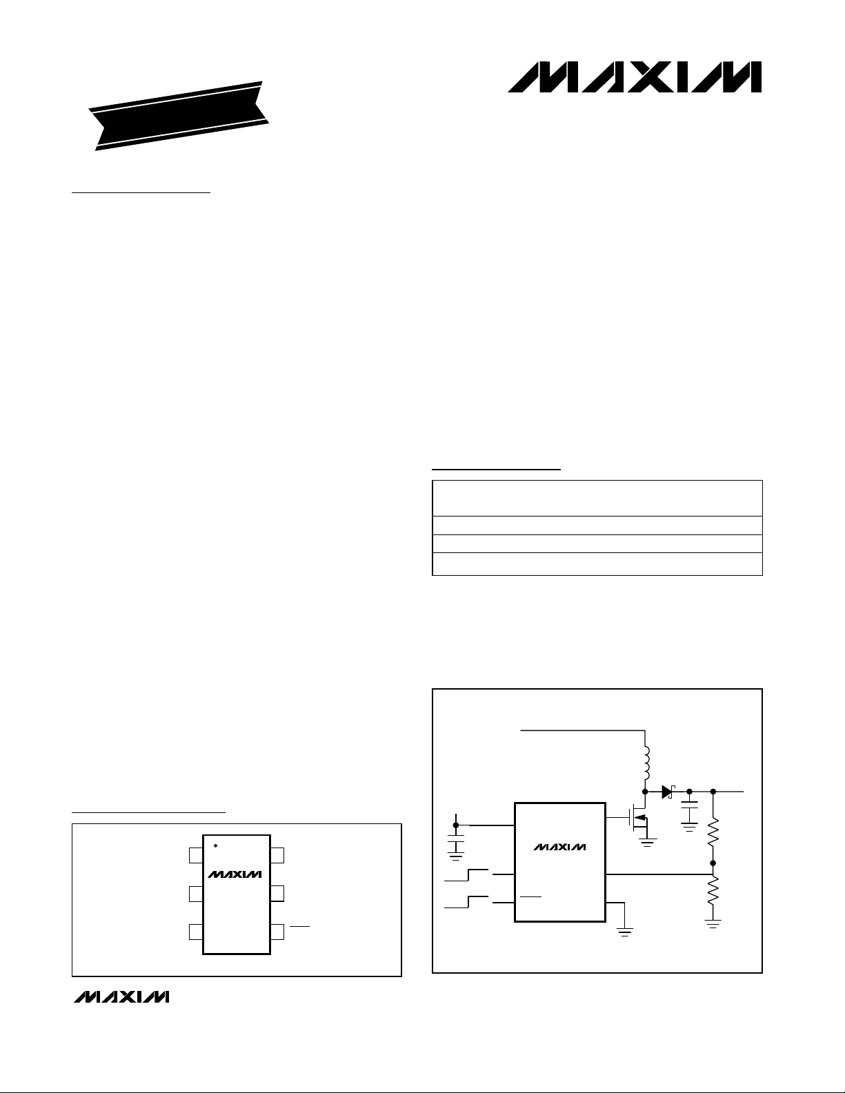
Pin Configurations
FB
SHDNSET
16V
CC
5 EXT
GND
MAX1522
MAX1523
MAX1524
SOT23-6
TOP VIEW
2
34
Low-Cost, High-Current,
or High-Voltage Boost
Conversion
LCD Bias Supplies
Industrial +24V and +28V
Power Supplies
Low-Cost, Multi-Output
Flyback Converters
SEPIC Converters
Low-Cost Battery-
Powered Applications
-40°C to +85°C
-40°C to +85°C
-40°C to +85°C
INPUT
OUTPUT
V
CC
6
V
CC
EXT
5
N
MAX1522
3
MAX1523
4
SET
SHDN
MAX1524
50% 85%
OFF ON
GND
2
FB
1
Page 2
Simple SOT23 Boost Controllers
2 _______________________________________________________________________________________
ABSOLUTE MAXIMUM RATINGS
ELECTRICAL CHARACTERISTICS
(VCC= SHDN = 3.3V, SET = GND , TA= -40°C to +85°C, unless otherwise noted. Typical values are at TA= +25°C.)
Stresses beyond those listed under “Absolute Maximum Ratings” may cause permanent damage to the device. These are stress ratings only, and functional
operation of the device at these or any other conditions beyond those indicated in the operational sections of the specifications is not implied. Exposure to
absolute maximum rating conditions for extended periods may affect device reliability.
Note 1: Actual startup voltage is dependent on the external MOSFET’s V
GS(TH)
.
Note 2: Specification applies after soft-start mode is completed.
V
CC
, FB, SHDN, SET to GND...................................-0.3V to +6V
EXT to GND................................................-0.3V to (V
CC
+ 0.3V)
Continuous Power Dissipation (TA= +70°C)
6-Pin SOT23 (derate 8.7mW/°C above +70°C) ..........696mW
Operating Temperature Range ..........................-40°C to +85°C
Junction Temperature......................................................+150°C
Storage Temperature Range.............................-65°C to +150°C
Lead Temperature (soldering, 10s) ................................+300°C
PARAMETER CONDITIONS
MIN
TYP
MAX
UNITS
VCC Operating Voltage Range 2.5 5.5 V
MAX1522/MAX1523 2.5
V
CC
Minimum Startup Voltage
f
EXT
> 100kHz, MAX1524 (Note 1), bootstrap required 1.5
V
VCC rising
Undervoltage Lockout
Threshold
V
CC
falling
V
V
CC
Supply Current No load, nonbootstrapped 25 50 µA
V
CC
Shutdown Current SHDN = GND
1µA
SET = GND 0.4 0.5 0.6
Fixed tON Time VFB =1.2V
SET = V
CC
2.4 3.0 3.6
µs
VFB > 0.675V 0.5
Minimum t
OFF
Time
V
FB
< 0.525V 1.0
µs
SET = GND 45 50 55
Maximum Duty Factor
SET = V
CC
80 85 90
%
FB Regulation Threshold
(Note 2)
V
CC
= +2.5V to +5.5V
V
FB Undervoltage Fault
Threshold (Note 2)
FB falling
575 625 mV
FB Input Bias Current VFB = 1.3V 6 50 nA
EXT high 2 4
EXT Resistance I
EXT
= 20mA
EXT low 1.5 3
Ω
Soft-Start Ramp Time 2.2 3.2 4.2 ms
Logic Input High VCC = +2.5V to +5.5V, SET, SHDN 1.6 V
Logic Input Low VCC = +2.5V to +5.5V, SET, SHDN 0.4 V
Logic Input Leakage Current SET, SHDN = VCC or GND -1 +1 µA
MAX1522/MAX1523/MAX1524
2.37 2.47
2.20 2.30
0.001
1.23 1.25 1.27
525
Page 3
MAX1522/MAX1523/MAX1524
Simple SOT23 Boost Controllers
_______________________________________________________________________________________ 3
100
50
0.1 1 100 1000
EFFICIENCY vs. LOAD CURRENT
(DESIGN EXAMPLE 1)
70
80
90
MAX1522/3/4 toc01
LOAD CURRENT (mA)
EFFICIENCY (%)
10
60
V
OUT
= +5V
V
IN
= 3.3V
100
50
0.1 1 100 1000
EFFICIENCY vs. LOAD CURRENT
(DESIGN EXAMPLE 2)
70
80
90
MAX1522/3/4 toc02
LOAD CURRENT (mA)
EFFICIENCY (%)
10
60
VIN = +4.2V
VIN = +3.6V
VIN = +2.7V
V
OUT
= +12V
100
50
0.1 1 100 1000
EFFICIENCY vs. LOAD CURRENT
(DESIGN EXAMPLE 3)
70
80
90
MAX1522/3/4 toc03
LOAD CURRENT (mA)
EFFICIENCY (%)
10
60
VIN = +2.4V
VIN = +1.8V
VIN = +3V
MAX1524
V
OUT
= +5V
100
50
0.1 1 100
EFFICIENCY vs. LOAD CURRENT
(DESIGN EXAMPLE 4)
70
80
90
MAX1522/3/4 toc04
LOAD CURRENT (mA)
EFFICIENCY (%)
10
60
VIN = +4.2V
VIN = +2.7V
VIN = +3.6V
V
OUT
= +24V
100
50
0.1 1 100
EFFICIENCY vs. LOAD CURRENT
(DESIGN EXAMPLE 5)
70
80
90
MAX1522/3/4 toc05
LOAD CURRENT (mA)
EFFICIENCY (%)
10
60
VIN = +3.0V
VIN = +2.4V
VIN = +1.8V
MAX1524
V
OUT
= +3.3V
1.75
1.50
1.25
1.00
0.75
05025 75 100
STARTUP INPUT VOLTAGE
vs. OUTPUT CURRENT
MAX1522/3/4 toc06
LOAD CURRENT (mA)
STARTUP VOLTAGE (V)
V
OUT
= +3.3V
BOOTSTRAPPED
RESISTIVE LOADS
10
0.0001
01 3 4
NO-LOAD INPUT CURRENT
vs. INPUT VOLTAGE
0.01
0.1
1
MAX1522/3/4 toc07
INPUT VOLTAGE (V)
INPUT CURRENT (mA)
2
0.001
NONBOOTSTRAPPED
BOOTSTRAPPED
5
400ns/div
SWITCHING WAVEFORM
(CONTINUOUS CONDUCTION)
VIN = +3.3V, V
OUT
= +5V, I
OUT
= 350mA
A : V
OUT
, 200mV/div, AC-COUPLED
B : V
LX
, 5V/div
C : I
L
, 0.5A/div
A
C
B
MAX1522/3/4 toc08
4µs/div
SWITCHING WAVEFORM
(DISCONTINUOUS CONDUCTION)
VIN = +3.3V, V
OUT
= +24V, I
OUT
= 10mA
A : V
OUT
, 200mV/div, AC-COUPLED
B : V
LX
, 10V/div
C : I
L
, 0.5A/div
A
C
B
MAX1522/3/4 toc09
Typical Operating Characteristics
(TA= +25°C, unless otherwise noted.)
Page 4
MAX1522/MAX1523/MAX1524
Simple SOT23 Boost Controllers
4 _______________________________________________________________________________________
Typical Operating Characteristics (continued)
(TA= +25°C, unless otherwise noted.)
400µs/div
SOFT-START RESPONSE
200Ω RESISTIVE LOAD
A : V
OUT
, 5V/div
B : V
SHDN
, 5V/div
C : I
L
, 1A/div
A
C
B
MAX1522/3/4 toc10
400µs/div
FAULT-DETECTION RESPONSE
A : V
OUT
, 10V/div
B : V
EXT
, 5V/div
C : I
L
, 5A/div
A
C
B
MAX1522/3/4 toc11
MAX1522
40µs/div
LINE-TRANSIENT RESPONSE
VIN = +3.5V TO +4.0V, V
OUT
= +12V, I
OUT
= 60mA
A : V
IN,
500mV/div, AC-COUPLED
B : V
OUT,
10mV/div, AC-COUPLED
A
B
MAX1522/3/4 toc12
100µs/div
LOAD-TRANSIENT RESPONSE
VIN = +3.3V, V
OUT
= +12V, I
OUT
= 30mA TO 120mA
A : I
OUT,
100mA/div
B : V
OUT,
100mV/div, AC-COUPLED
A
B
MAX1522/3/4 toc13
Page 5
Detailed Description
The MAX1522/MAX1523/MAX1524 are simple, compact boost controllers designed for a wide range of
DC-DC conversion topologies including step-up,
SEPIC, and flyback applications. These devices are
designed specifically to provide a simple application
circuit with a minimum of external components and are
ideal for PDAs, digital cameras, and other low-cost
consumer electronics applications.
These devices use a unique fixed on-time, minimum
off-time architecture, which provides excellent efficiency over a wide range of input/output voltage combinations and load currents. The fixed on-time is pin
selectable to either 0.5µs or 3µs, permitting optimization of external component size and ease of design for
a wide range of output voltages.
Control Scheme
The MAX1522/MAX1523/MAX1524 feature a unique
fixed on-time, minimum off-time architecture, which provides excellent efficiency over a wide range of
input/output voltage combinations. The fixed on-time is
pin selectable to either 0.5µs or 3µs for a maximum
duty factor of either 45% or 80%, respectively. An
inductor charging cycle is initiated by driving EXT high,
turning on the external MOSFET. The MOSFET remains
on for the fixed on-time, after which EXT turns off the
MOSFET. EXT stays low for at least the minimum off-
time, and another cycle begins when FB drops below
its 1.25V regulation point.
Bootstrapped vs. Nonbootstrapped
The VCCsupply voltage range of the MAX1522/
MAX1523/MAX1524 is +2.5V to +5.5V. The supply for
V
CC
can come from the input voltage (nonbootstrapped), the output voltage (bootstrapped), or an
independent regulator.
The MAX1522/MAX1523 are usually utilized in a nonbootstrapped configuration, allowing for high or low
output voltage operation. However, when both the input
and output voltages fall within the +2.5V to +5.5V
range, the MAX1522/MAX1523 may be operated in
nonbootstrapped or bootstrapped mode. Bootstrapped
mode provides higher gate-drive voltage to the MOSFET switch, reducing I2R losses in the switch, but will
also increase the VCCsupply current to charge and
discharge the gate. Depending upon the MOSFET
selected, there may be minor variation in efficiency vs.
load vs. input voltage when comparing bootstrapped
and nonbootstrapped configurations.
The MAX1524 is always utilized in bootstrapped configuration for applications where the input voltage range
extends down below 2.5V and the output voltage is
between 2.5V and 5.5V. VCCis connected to the output
(through a 10Ω series resistor) and receives startup
voltage through the DC current path from the input
through the inductor, diode, and 10Ω resistor. The
MAX1524 features a low-voltage startup oscillator that
MAX1522/MAX1523/MAX1524
Simple SOT23 Boost Controllers
_______________________________________________________________________________________ 5
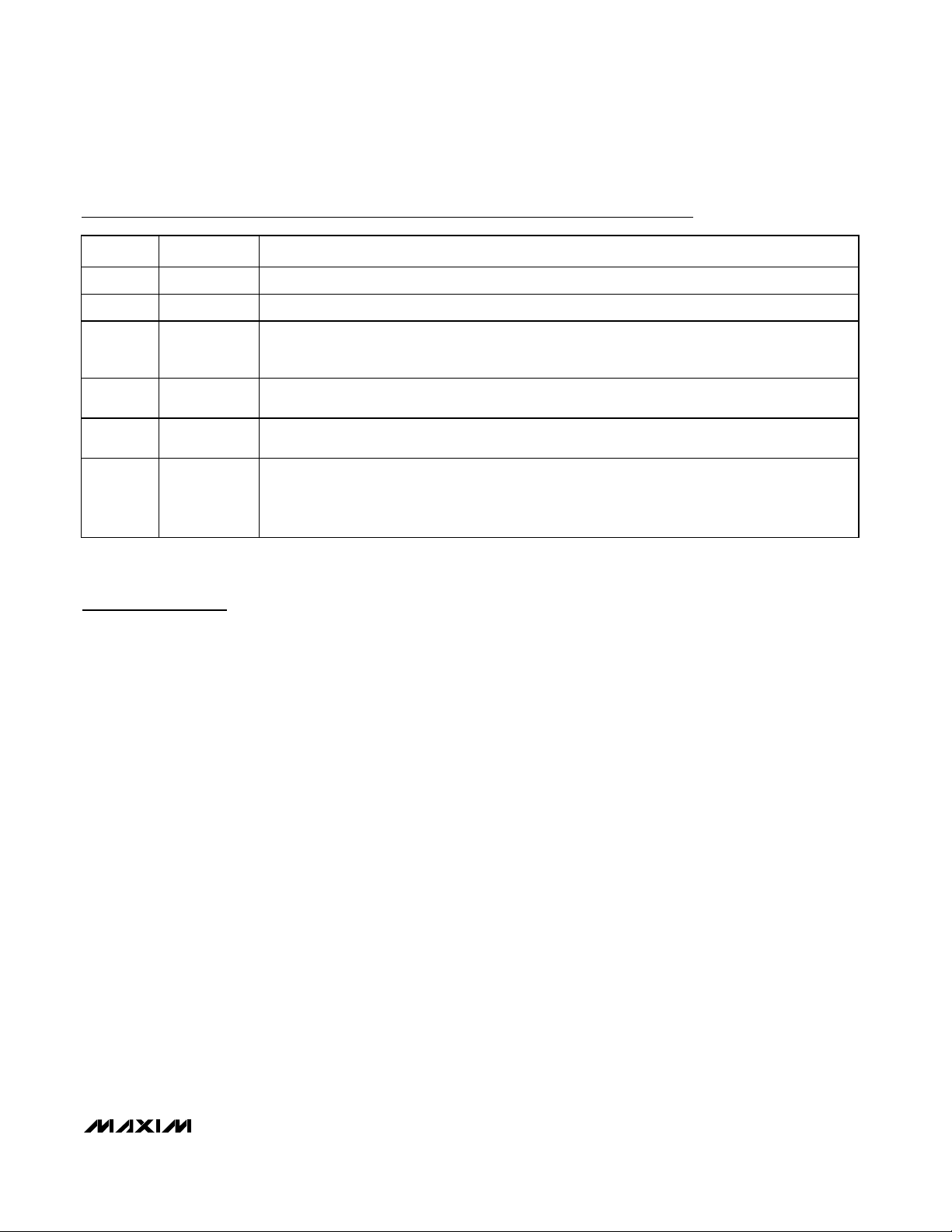
Pin Description
PIN NAME FUNCTION
1 GND Ground
2 FB Feedback Input. Connect FB to external resistive voltage-divider. FB regulates to 1.25V.
3 SET
On-Time Control. Connect SET to V
CC
to set the fixed 3µs on-time (85% duty cycle). Connect SET to
GND to set the fixed 0.5µs on-time (50% duty cycle). See On-Time SET Input section for more
information.
4 SHDN
Shutdown Control Input. Drive SHDN high for normal operation. Drive SHDN low for low-power
shutdown mode. Driving SHDN low clears the fault latch of the MAX1522 and MAX1524.
5 EXT
External MOSFET Drive. EXT drives the gate of an external NMOS power FET and swings from V
CC
to GND.
6V
CC
Supply Voltage to the IC. Bypass VCC to GND with a 0.1µF capacitor. Connect VCC to a +2.5V to
+5.5V supply, which may come from V
IN
(nonbootstrapped) or V
OUT
(bootstrapped) or from the
output of another regulator. For bootstrapped operation, connect V
CC
to the output through a series
10Ω resistor.
Page 6

MAX1522/MAX1523/MAX1524
Simple SOT23 Boost Controllers
6 _______________________________________________________________________________________
guarantees startup with input voltages down to 1.5V at
VCC. The startup oscillator has a fixed 25% duty cycle
and will toggle the MOSFET gate and begin boosting
the output voltage. Once the output voltage exceeds
the UVLO threshold, the normal control circuitry is used
and the startup oscillator is disabled. However, N-channel MOSFETs are rarely specified for guaranteed
R
DS(ON)
with VGSbelow 2.5V; therefore, guaranteed
startup down to 1.5V input will be limited by the MOSFET specifications. Nevertheless, the MAX1524 bootstrapped circuit on the MAX1524 EV kit typically starts
up with input voltage below 1V and no load.
The MAX1522/MAX1523 may also be utilized by connecting VCCto the output of an independent voltage
regulator between 2.5V and 5.5V to allow operation with
any combination of low or high input and output voltages. In this case, the independent regulator must supply enough current to satisfy the I
GATE
current as
calculated in the
Power MOSFET Selection section
when considering the maximum switching frequency as
calculated in the CCM or DCM design procedure.
On-Time SET Input
The MAX1522/MAX1523/MAX1524 feature pin-selectable fixed on-time control, allowing their operation to
be optimized for various input/output voltage combinations. Connect SET to V
CC
for the 3µs fixed on-time.
Connect SET to GND for the 0.5µs fixed on-time.
The 3µs on-time setting (SET = V
CC
) permits higher
than 80% guaranteed maximum duty factor, providing
improved efficiency in applications with higher step-up
ratios (such as 3.3V boosting to 12V). This setting is
recommended for higher step-up ratio applications.
The 0.5µs on-time setting (SET = GND) permits higher
frequency operation, minimizing the size of the external
inductor and capacitors. The maximum duty factor is
limited to 45% guaranteed, making this setting suitable
for lower step-up ratios such as 3.3V to 5V converters.
Soft-Start
The MAX1522/MAX1523/MAX1524 have a unique softstart mode that reduces inductor current during startup,
reducing battery, input capacitor, MOSFET, and inductor stresses. The soft-start period is fixed at 3.2ms and
requires no external components.
Fault Detection
Once the soft-start period has expired, if the output
voltage falls to, or is less than, 50% of its regulation
value, a fault is detected. Under this condition, the
MAX1522 disables the regulator until either SHDN is
toggled low or power is removed and reapplied, after
which it attempts to power up again in soft-start. For the
MAX1523, the fault condition is not latched, and softstart is repetitively reinitiated until a valid output voltage
is realized. The MAX1524 has a latched fault detection,
but when bootstrapped, the latch will be cleared when
V
CC
falls below 2.37V.
Shutdown Mode
Drive SHDN to GND to place the MAX1522/MAX1523/
MAX1524 in shutdown mode. In shutdown, the internal
reference and control circuitry turn off, EXT is driven to
GND, the supply current is reduced to less than 1µA,
and the output drops to one diode drop below the input
voltage. Connect SHDN to VCCfor normal operation.
When exiting shutdown mode, the 3.2ms soft-start is
always initiated.
Undervoltage Lockout
The MAX1522/MAX1523 have undervoltage lockout
(UVLO) circuitry, which prevents circuit operation and
MOSFET switching when VCCis less than the UVLO
threshold (2.37V typ). The UVLO comparator has 70mV
of hysteresis to eliminate chatter due to VCCinput
impedance.
Applications Information
Setting the Output Voltage
The output voltage is set by connecting FB to a resistive voltage-divider between the output and GND
(Figures 1 and 2). Select feedback resistor R2 in the
30kΩ to 100kΩ range. R1 is then given by:
where VFB= 1.25V.
Design Procedure
Continuous vs. Discontinuous Conduction
A switching regulator is operating in continuous conduction mode (CCM) when the inductor current is not
allowed to decay to zero. This is accomplished by
selecting an inductor value large enough that the
inductor ripple current becomes less than one half of
the input current. The advantage of this mode is that
peak current is lower, reducing I2R losses and output
ripple.
In general, the best transient performance and most of
the ripple reduction and efficiency increase of CCM are
realized when the inductance is large enough to
reduce the ripple current to 30% of the input current at
maximum load. It is important to note that CCM circuits
operate in discontinuous conduction mode (DCM)
RR
V
V
OUT
FB
12 1=−
Page 7

MAX1522/MAX1523/MAX1524
Simple SOT23 Boost Controllers
_______________________________________________________________________________________ 7
under light loads. The selection of 30% ripple current
causes this to happen at loads less than approximately
1/6th of maximum load.
There are two common reasons not to run in CCM:
1) High output voltage. In this case, the output-to-
input voltage ratio exceeds the level obtainable
by the MAX1522/MAX1523/MAX1524s’ maximum duty
factor. Calculate the application’s maximum duty cycle
using the equation in the Calculate the Maximum Duty
Cycle section. If this number exceeds 80%, you will
have to design for DCM.
2) Small output current. If the maximum output current
is very small, the inductor required for CCM may be
disproportionally large and expensive. Since I2R losses
are not a concern, it may make sense to use a smaller
inductor and run in DCM. This typically occurs when
the load current times the output-to-input voltage ratio
drops below a few hundred milliamps, although this
also depends on the external components.
Calculate the Maximum Duty Cycle
The maximum duty cycle of the application is given by:
where VDis the forward voltage drop of the Schottky
diode (about 0.5V).
Design Procedure for CCM
On-Time Selection
For CCM to occur, the MAX1522/MAX1523/MAX1524
must be able to exceed the application’s maximum
duty cycle. For applications up to 45% duty cycle, con-
nect SET to GND for 0.5µs on-time to get fast switching
and a smaller inductor. For applications up to 80% duty
cycle, it is necessary to connect SET to VCCfor 3.0µs
on-time. For applications greater than 80% duty cycle,
CCM operation is not guaranteed; see the Design
Procedure for DCM section.
Switching Frequency
A benefit of CCM is that the switching frequency
remains high as the load is reduced, whereas in DCM
the switching frequency varies directly with load. This is
important in applications where switching noise needs
to stay above the audio band. The medium- and heavyload switching frequency in CCM circuits is given by:
Note that f
SWITCHING
is not a function of load and
varies primarily with input voltage. However, when the
load is reduced, a CCM circuit drops into DCM, and
the frequency becomes load dependent:
Calculate the Peak Inductor Current
For CCM, the peak inductor current is given by:
I
VV
V
I
PEAK
OUT D
IN MIN
LOAD MAX
=×
+
×115.
()
()
ƒ≈×
+−
+
×
×
−SWITCHING LIGHT LOAD
ON
OUT D IN
OUT D
LOAD
LOAD MAX
t
VVV
VV
I
I
()
()
.1018
ƒ=×
+−
+
SWITCHING
ON
OUT D IN
OUT D
t
VVV
VV
1
DutyCycle
VVV
VV
MAX
OUT D INMIN
OUT D
()
=
+−
+
×
()
%100
MAX1522
MAX1523
INPUT
2.7V TO 4.2V
C3
0.1µF
OFF ON
6
3
4
5
2
1
V
CC
EXT
SET FB
SHDN GND
C1
10µF
6.3V
L1
33µH
CDR74B-330
D1
MBR0530T3
Q1
FDC633N
R1
130kΩ
1%
OUTPUT
12V
C2
33µF
TPSD336M020R0200
C
FB
220pF
C
FF
220pF
R1
15.0kΩ
1%
Figure 1. MAX1522/MAX1523 Standard Operating Circuit
Page 8

MAX1522/MAX1523/MAX1524
Simple SOT23 Boost Controllers
8 _______________________________________________________________________________________
Inductor Selection
For CCM, the ideal inductor value is given by:
If L
IDEAL
is not a standard value, choose the next-closest value, either higher or lower. Nominal values within
50% are acceptable. Values lower than ideal will have
slightly higher peak inductor current; values greater
than ideal will have slightly lower peak inductor current.
Due to the MAX1522/MAX1523/MAX1524s’ high switching frequencies, inductors with a ferrite core or equivalent are recommended. Powdered iron cores are not
recommended due to their high losses at frequencies
over 50kHz.
The saturation rating of the selected inductor should
meet or exceed the calculated value for I
PEAK
,
although most coil types can be operated up to 20%
over their saturation rating without difficulty. In addition
to the saturation criteria, the inductor should have as
low a series resistance as possible. The power loss in
the inductor resistance is approximately given by:
Output Capacitor Selection
In CCM, to provide stable operation and to control output sag to less than 0.5%, the output bulk capacitance
should be greater than:
To properly control peak inductor current during the
3.2ms soft-start, the output bulk capacitance should be
less than:
where t
SS
= 3.2ms.
Because the MAX1522/MAX1523/MAX1524 are voltage-mode devices (and therefore do not require an
expensive current-sense resistor), cycle-to-cycle stability is obtained from the output capacitor’s equivalent
series resistance (ESR). Choose an output capacitor
with actual ESR greater than:
Additionally, to control peak inductor current during softstart, the output capacitor’s ESR should be greater
than:
Usually, this prevents the use of ceramic capacitors in
CCM applications. Alternatives include tantalum, electrolytic, and organic types such as Sanyo’s POSCAP.
The output capacitor must also be rated to withstand
the output voltage and the output ripple current, which
is equivalent to I
PEAK
. Since output ripple in boost DC-
DC designs is dominated by capacitor ESR, a capaci-
ESR
V
I
COUT
FB
PEAK
>× ×
−
60 10
3
ESR
L
C
I
V
COUT
OUT
LOAD MAX
IN MIN
>×
()
()
C
It
V
OUT MAX
LOAD MAX SS
OUT
()
()
=
×
C
It
V
OUT MIN
LOAD MAX ON
OUT
()
()
.
=
×
×0 005
P
IVV
V
LR
LOAD OUT D
IN
R
L
≅
×+
×
()
2
L
Vt
I
IDEAL
IN TYP ON TYP
PEAK
=
×
×
() ()
.03
MAX1524
INPUT
3.3V ±10%
C3
0.1µF
OFF ON
6
3
4
5
2
1
V
CC
EXT
SET FB
SHDN GND
C1
10µF
6.3V
L1
33µH
CR43-3R3
D1
CRS01
Q1
FDC633N
R1
100kΩ
1%
OUTPUT
5V
C2
33µF
10TPA33M
C
FF
100pF
R2
33.2kΩ
1%
R3
10Ω
Figure 2. MAX1524 Standard Operating Circuit
Page 9

MAX1522/MAX1523/MAX1524
Simple SOT23 Boost Controllers
_______________________________________________________________________________________ 9
tance value two or three times larger than C
OUT(MIN)
is
typically needed. Output ripple due to ESR is:
at light and medium loads, and three times as great at
peak load.
Continue the CCM design procedure by going to the
Optional Feed-Forward Capacitor Selection section.
Design Procedure for DCM
On-Time Selection
The MAX1522/MAX1523/MAX1524 may operate in
DCM at any duty cycle as required by the application’s
input and output voltages. However, best performance
is achieved when the maximum duty cycle of the application is similar to the MAX1522/MAX1523/MAX1524s’
maximum duty factor as set using the SET input.
Connect SET to GND for applications with maximum
duty cycles less than 67%. Connect SET to V
CC
for
applications with maximum duty cycles between 67%
and 99%.
Inductor Selection
For DCM, the ideal inductor value is given by:
If L
IDEAL
is not a standard value, choose the next lower
nominal value. The above formula already includes a
factor for ±30% inductor tolerance. Values higher than
ideal may not supply the maximum load when the input
voltage is low, while values much lower than ideal will
have poorer efficiency.
Calculate the Peak Inductor Current
For DCM, the peak inductor current is given by:
The saturation rating of the selected inductor should
meet or exceed the calculated value for I
PEAK
,
although most coil types can be operated up to 20%
over their saturation rating without difficulty. In addition
to the saturation criteria, the inductor should have as
low a series resistance as possible. The power loss in
the inductor resistance is approximately given by:
Due to the MAX1522/MAX1523/MAX1524s’ high switching frequencies, inductors with a ferrite core or equivalent are recommended. Powdered iron cores are not
recommended due to their high losses at frequencies
over 50kHz.
Switching Frequency
In DCM, the switching frequency is proportional to the
load current and is approximately given by:
Note that f
SWITCHING
is a function of load and input
voltage.
Output Capacitor Selection
In DCM, the MAX1522/MAX1523/MAX1524 may use
either a ceramic output capacitor (with very low ESR) or
other capacitors, such as tantalum or organic, with
higher ESR. For less than 2% output ripple, the minimum value for ceramic output capacitors should be
greater than:
To control inductor current during soft-start, the maximum value for any type of output capacitors should be
less than:
where tSS= 3.2ms.
The capacitor should be chosen to provide an output
ripple between 25mV minimum and 2% of V
OUT
maximum. The output ripple due to capacitance ripple and
ESR ripple can be approximated by:
For output ripple close to 2% of V
OUT
, the optional
feed-forward capacitor may not be required. For lower
output ripple, a feed-forward capacitor is necessary for
stability and to control inductor current during soft-start.
V
L
tV
VVVC
t
L
ESR
RIPPLE COUT ESR
ON IN
OUT D IN OUT
ON
COUT
()+
≅×
×
+−
()
×
×
×
1
2
1
22
+
V
IN
C
It
V
OUT MAX
LOAD MAX SS
OUT
()
()
=
×
C
L
tV
VVV V
OUT MIN
ON IN
OUT D IN OUT
()
.
=×
×
+−
()
×
1
2
1
002
22
ƒ≈×
+−
()
×
×
SWITCHING OUT
OUT D IN
ON IN
I
VVV
tV
L07 2
22
.
PII
VV
V
LR PEAK OUT
OUT D
IN
R
L
≅××
+
2
3
I
Vt
L
PEAK
IN MAX ON MAX
=
×
() ()
L
Vt
VVI
IDEAL
IN MIN ON MIN
OUT D LOAD MAX
=
×
×+×
()
()
() ()
()
2
3
V I ESR
RIPPLE ESR PEAK COUT()
.≅× ×03
Page 10

MAX1522/MAX1523/MAX1524
Simple SOT23 Boost Controllers
10 ______________________________________________________________________________________
Optional Feed-Forward
Capacitor Selection
For proper control of peak inductor current during softstart and for stable switching, the ripple at FB should
be greater than 25mV. Without a feed-forward capacitor connected between the output and FB, the output’s
ripple must be at least 2% of V
OUT
in order to meet this
requirement. Alternatively, if a low-ESR output capacitor
is chosen to obtain small output ripple, then a feed-forward capacitor should be used, and the output ripple
may be as low as 25mV. The approximate value of the
feed-forward capacitor is given by:
Do not use a feed-forward capacitor that is much larger
than this because line-transient performance will
degrade. Do not use a feed-forward capacitor at all if
the output ripple is large enough without it to provide
stable switching because load regulation will degrade.
Optional Feedback Capacitor Selection
When using a feed-forward capacitor, it is possible to
achieve too much ripple at FB. The symptoms of this
include excessive line and load regulation and possibly
high output ripple at light loads in the form of pulse
groupings or “bursts.” Fortunately, this is easy to correct by either choosing a lower-ESR output capacitor or
by adding a feedback capacitor between FB and
ground. This feedback capacitor (CFB), along with the
feed-forward capacitor, form an AC-coupled ripple voltage-divider from the output to FB:
It is relatively simple to determine a good value for C
FB
experimentally. Start with CFB= CFFto cut the FB ripple
in half; then increase or decrease CFBas needed. The
ideal ripple at FB is from 25mV to 40mV, which will provide stable switching, low output ripple at light and
medium loads, and reasonable line and load regulation. Never use a feedback capacitor without also using
a feed-forward capacitor.
Input Capacitor Selection
The input capacitor (CIN) in boost designs reduces the
current peaks drawn from the input supply, increases
efficiency, and reduces noise injection. The source
impedance of the input supply largely determines the
value of CIN. High source impedance requires high
input capacitance, particularly as the input voltage
falls. Since step-up DC-DC converters act as “constantpower” loads to their input supply, input current rises
as input voltage falls. Consequently, in low-input-voltage designs, increasing CINand/or lowering its ESR
can add as many as five percentage points to conversion efficiency. A good starting point is to use the same
capacitance value for CINas for C
OUT
. The input
capacitor must also meet the ripple current requirement
imposed by the switching currents, which is about 30%
of I
PEAK
in CCM designs and 100% of I
PEAK
in DCM
designs.
In addition to the bulk input capacitor, a ceramic 0.1µF
bypass capacitor at VCCis recommended. This capacitor should be located as close to VCCand GND as possible. In bootstrapped configuration, it is recommended
to isolate the bypass capacitor from the output capacitor with a series 10Ω resistor between the output and
V
CC
.
Power MOSFET Selection
The MAX1522/MAX1523/MAX1524 drive a wide variety
of N-channel power MOSFETs (NFETs). Since the output gate drive is limited to VCC, a logic-level NFET is
required. Best performance, especially when VCCis
less than 4.5V, is achieved with low-threshold NFETs
that specify on-resistance with a gate-source voltage
(V
GS
) of 2.7V or less. When selecting an NFET, key
parameters include:
1) Total gate charge (Qg)
2) Reverse transfer capacitance or charge (C
RSS
)
3) On-resistance (R
DS(ON)
)
4) Maximum drain-to-source voltage (V
DS(MAX)
)
5) Minimum threshold voltage (V
TH(MIN)
)
At high switching rates, dynamic characteristics (parameters 1 and 2 above) that predict switching losses
may have more impact on efficiency than R
DS(ON)
,
which predicts I2R losses. Qg includes all capacitances
associated with charging the gate. In addition, this
parameter helps predict the current needed to drive the
gate when switching at high frequency. The continuous
VCCcurrent due to gate drive is:
Use the FET manufacturer’s typical value for Qg (see
manufacturer’s graph of Qg vs. Vgs) in the above
equation since a maximum value (if supplied) is usually
too conservative to be of any use in estimating I
GATE
.
IQg
GATE SWITCHING
=׃
Ripple Ripple
C
CC
FB OUTPUT
FF
FB FF
=
+
×
C
RR
FF
≅× +
−
310
111
2
6
Page 11

MAX1522/MAX1523/MAX1524
Simple SOT23 Boost Controllers
______________________________________________________________________________________ 11
Diode Selection
The MAX1522/MAX1523/MAX1524s’ high switching fre-
quency demands a high-speed rectifier. Schottky
diodes are recommended for most applications
because of their fast recovery time and low forward
voltage. Ensure that the diode’s current rating is adequate to withstand the diode’s RMS current:
Also, the diode reverse breakdown voltage must
exceed V
OUT
. For high output voltages (50V or above),
Schottky diodes may not be practical because of this
voltage requirement. In these cases, use a high-speed
silicon rectifier with adequate reverse voltage. Another
consideration for high input voltages is reverse leakage
of the diode. This should be considered using the manufacturer’s specification due to its direct influence on
system efficiency.
Layout Considerations
High switching frequencies and large peak currents
make PC board layout a very important part of design.
Good design minimizes excessive EMI on the feedback
paths and voltage gradients in the ground plane, both
of which can result in instability or regulation errors.
Connect the inductor, input filter capacitor, and output
filter capacitor as close together as possible, and keep
their traces short, direct, and wide. Connect their
ground pins at a single common node in a star-ground
configuration. The external voltage-feedback network
should be very close to the FB pin, within 0.2in (5mm).
Keep noisy traces (such as the trace from the junction
of the inductor and MOSFET) away from the voltagefeedback network; also keep them separate, using
grounded copper. The MAX1522/MAX1523/ MAX1524
evaluation kit manual shows an example PC board layout and routing scheme.
Generating Resistance
with PC Board Traces
If the output capacitor’s ESR is too low for proper regulation, it can be increased artificially directly on the PC
board. For example, an additional 50mΩ of ESR added
to the output capacitor provides best regulation. The
resistivity of a 10mil trace using 1oz copper is about
50mΩ per inch. Therefore, a 10mil trace 1in long generates the required resistance.
III
DIODE RMS OUT PEAK()
<×
Page 12

MAX1522/MAX1523/MAX1524
Simple SOT23 Boost Controllers
12 ______________________________________________________________________________________
PARAMETER EXAMPLE 1 EXAMPLE 2 EXAMPLE 3
V
IN
3.3V ±10% 2.7V to 4.2V 1.8V to 3.0V
V
OUT
5V 12V 5V
I
OUT(MAX)
700mA 200mA 1.0A
R1, R2
274kΩ, 90.9kΩ 866kΩ, 100kΩ 274kΩ, 90.9kΩ
Duty Cycle (max) 45.5% 78.4% 67.3%
t
ON
0.5µs (SET = GND) 3µs (SET = VCC) 3µs (SET = VCC)
f
SWITCHING
691kHz to 909kHz
when I
OUT
> 120mA
221kHz to 261kHz
when I
OUT
> 35mA
152kHz to 224kHz
when I
OUT
> 167mA
I
PEAK
1.48A 1.06A 3.51A
L
IDEAL
3.73µH 33.8µH 6.83µH
L
ACTUAL
Sumida CR43-3R3
3.3µH, 86mΩ, 1.44A
Sumida CDR74B-330
33µH, 180mΩ, 0.97A
Sumida CDRH125-5R8
5.8µH, 17mΩ, 4.4A
P
LR
29mW at I
OUT
= 350mA 22mW at I
OUT
= 100mA 22mW at I
OUT
= 500mA
C
OUT(MIN)
to C
OUT(MAX)
14µF to 448µF 10µF to 53µF 120µF to 640µF
C
OUT
33µF 33µF 150µF
ESR
COUT(MIN)
23mΩ for stability,
51mΩ for soft-start
74mΩ for stability,
70mΩ for soft-start
21mΩ for stability,
21mΩ for soft-start
C
OUT(ACTUAL)
Sanyo POSCAP 10TPA33M
33µF, 10V,
60mΩ, 100mΩ max
AVX TPSD336M020R0200
33µF, 20V,
150mΩ, 200mΩ max
Sanyo POSCAP 6TPB150M
150µF, 6.3V,
40mΩ, 55mΩ max
V
RIPPLE(ESR)
27mVp-p at light loads,
81mVp-p at full load
48mVp-p at light loads,
144mVp-p at full load
42mVp-p at light loads,
126mVp-p at full load
C
FF
100pF 100pF 100pF
C
FB
100pF 330pF 220pF
C
IN
10µF, 6.3V ceramic 10µF, 6.3V ceramic 10µF, 6.3V ceramic
MOSFET Fairchild FDC633N Fairchild FDC633N Vishay Si3446DV
Qg
8nC at Vgs = 3V
12nC at Vgs = 5V
9nC at Vgs = 3.6V 10nC at Vgs = 5V
I
GATE
7.3mA nonbootstrapped,
10.9mA bootstrapped
2.4mA nonbootstrapped 2.2mA bootstrapped
I
DIODE(RMS)
0.96A 0.49A 1.84A
Diode Nihon EP10QY03, 1A Nihon EP10QY03, 1A Nihon EC21QS03L, 2A
Table 1. Design Examples Using CCM
Page 13

MAX1522/MAX1523/MAX1524
Simple SOT23 Boost Controllers
______________________________________________________________________________________ 13
PARAMETER EXAMPLE 4 EXAMPLE 5
V
IN
2.7V to 4.2V 1.8V to 3.0V
V
OUT
24V 3.3V
I
OUT(MAX)
30mA 100mA
R1, R2 909kΩ, 49.9kΩ 150kΩ, 93.1kΩ
Duty Cycle (max) 89.0% 52.6%
t
ON
3µs
(SET = V
CC
)
0.5µs
(SET = GND)
L
IDEAL
11.9µH 1.14µH
L
ACTUAL
Sumida
CDRH5D28-100
10µH, 65mΩ,
1.3A
Sumida
CDRH4D18-1R0
1µH, 45mΩ,
1.72A
I
PEAK
1.51A 1.80A
P
LR
4.5mW at
I
OUT
= 10mA
5.7mW
I
OUT
= 50mA
f
SWITCHING
208kHz when
I
OUT
= 20mA
737kHz when
I
OUT
= 100mA
C
OUT(MIN)
to
C
OUT(MAX)
0.8µF to 2.7µF 3µF to 97µF
C
OUT(ACTUAL)
Taiyo Yuden
2.2µF, X5R, 35V,
1210
Taiyo Yuden
TMK316BT106ML
10µF, X7R, 6.3V,
1206
ESR
COUT(ACTUAL)
10mΩ 10mΩ
V
RIP P LE ( C OU T+ E S R )
126mVp-p 40mVp-p
C
FF
100pF 220pF
C
FB
220pF 100pF optional
C
IN
10µF, 6.3V 10µF, 6.3V
MOSFET
Fairchild
FDC633N
Vishay Si2302DS
Qg
5nC at Vgs = 3.3V
I
GATE
1.7mA
3.7mA
bootstrapped
I
DIODE(RMS)
0.17A 0.42A
Diode
Nihon
EP10QY03, 1A
Nihon
EP10QY03, 1A
Table 2. Design Examples Using DCM
MANUFACTURER
PHONE WEB
Coilcraft
www.coilcraft.com
Fairchild
www.fairchildsemi.com
International
Rectifier
www.irf.com
Kemet
www.kemet.com
NIC Components
www.niccomp.com
Panasonic
www.panasonic.com
Sumida
www.sumida.com
Taiyo Yuden
www.t-yuden.com
Table 3. Component Manufacturers
Chip Information
TRANSISTOR COUNT: 1302
GMK325BJ225K
8nC at Vgs = 3V
nonbootstrapped
847-639-6400
800-341-0392
310-322-3331
408-986-0424
408-954-8470
847-468-5624
847-956-0666
408-573-4150
Page 14

MAX1522/MAX1523/MAX1524
Simple SOT23 Boost Controllers
Package Information
6LSOT.EPS
Maxim cannot assume responsibility for use of any circuitry other than circuitry entirely embodied in a Maxim product. No circuit patent licenses are
implied. Maxim reserves the right to change the circuitry and specifications without notice at any time.
14 ____________________Maxim Integrated Products, 120 San Gabriel Drive, Sunnyvale, CA 94086 408-737-7600
© 2001 Maxim Integrated Products Printed USA is a registered trademark of Maxim Integrated Products.
 Loading...