

Page 1
General Description
The MAX1510 DDR linear regulator sources and sinks up
to 3A peak (typ) using internal n-channel MOSFETs. This
linear regulator delivers an accurate 0.5V to 1.5V output
from a low-voltage power input (V
IN
= 1.1V to 3.6V). The
MAX1510 uses a separate 3.3V bias supply to power the
control circuitry and drive the internal n-channel
MOSFETs.
The MAX1510 provides current and thermal limits to
prevent damage to the linear regulator. Additionally,
the MAX1510 generates a power-good (PGOOD) signal
to indicate that the output is in regulation. During startup, PGOOD remains low until the output is in regulation
for 2ms (typ). The internal soft-start limits the input
surge current.
The MAX1510 powers the active-DDR termination bus
that requires a tracking input reference. The MAX1510
can also be used in low-power chipsets and graphics
processor cores that require dynamically adjustable
output voltages. The MAX1510 is available in a 10-pin
3mm x 3mm thin DFN package.
Applications
Notebook/Desktop Computers
DDR Memory Termination
Active Termination Buses
Graphics Processor Core Supplies
Chipset/RAM Supplies as Low as 0.5V
Features
♦ Internal Power MOSFETs with Current Limit (3A typ)
♦ Fast Load-Transient Response
♦ External Reference Input with Reference
Output Buffer
♦ 1.1V to 3.6V Power Input
♦ ±15mV (max) Load-Regulation Error
♦ Thermal Fault Protection
♦ Shutdown Input
♦ Power-Good Window Comparator with 2ms
(typ) Delay
♦ Small, Low-Profile 10-Pin 3mm x 3mm TDFN
Package
♦ Ceramic or Polymer Output Capacitors
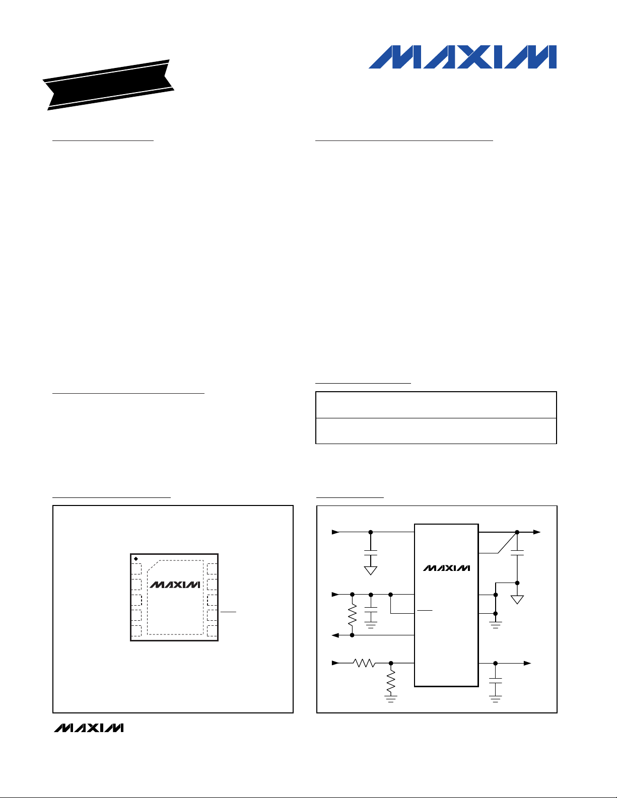
MAX1510
Low-Voltage DDR Linear Regulator
________________________________________________________________ Maxim Integrated Products 1
Ordering Information
OUT
IN
OUTS
AGND
PGND
V
OUT
= V
TT
V
IN
(1.1V TO 3.6V)
V
BIAS
(2.7V TO 3.6V)
V
DDQ
(2.5V OR 1.8V)
V
REFOUT
= V
TTR
REFOUT
MAX1510
V
CC
PGOOD
SHDN
REFIN
Typical Operating Circuit
19-3279; Rev 0; 5/04
For pricing, delivery, and ordering information, please contact Maxim/Dallas Direct! at
1-888-629-4642, or visit Maxim’s website at www.maxim-ic.com.
EVALUATION KIT
AVAILABLE
Pin Configuration
PART TEMP RANGE
MAX1510ETB -40°C to +85°C
PIN-
PACKAGE
10 TDFN
(3mm x 3mm)
TOP
MARK
ABD
TOP VIEW
1 INREFOUT
2
V
CC
AGND
REFIN
3
4
5
3mm x 3mm
MAX1510
TDFN
10
98OUT
7
6
PGND
SHDN
OUTSPGOOD
Page 2
MAX1510
Low-Voltage DDR Linear Regulator
2 _______________________________________________________________________________________
ABSOLUTE MAXIMUM RATINGS
ELECTRICAL CHARACTERISTICS
(VIN= 1.8V, VCC= 3.3V, V
REFIN
= V
OUTS
= 1.25V, SHDN = VCC, circuit of Figure 1, TA= -40°C to +85°C, unless otherwise noted.
Typical values are at T
A
= +25°C.) (Note 1)
Stresses beyond those listed under “Absolute Maximum Ratings” may cause permanent damage to the device. These are stress ratings only, and functional
operation of the device at these or any other conditions beyond those indicated in the operational sections of the specifications is not implied. Exposure to
absolute maximum rating conditions for extended periods may affect device reliability.
IN to PGND...............................................................-0.3V to +4V
OUT to PGND ..............................................-0.3V to (V
IN
+ 0.3V)
OUTS to AGND............................................-0.3V to (V
IN
+ 0.3V)
V
CC
to AGND............................................................-0.3V to +4V
REFIN, REFOUT, SHDN, PGOOD to AGND ..-0.3V to (V
CC
+ 0.3V)
PGND to AGND .....................................................-0.3V to +0.3V
REFOUT Short Circuit to AGND .................................Continuous
OUT Continuous RMS Current: 100s ..................................±1.6A
1s......................................±2.5A
Continuous Power Dissipation (T
A
= +70°C)
10-Pin 3mm x 3mm Thin DFN
(derated 24.4mW/°C above +70°C)...........................1951mW
Operating Temperature Range
MAX1510ETB...................................................-40°C to +85°C
Junction Temperature......................................................+150°C
Storage Temperature Range .............................-65°C to +150°C
Lead Temperature (soldering, 10s) .................................+300°C
)
)
PARAMETER SYMBOL CONDITIONS MIN TYP MAX UNITS
Input Voltage Range
Quiescent Supply Current (VCC)ICCLoad = 0, V
Shutdown Supply Current (VCC)I
Quiescent Supply Current (VIN)IINLoad = 0 0.4 10 mA
Shutdown Supply Current (VIN)I
Feedback-Voltage Error V
Load-Regulation Error -1A ≤ I
Line-Regulation Error 1.4V ≤ VIN ≤ 3.3V, I
OUTS Input Bias Current I
OUTPUT
Output Adjust Range 0.5 1.5 V
OUT On-Resistance
Output Current Slew Rate C
OUT Power-Supply Rejection
Ratio
OUT to OUTS Resistance R
Discharge MOSFET OnResistance
V
V
CC(SHDN
IN(SHDN
OUTS
OUTS
PSRR
OUTS
R
DISCHARGE
IN
CC
Power input 1.1 3.6
Bias supply 2.7 3.6
> 0.45V 0.7 1.3 mA
REFIN
SHDN = GND, V
> 0.45V 350 600 µA
REFIN
SHDN = GND, REFIN = GND 50 100 µA
SHDN = GND 0.1 10 µA
REFIN to OUTS
I
= ±200mA
OUT
≤ +1A -15 +15 mV
OUT
High-side MOSFET (source) (I
Low-side MOSFET (sink) (I
= 100µF, I
OUT
10Hz < f < 10kHz, I
= 100µF
C
OUT
TA = 25°C-40+4
T
= -40°C to +85°C-6 +6
A
= ±100mA 1 mV
OUT
= 0.1A) 0.10 0.25
OUT
= -0.1A) 0.10 0.25
OUT
= 0.1A to 2A 3 A/µs
OUT
= 200mA,
OUT
SHDN = GND 8 Ω
-1 +1 µA
80 dB
12 kΩ
V
mV
Ω
Page 3
MAX1510
Low-Voltage DDR Linear Regulator
_______________________________________________________________________________________ 3
Note 1: Limits are 100% production tested at TA= +25°C. Limits over the operating temperature range are guaranteed through cor-
relation using statistical-quality-control (SQC) methods.
ELECTRICAL CHARACTERISTICS (continued)
(VIN= 1.8V, VCC= 3.3V, V
REFIN
= V
OUTS
= 1.25V, SHDN = VCC, circuit of Figure 1, TA= -40°C to +85°C, unless otherwise noted.
Typical values are at T
A
= +25°C.) (Note 1)
REFERENCE
REFIN Voltage Range V
REFIN Input Bias Current I
REFIN Undervoltage-Lockout
Voltage
REFOUT Voltage V
REFOUT Load Regulation ∆V
FAULT DETECTION
Thermal-Shutdown Threshold T
VCC Undervoltage-Lockout
Threshold
IN Undervoltage-Lockout
Threshold
Current-Limit Threshold I
Soft-Start Current-Limit Time t
INPUTS AND OUTPUTS
PGOOD Lower Trip Threshold
PGOOD Upper Trip Threshold
PGOOD Propagation Delay t
PGOOD Startup Delay
PGOOD Output Low Voltage I
PGOOD Leakage Current I
SHDN Logic Input Threshold
SHDN Logic Input Current SHDN = VCC or GND -1 +1 µA
PARAMETER SYMBOL CONDITIONS MIN TYP MAX UNITS
REFIN
REFIN
REFOUTVCC
REFOUTIREFOUT
SHDN
V
UVLO
LIMIT
SS
PGOOD
PGOOD
0.5 1.5 V
-1 +1 µA
Rising edge, hysteresis = 75mV 0.35 0.45 V
V
= 3.3V, I
= ±5mA -20 +20 mV
Rising edge, hysteresis = 15°C +165 °C
Rising edge, hysteresis = 100mV 2.45 2.55 2.65 V
Rising edge, hysteresis = 55mV 0.9 1.1 V
With respect to feedback threshold,
hysteresis = 12mV
With respect to feedback threshold,
hysteresis = 12mV
OUTS forced 25mV beyond PGOOD trip
threshold
Startup rising edge, OUTS within ±100mV of
the feedback threshold
= 4mA 0.3 V
SINK
OUTS = REFIN (PGOOD high impedance),
PGOOD = V
Logic high 2.0 V
Logic low 0.8 V
CC
REFOUT
+ 0.3V
= 0
REFIN
-0.01
-200 -150 -100 mV
V
REFIN
1.8 3 4.2 A
100 150 200 mV
51035µs
1 2 3.5 ms
V
REFIN
+0.01
200 µs
1µA
V
Page 4
MAX1510
Low-Voltage DDR Linear Regulator
4 _______________________________________________________________________________________
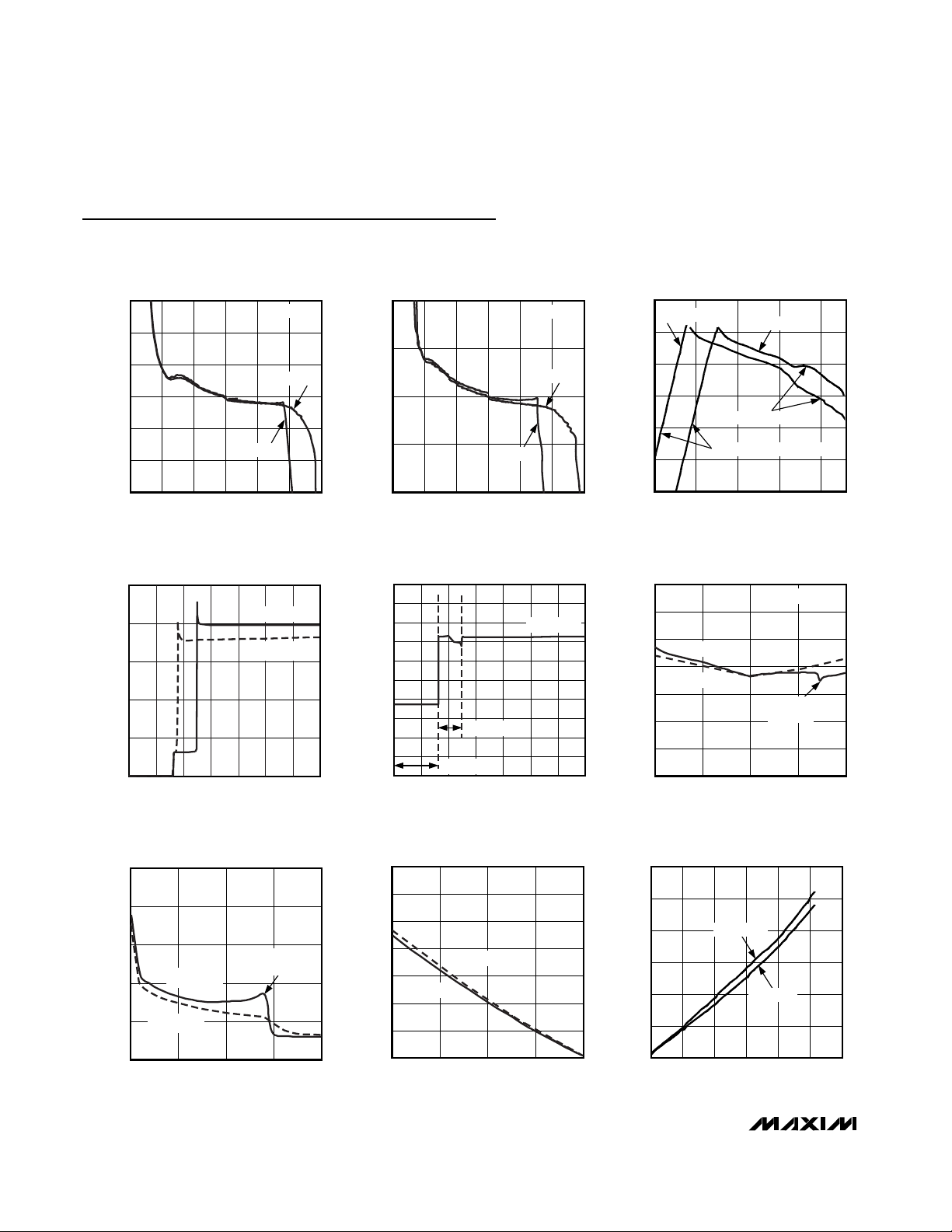
Typical Operating Characteristics
(Circuit of Figure 1. TA = +25°C, unless otherwise noted)
INPUT CURRENT (IIN)
vs. INPUT VOLTAGE (V
IN
)
MAX1510 toc04
VIN (V)
I
IN
(µA)
3.02.52.01.51.00.5
50
100
150
200
250
0
0.0 3.5
V
OUT
= 1.25V
V
OUT
= 0.90V
0.96
OUTPUT LOAD REGULATION
0.94
(V)
V
OUT
0.92
0.90
0.88
0.86
V
VIN = 1.2V
REFIN
VIN = 1.5V
= 0.9V
MAX1510 toc01
(V)
V
OUT
1.300
1.275
1.250
1.225
OUTPUT LOAD REGULATION
V
REFIN
VIN = 1.8V
VIN = 1.5V
= 1.25V
3.0
V
OUT
2.5
MAX1510 toc02
2.0
1.5
1.0
MAXIMUM OUTPUT CURRENT (A)
0.5
MAXIMUM OUTPUT CURRENT
vs. INPUT VOLTAGE
= 0.9V
V
= 1.25V
OUT
THERMALLY LIMITED
DROPOUT VOLTAGE LIMITED
MAX1510 toc03
0.84
-3 3-2 -1 0 1 2
I
(A)
OUT
1.200
-3 3-2 -1 0 1 2
I
(A)
OUT
BIAS CURRENT (ICC)
vs. INPUT VOLTAGE (V
1.0
0.9
0.8
0.7
0.6
(mA)
0.5
IN
I
0.4
0.3
0.2
0.1
0.0
0.0 3.5
POWER GROUND CURRENT (I
vs. SOURCE LOAD CURRENT (I
0.25
0.20
0.15
(mA)
PGND
I
0.10
0.05
0.00
V
= 1.25V
OUT
V
= 0.90V
OUT
0.0 2.0
I
OUT
(A)
PGND
OUT
VIN = 1.5V
ENTERING
DROPOUT
1.51.00.5
)
)
MAX1510 toc07
(mA)
CC
I
vs. SINK LOAD CURRENT (I
7
6
5
4
3
V
= 1.25V
OUT
2
1
0
-2.0 0.0
DROPOUT
INPUT UVLO
VIN (V)
INPUT CURRENT (IIN)
V
= 0.90V
OUT
I
(A)
OUT
IN
V
OUT
VIN = 1.5V
-0.5-1.0-1.5
)
= 1.25V
3.02.51.5 2.01.00.5
OUT
MAX1510 toc05
)
MAX1510 toc08
0
1.0 1.5 2.0 2.5 3.0
INPUT VOLTAGE (V)
BIAS CURRENT (ICC)
vs. LOAD CURRENT (I
1.4
1.2
(mA)
CC
I
1.0
0.8
0.6
0.4
0.2
0.0
V
= 1.25V
OUT
V
= 0.90V
OUT
ENTERING
DROPOUT
-2 2
I
(A)
OUT
DROPOUT VOLTAGE
vs. OUTPUT CURRENT
0.6
0.5
V
0.4
0.3
0.2
DROPOUT VOLTAGE (V)
0.1
0
03.00.5 1.0 1.5 2.0 2.5
= 1.25V
OUT
V
= 0.9V
OUT
OUTPUT CURRENT (A)
)
OUT
VIN = 1.5V
10-1
MAX1510 toc06
MAX1510 toc09
Page 5

MAX1510
Low-Voltage DDR Linear Regulator
_______________________________________________________________________________________ 5
Typical Operating Characteristics (continued)
(Circuit of Figure 1. TA = +25°C, unless otherwise noted)
-20
-15
-10
-5
0
5
10
15
20
-10 -5 0 5 10
REFOUT VOLTAGE ERROR
vs. REFOUT LOAD CURRENT
MAX1510 toc10
REFOUT LOAD CURRENT (mA)
REFOUT VOLTAGE ERROR (mV)
STARTUP WAVEFORM
MAX1510 toc11
500µs/div
5V
0V
0V
4V
0V
1.25V
PGOOD
V
OUT
SHDN
SHUTDOWN WAVEFORM
100µs/div
R
LOAD
MAX1510 toc12
= 100Ω
5V
SHDN
0V
2V
1V
V
OUT
0V
4V
PGOOD
0V
SOURCE LOAD TRANSIENT
20.0µs/div
MAX1510 toc13
V
OUT
AC-COUPLED
1mV/div
1A
I
OUT
0A
SOURCE/SINK LOAD TRANSIENT
4.00µs/div
MAX1510 toc14
V
OUT
AC-COUPLED
5mV/div
+1.5A
I
OUT
-1.5A
LINE TRANSIENT
40µs/div
I
OUT
MAX1510 toc15
= 100mA
3.3V
(1V/div)
V
IN
1.5V
(10mV/div)
V
OUT
AC-COUPLED
0.9V
Page 6

MAX1510
Low-Voltage DDR Linear Regulator
6 _______________________________________________________________________________________
Typical Operating Characteristics (continued)
(Circuit of Figure 1. TA = +25°C, unless otherwise noted)
DYNAMIC OUTPUT-VOLTAGE TRANSIENT
MAX1510 toc16
20.0µs/div
2.5V
0.9V
0.9V
1.8V
1.2V
1.2V
V
REFOUT
V
OUTADJ
V
OUT
VIN = 1.5V
DYNAMIC OUTPUT-VOLTAGE TRANSIENT
MAX1510 toc17
20.0µs/div
2.5V
0.9V
0.9V
1.8V
1.2V
1.2V
V
REFOUT
V
OUTADJ
V
OUT
VIN = 1.8V
SINK CURRENT-LIMIT
DISTRIBUTION
MAX1510 toc18
SINK CURRENT LIMIT (A)
SAMPLE PERCENTAGE (%)
-2.5-3.0-3.5
10
20
30
40
50
0
-4.0 -2.0
SAMPLE SIZE = 200
+25°C
+85°C
SOURCE CURRENT-LIMIT
DISTRIBUTION
MAX1510 toc19
SOURCE CURRENT LIMIT (A)
SAMPLE PERCENTAGE (%)
3.53.02.5
10
20
30
40
50
0
2.0 4.0
SAMPLE SIZE = 200
+25°C
+85°C
Page 7

MAX1510
Low-Voltage DDR Linear Regulator
_______________________________________________________________________________________ 7
Detailed Description
The MAX1510 is a low-voltage, low-dropout DDR termination linear regulator with an external bias supply
input and a buffered reference output (see Figures 1
and 2). VCCis powered by a 2.7V to 3.6V supply that is
commonly available in laptop and desktop computers.
The 3.3V bias supply drives the gate of the internal
pass transistor, while a lower voltage input at the drain
of the transistor (IN) is regulated to provide V
OUT
. By
using separate bias and power inputs, the MAX1510
can drive an n-channel high-side MOSFET and use a
lower input voltage to provide better efficiency.
The MAX1510 regulates its output voltage to the voltage at REFIN. When used in DDR applications as a
termination supply, the MAX1510 delivers 1.25V or
0.9V at 3A peak (typ) from an input voltage of 1.1V to
3.6V. The MAX1510 sinks up to 3A peak (typ) as
required in a termination supply. The MAX1510 provides shoot-through protection, ensuring that the
source and sink MOSFETs do not conduct at the same
time, yet produces a fast source-to-sink load transient.
Figure 1. Standard Application Circuit
Pin Description
PIN NAME FUNCTION
1 REFOUT
2V
CC
Buffered Reference Output. The output of the unity-gain reference input buffer sources and sinks over
5mA. Bypass REFOUT to AGND with a 0.33µF or greater ceramic capacitor.
Analog Supply Input. Connect to the system supply voltage (+3.3V). Bypass VCC to AGND with a 1µF or
greater ceramic capacitor.
3 AGND Analog Ground. Connect the backside pad to AGND.
4 REFIN External Reference Input. REFIN sets the output regulation voltage (V
Open-Drain Power-Good Output. PGOOD is low when the output voltage is more than 150mV (typ) above
5 PGOOD
or below the regulation point, during soft-start, and when shut down. 2ms after the output reaches the
regulation voltage during startup, PGOOD becomes high impedance.
Output Sense Input. The OUTS regulation level is set by the voltage at REFIN. Connect OUTS to the
6 OUTS
remote DDR termination bypass capacitors. OUTS is internally connected to OUT through a 12kΩ
resistor.
7 SHDN
Shutdown Control Input. Connect to V
linear regulator. The reference buffer remains active in shutdown.
for normal operation. Connect to analog ground to shut down the
CC
8 PGND Power Ground. Internally connected to the output sink MOSFET.
9 OUT Output of the Linear Regulator
10 IN Power Input. Internally connected to the output source MOSFET.
V
IN
1.1V TO 3.6V
=
3.3V BIAS
SUPPLY
POWER-GOOD
100kΩ
R3
V
OFF
DDQ
R1
10kΩ
10kΩ
ON
R2
C
IN2
10µF
1.0µF
C
REFIN
1000pF
= V
OUTS
IN
MAX1510
V
C1
CC
PGOOD
SHDN
REFIN
REFIN
).
OUT
PGND
AGND
OUTS
REFOUT
C
OUT1
100µF
V
OUT
V
= V
REFOUT
C
REFOUT
0.33µF
= V
/ 2
TT
DDQ
= V
TTR
Page 8

MAX1510
Low-Voltage DDR Linear Regulator
8 _______________________________________________________________________________________
Figure 2. Functional Diagram
V
3.3V BIAS
SUPPLY
CC
UVLO
SOFT-
START
EN
INPUT
IN
1.1V TO 3.6V
OFF
ON
V
DDQ
V
TTR
POWER-
GOOD
SHDN
REFIN
REFOUT
AGND
PGOOD
Gm
DELAY
LOGIC
THERMAL
SHDN
REFIN
+150mV
REFIN
-150mV
EN
MAX1510
8Ω
PGND
12kΩ
OUTS
OUT
V
TT
Page 9

MAX1510
Low-Voltage DDR Linear Regulator
_______________________________________________________________________________________ 9
The MAX1510 features an open-drain PGOOD output
that transitions high 2ms after the output initially reaches regulation. PGOOD goes low within 10µs of when
the output goes out of regulation by ±150mV. The
MAX1510 features current- and thermal-limiting circuitry
to prevent damage during fault conditions.
3.3V Bias Supply (VCC)
The VCCinput powers the control circuitry and provides
the gate drive to the pass transistor. This improves efficiency by allowing VINto be powered from a lower supply voltage. Power VCCfrom a well-regulated 3.3V
supply. Current drawn from the VCCsupply remains relatively constant with variations in VINand load current.
Bypass VCCwith a 1µF or greater ceramic capacitor as
close to the device as possible.
VCCUndervoltage Lockout (UVLO)
The VCCinput undervoltage-lockout (UVLO) circuitry
ensures that the regulator starts up with adequate voltage for the gate-drive circuitry to bias the internal pass
transistor. The UVLO threshold is 2.55V (typ). VCCmust
remain above this level for proper operation.
Power Supply Input (IN)
IN provides the source current for the linear regulator’s
output, OUT. IN connects to the drain of the internal nchannel power MOSFET. IN can be as low as 1.1V,
minimizing power dissipation. The input UVLO prohibits
operation below 0.8V (typ). Bypass IN with a 10µF or
greater capacitor as close to the device as possible.
Reference Input (REFIN)
The MAX1510 regulates OUTS to the voltage set at
REFIN, making the MAX1510 ideal for memory applications where the termination supply must track the supply voltage. Typically, REFIN is set by an external
resistive voltage-divider connected to the memory supply (V
DDQ
) as shown in Figure 1.
The maximum output voltage of 1.5V is limited by the
gate-drive voltage of the internal n-channel power
transistor.
Buffered Reference Output (REFOUT)
REFOUT is a unity-gain transconductance amplifier that
generates the DDR reference supply. It sources and
sinks greater than 5mA. The reference buffer is typically
connected to ceramic bypass capacitors (0.33µF to
1.0µF). REFOUT is active when V
REFIN
> 0.45V and
VCCis above V
UVLO
. REFOUT is independent of
SHDN.
Shutdown
Drive SHDN low to disable the error amplifier, gatedrive circuitry, and pass transistor (Figure 2). In shutdown, OUT is terminated to GND with an 8Ω MOSFET.
REFOUT is independent of SHDN. Connect SHDN to
VCCfor normal operation.
Current Limit
The MAX1510 features source and sink current limits to
protect the internal N-channel MOSFETs. The source
and sink MOSFETs have a typical 3A current limit (1.8A
min). This current limit prevents damage to the internal
power transistors, but the device can enter thermal
shutdown if the power dissipation increases the die
temperature above +165°C (see the Thermal-Overload
Protection section).
Soft-Start Current Limit
Soft-start gradually increases the internal source current limit to reduce input surge currents at startup. Fullsource current limit is available after the 200µs soft-start
timer has expired. The soft-start current limit is
given by:
where I
LIMIT
and tSSare from the Electrical
Characteristics.
Thermal-Overload Protection
Thermal-overload protection prevents the linear regulator from overheating. When the junction temperature
exceeds +165°C, the linear regulator and reference
buffer are disabled, allowing the device to cool. Normal
operation resumes once the junction temperature cools
by 15°C. Continuous short-circuit conditions result in a
pulsed output until the overload is removed. A continuous thermal-overload condition results in a pulsed output. For continuous operation, do not exceed the
absolute maximum junction-temperature rating
of +150°C.
I
LIMIT SS
()
It
=×
LIMIT
t
SS
Page 10

MAX1510
Low-Voltage DDR Linear Regulator
10 ______________________________________________________________________________________
Power-Good (PGOOD)
The MAX1510 provides an open-drain PGOOD output
that goes high 2ms (typ) after the output initially reaches regulation during startup. PGOOD transitions low
10µs after the output goes out of regulation by ±150mV,
or when the device enters shutdown. Connect a pullup
resistor from PGOOD to VCCfor a logic-level output.
Use a 100kΩ resistor to minimize current consumption.
Applications Information
Dynamic Output-Voltage Transitions
By changing the voltage at REFIN, the MAX1510 can
be used in applications that require dynamic outputvoltage changes between two set points (graphics
processors). Figure 4 shows a dynamically adjustable
resistive voltage-divider network at REFIN. Using an
external signal MOSFET, a resistor can be switched in
and out of the REFIN resistor-divider, changing the voltage at REFIN. The two output voltages are determined
by the following equations:
Figure 4. Dynamic Output-Voltage Change
Figure 3. MAX1510 PGOOD and Soft-Start Waveforms
SHDN
CURRENT LIMIT
POWER-GOOD
WINDOW
OUT
PGOOD
200µs
2ms STARTUP
DELAY
VV
OUT LOW REF
()
=
12
RR
VV
OUT HIGH REF
()
=
123
RRR
2
R
+
+
23
RR
()
++
()
10µs
PROPAGATION
DELAY
OUTPUT OVERLOAD
CONDITION
10µs
PROPAGATION
DELAY
REFERENCE
VOLTAGE
)
(V
REF
R1
C
REFIN
R2
V
=
V
V
=
REF
(
R1 + R2
REF
R1 + (R2 + R3)
OUT(LOW)
R3
R2
)
(R2 + R3)
V
OUT(HIGH)
V
OUT(LOW)
V
OUT(HIGH)
MAX1510
REFIN
Page 11

MAX1510
Low-Voltage DDR Linear Regulator
______________________________________________________________________________________ 11
For a step voltage change at REFIN, the rate of change
of the output voltage is limited by the total output
capacitance, the current limit, and the load during the
transition. Adding a capacitor across REFIN and AGND
filters noise and controls the rate of change of the
REFIN voltage during dynamic transitions. With the
additional capacitance, the REFIN voltage slews
between the two set points with a time constant given
by REQx C
REFIN
, where REQis the equivalent parallel
resistance seen by the slew capacitor.
Operating Region and Power Dissipation
The maximum power dissipation of the MAX1510
depends on the thermal resistance of the 10-pin TDFN
package and the circuit board, the temperature difference between the die and ambient air, and the rate of
airflow. The power dissipated in the device is:
P
SRC
= I
SRC
x (VIN– V
OUT
)
P
SINK
= I
SINK
x V
OUT
The resulting maximum power dissipation is:
where T
J(MAX)
is the maximum junction temperature
(+150°C), TAis the ambient temperature, θJCis the
thermal resistance from the die junction to the package
case, and θCAis the thermal resistance from the case
through the PC board, copper traces, and other materials to the surrounding air. For optimum power dissipation, use a large ground plane with good thermal
contact to the backside pad, and use wide input and
output traces.
When 1 square inch of copper is connected to the
device, the maximum allowable power dissipation of a
10-pin DFN package is 1951mW. The maximum power
dissipation is derated by 24.4mW/°C above TA= +70°C.
Extra copper on the PC board increases thermal mass
and reduces thermal resistance of the board. Refer to
the MAX1510 evaluation kit for a layout example.
The MAX1510 delivers up to 3A and operates with input
voltages up to 3.6V, but not simultaneously. High output
currents can only be achieved when the input-output
differential voltages are low (Figure 5).
Dropout Operation
A regulator’s minimum input-to-output voltage differential (dropout voltage) determines the lowest usable supply voltage. Because the MAX1510 uses an n-channel
pass transistor, the dropout voltage is a function of the
drain-to-source on-resistance (R
DS(ON)
= 0.25Ω max)
multiplied by the load current (see the Typical
Operating Characteristics):
V
DROPOUT
= R
DS(ON)
x I
OUT
For low output-voltage applications the sink current is
limited by the output voltage and the R
DS(ON)
of the
MOSFET.
Input Capacitor Selection
Bypass IN to PGND with a 10µF or greater ceramic
capacitor. Bypass VCCto AGND with a 1µF ceramic
capacitor for normal operation in most applications.
Typically, the LDO is powered from the output of a
step-down controller (memory supply) that has additional bulk capacitance (polymer or tantalum) and distributed ceramic capacitors.
Output Capacitor Selection
The MAX1510 output stability is independent of the output capacitance for C
OUT
from 10µF to 220µF.
Capacitor ESR between 2mΩ and 50mΩ is needed to
maintain stability. Within the recommended capacitance and ESR limits, the output capacitor should be
chosen to provide good transient response.
∆I
OUT(P-P)
x ESR = ∆V
OUT(P-P)
where ∆I
OUT(P-P)
is the maximum peak-to-peak load-
current step (typically equal to the maximum source
load plus the maximum sink load), and ∆V
OUT(P-P)
is
the allowable peak-to-peak voltage tolerance.
Using larger output capacitance can improve efficiency
in applications where the source and sink currents
change rapidly. The capacitor acts as a reservoir for
the rapid source and sink currents, so no extra current
is supplied by the MAX1510 or discharged to ground,
improving efficiency.
Figure 5. Power Operating Region—Maximum Output Current
vs. Input-Output Differential Voltage
P
DIS MAX
()
TT
θθ
J MAX A
-
()
=+
JC CA
3.5
3.0
2.5
2.0
1.5
1.0
MAXIMUM OUTPUT CURRENT (A)
0.5
SAFE OPERATING REGION
DROPOUT VOLTAGE
LIMITED
0
0 1.0 1.50.5 2.0 2.5 3.0 3.5
INPUT-OUTPUT DIFFERENTIAL VOLTAGE (V)
MAXIMUM CURRENT LIMIT
TA = 0°C TO +70°C
TA = +100°C
V
IN(MAX)
- V
OUT(MIN)
1s RMS
LIMIT
100s RMS
LIMIT
Page 12

MAX1510
Low-Voltage DDR Linear Regulator
12 ______________________________________________________________________________________
Noise, PSRR, and Transient Response
The MAX1510 operates with low-dropout voltage and
low quiescent current in notebook computers while
maintaining good noise, transient response, and AC
rejection specifications. Improved supply-noise rejection and transient response can be achieved by
increasing the values of the input and output capacitors. Use passive filtering techniques when operating
from noisy sources.
The MAX1510 load-transient response graphs (see the
Typical Operating Characteristics) show two components of the output response: a DC shift from the output
impedance due to the load-current change and the
transient response. A typical transient response for a
step change in the load current from -1.5A to +1.5A is
10mV. Increasing the output capacitor’s value and
decreasing the ESR attenuate the overshoot.
PC Board Layout Guidelines
The MAX1510 requires proper layout to achieve the
intended output power level and low noise. Proper layout involves the use of a ground plane, appropriate
component placement, and correct routing of traces
using appropriate trace widths. Refer to the MAX1510
evaluation kit for a layout example.
1) Minimize high-current ground loops. Connect the
ground of the device, the input capacitor, and the
output capacitor together at one point.
2) To optimize performance, a ground plane is essential. Use all available copper layers in applications
where the device is located on a multilayer board.
3) Connect the input filter capacitor less than 10mm
from IN. The connecting copper trace carries large
currents and must be at least 2mm wide, preferably
5mm wide.
4) Connect the backside pad to a large ground plane.
Use as much copper as necessary to decrease the
thermal resistance of the device. In general, more
copper provides better heatsinking capabilities.
Chip Information
TRANSISTOR COUNT: 3496
PROCESS: BiCMOS
Page 13

MAX1510
Low-Voltage DDR Linear Regulator
Maxim cannot assume responsibility for use of any circuitry other than circuitry entirely embodied in a Maxim product. No circuit patent licenses are
implied. Maxim reserves the right to change the circuitry and specifications without notice at any time.
Maxim Integrated Products, 120 San Gabriel Drive, Sunnyvale, CA 94086 408-737-7600 ____________________ 13
© 2004 Maxim Integrated Products Printed USA is a registered trademark of Maxim Integrated Products.
Package Information
(The package drawing(s) in this data sheet may not reflect the most current specifications. For the latest package outline information
go to www.maxim-ic.com/packages
.)
PIN 1
INDEX
AREA
D
E
A
NUMBER OF LEADS SHOWN ARE FOR REFERENCE ONLY
DETAIL A
L
N
E2
C
L
e
C
L
L
e
PACKAGE OUTLINE, 6, 8, 10 & 14L,
TDFN, EXPOSED PAD, 3x3x0.80 mm
21-0137
6, 8, &10L, DFN THIN.EPS
1
E
2
COMMON DIMENSIONS
MIN. MAX.
SYMBOL
A 0.70 0.80
D 2.90 3.10
E 2.90 3.10
A1 0.00 0.05
L
A2 0.20 REF.
PACKAGE VARIATIONS
PKG. CODE
T833-1
T1033-1
0.40
0.20
0.25 MIN.k
N D2 E2 e
2.30±0.101.50±0.106T633-1 0.95 BSC MO229 / WEEA
2.30±0.108
1.50±0.10
2.30±0.1010
1.50±0.10
1.70±0.10 2.30±0.1014T1433-1
0.65 BSC
0.50 BSC
0.40 BSC
JEDEC SPEC
MO229 / WEEC
MO229 / WEED-3
b
0.40±0.05
[(N/2)-1] x e
1.90 REF
1.95 REF0.30±0.05
2.00 REF0.25±0.05
2.40 REF0.20±0.03- - - -
PACKAGE OUTLINE, 6, 8, 10 & 14L,
TDFN, EXPOSED PAD, 3x3x0.80 mm
21-0137
2
E
2
 Loading...