

Page 1
General Description
The MAX1508 is an intelligent, stand-alone constant-current, constant-voltage (CCCV), thermally regulated linear
charger for a single-cell lithium-ion (Li+) battery. The
MAX1508 integrates the current-sense circuit, MOS pass
element, and thermal-regulation circuitry, and also eliminates the reverse-blocking Schottky diode, to create the
simplest and smallest charging solution for hand-held
equipment.
The MAX1508 functions as a stand-alone charger to
control the charging sequence from the prequalification
state through fast-charge, top-off charge, and fullcharge indication.
Proprietary thermal-regulation circuitry limits the die
temperature to +100°C when fast charging or while
exposed to high ambient temperatures, allowing maximum charging current without damaging the IC.
The MAX1508 achieves high flexibility by providing an
adjustable fast-charge current by an external resistor.
Other features include the charging status (CHG) of the
battery, an active-low control input (EN), and an activelow-input power-source detection output (ACOK).
The MAX1508 accepts a +4.25V to +13V supply, but disables charging when the input voltage exceeds +7V to
protect against unqualified or faulty AC adapters. The
MAX1508 operates over the extended temperature
range (-40°C to +85°C) and is available in a compact
8-pin thermally enhanced 3mm x 3mm thin DFN package with 0.8mm height.
Applications
Cellular and Cordless Phones
PDAs
Digital Cameras and MP3 Players
USB Appliances
Charging Cradles and Docks
Bluetooth™ Equipment
Features
♦ Stand-Alone Linear 1-Cell Li+ Battery Charger
♦ No External FET, Reverse-Blocking Diode, or
Current-Sense Resistor Required
♦ Programmable Fast-Charge Current (0.8A max)
♦ Proprietary Die-Temperature Regulation Control
(+100°C)
♦ +4.25V to +13V Input Voltage Range with Input
Overvoltage Protection (OVP) Above +7V
♦ Charge-Current Monitor for Fuel Gauging
♦ Low Dropout Voltage—130mV at 0.425A
♦ Input Power-Source Detection Output (ACOK) and
Charge-Enable Input (EN)
♦ Soft-Start Limits Inrush Current
♦ Charge Status Output (CHG) for LED or
Microprocessor Interface
♦ Small 3mm x 3mm 8-Pin Thin DFN Package,
0.8mm High
MAX1508
Linear Li+ Battery Charger with Integrated Pass FET,
Thermal Regulation, and
ACOK
in 3mm x 3mm TDFN
________________________________________________________________ Maxim Integrated Products 1
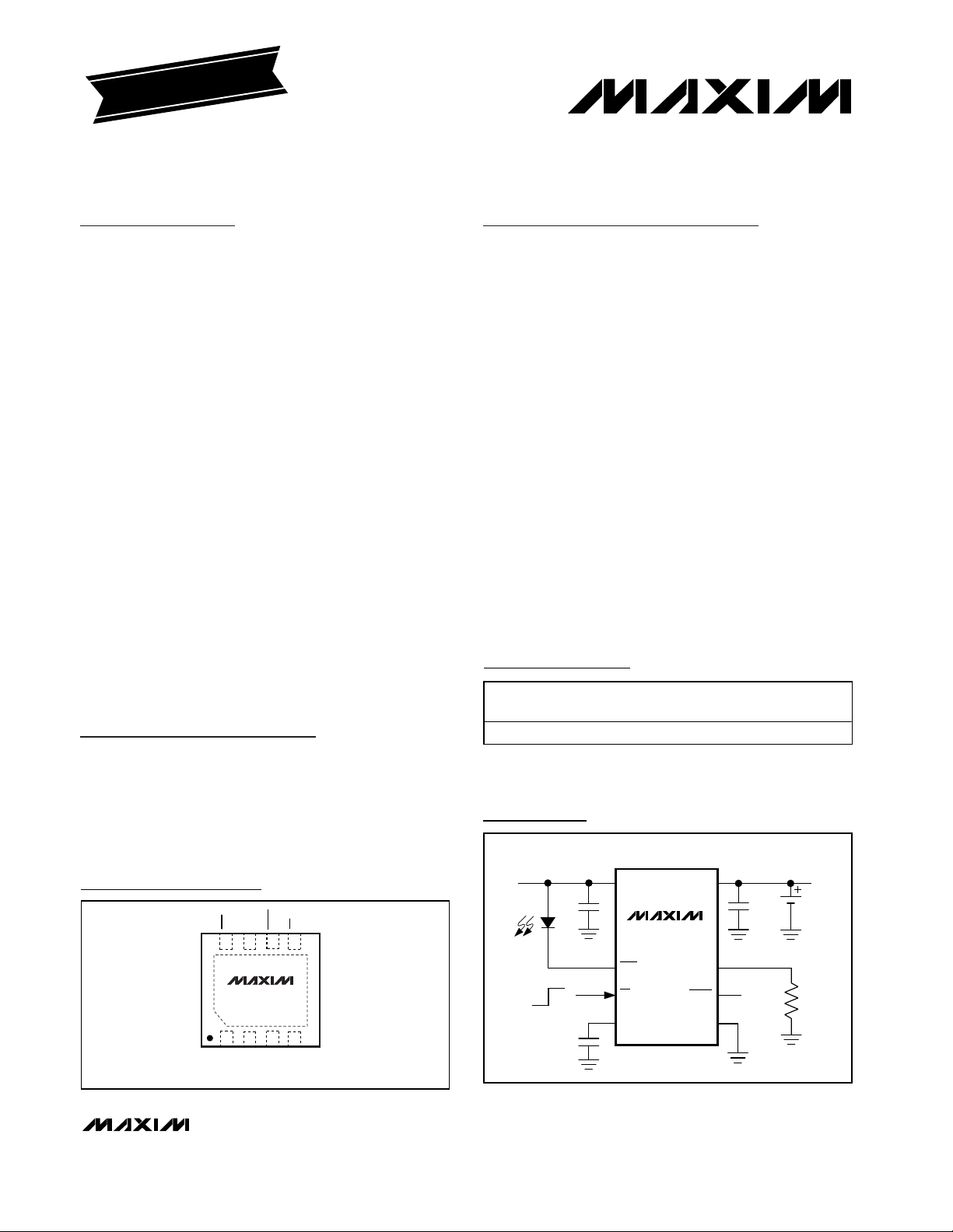
Pin Configuration
Ordering Information
Typical Operating Circuit
19-2890; Rev 0; 6/03
For pricing, delivery, and ordering information, please contact Maxim/Dallas Direct! at
1-888-629-4642, or visit Maxim’s website at www.maxim-ic.com.
EVALUATION KIT
AVAILABLE
Bluetooth is a trademark of Ericsson.
*EP = Exposed paddle.
TOP VIEW
EN
BATT
ACOK
CHG
8
76
5
PART TEMP RANGE PIN-PACKAGE
MAX1508ETA -40°C to +85°C 8 Thin DFN-EP* AHF
INPUT
4.25V TO 13V
1µF
IN
BATT
1µF
MAX1508
TOP
MARK
Li+
4.2V
MAX1508
3
2
1
IN
VL
3mm x 3mm THIN DFN
GND
OFF
ON
4
ISET
0.47µF
CHG
EN
VL
ISET
ACOK
GND
2.80kΩ
Page 2
MAX1508
Linear Li+ Battery Charger with Integrated Pass FET,
Thermal Regulation, and
ACOK
in 3mm x 3mm TDFN
2 _______________________________________________________________________________________
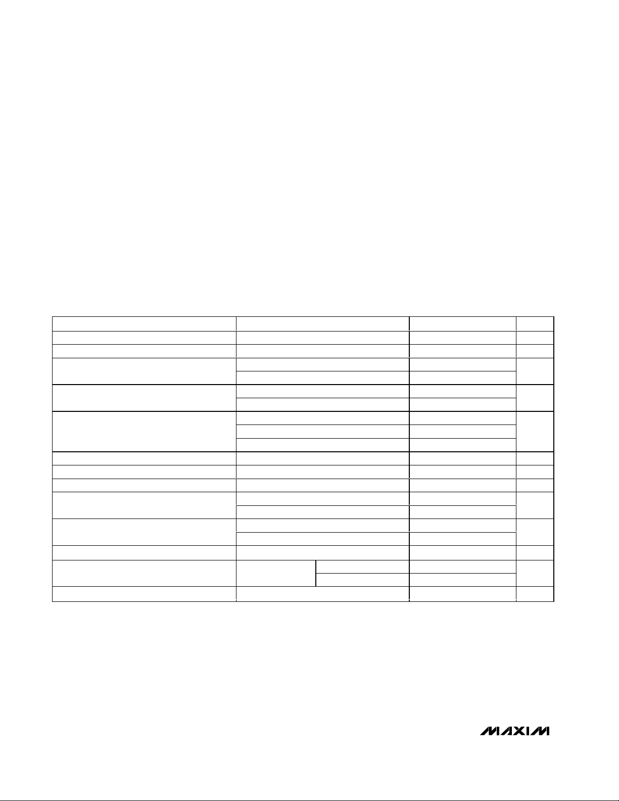
ABSOLUTE MAXIMUM RATINGS
ELECTRICAL CHARACTERISTICS
(VIN= 5V, V
BATT
= 4.0V, ACOK = EN = CHG = unconnected, R
ISET
= 2.8kΩ to GND, CVL= 0.47µF, BATT bypassed to GND with
1µF, T
A
= -40°C to +85°C, unless otherwise noted. Typical values are at TA= +25°C.) (Note 1)
Stresses beyond those listed under “Absolute Maximum Ratings” may cause permanent damage to the device. These are stress ratings only, and functional
operation of the device at these or any other conditions beyond those indicated in the operational sections of the specifications is not implied. Exposure to
absolute maximum rating conditions for extended periods may affect device reliability.
IN, CHG to GND .....................................................-0.3V to +14V
VL, BATT, ISET, EN, ACOK to GND .........................-0.3V to +6V
VL to IN...................................................................-14V to +0.3V
IN to BATT Continuous Current.............................................0.9A
Continuous Power Dissipation (T
A
= +70°C)
8-Pin TDFN (derate 24.4mW/°C above +70°C) .........1951mW
Short-Circuit Duration.................................................Continuous
Operating Temperature Range ...........................-40°C to +85°C
Junction Temperature......................................................+150°C
Storage Temperature Range .............................-65°C to +150°C
Lead Temperature (soldering, 10s) .................................+300°C
Input Voltage Range 013V
Input Operating Range 4.25 6.50 V
ACOK Trip Point, IN
Overvoltage Lockout Trip Point
VL Output Voltage IVL = 100µA 3.3 V
VL Load Regulation IVL = 100µA to 2mA -71 -200 mV
VL Temperature Coefficient IVL = 100µA -2 mV/°C
VL Undervoltage Lockout Trip Point
BATT Input Current
Maximum RMS Charge Current 0.8 A
Battery Regulation Voltage I
BATT Removal Detection Threshold V
PARAMETER CONDITIONS MIN TYP MAX UNITS
VIN - V
V
IN
VIN rising 6.5 7 7.5
V
IN
Charging (IIN - I
Disabled, EN = VL 0.8 1.5IN Input Current
OFF state (V
VIN rising 2.95
Hysteresis 0.17
V
IN
EN = VL 4 10
BATT
BATT
, VIN rising 20 40 60
BATT
- V
, VIN falling 15 30 45
BATT
hysteresis 0.11
IN
= 0 to 4V 3 10
= 0
rising 4.4 4.67 4.9 V
)12
BATT
= V
= 4.0V) 0.065
BATT
= 0°C to +85°C 4.162 4.2 4.238
T
A
= -40°C to +85°C 4.150 4.2 4.250
T
A
mV
V
mA
V
µA
V
Page 3
MAX1508
Li+ Linear Battery Charger with Integrated Pass FET,
Thermal Regulation, and
ACOK
in 3mm x 3mm TDFN
_______________________________________________________________________________________ 3
Note 1: Limits are 100% production tested at TA= +25°C. Limits over operating temperature range are guaranteed through correla-
tion using statistical quality control (SQC) methods.
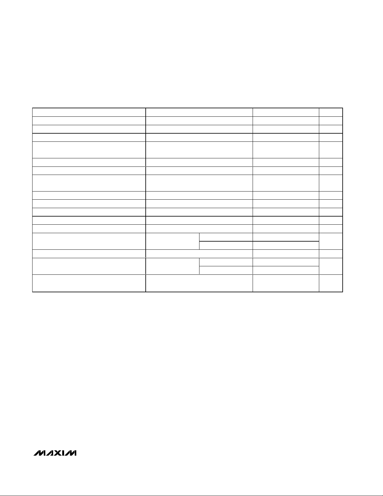
ELECTRICAL CHARACTERISTICS (continued)
(VIN= 5V, V
BATT
= 4.0V, ACOK = EN = CHG = unconnected, R
ISET
= 2.8kΩ to GND, CVL= 0.47µF, BATT bypassed to GND with
1µF, T
A
= -40°C to +85°C, unless otherwise noted. Typical values are at TA= +25°C.) (Note 1)
BATT Removal Detection-Threshold Hysteresis 200 mV
Minimum BATT Bypass Capacitance 1 µF/A
Fast-Charge Current-Loop System Accuracy V
Precharge Current System Accuracy
Die-Temperature-Regulation Set Point 100 °C
V
Precharge Threshold Voltage V
BATT
Current-Sense Amplifier Gain, I
Fast-Charge Mode
Regulator Dropout Voltage (V
EN Logic Input Low Voltage 4.25V < VIN < 6.5V 0.52 V
EN Logic Input High Voltage 4.25V < VIN < 6.5V 1.3 V
EN Internal Pulldown Resistor 100 200 400 kΩ
CHG Output Low Current V
CHG Output High Leakage Current V
ACOK Output Low Voltage I
ACOK Output High Leakage Current V
Full-Battery Detection Current Threshold
(as a Percentage of the Fast-Charge Current)
PARAMETER CONDITIONS MIN TYP MAX UNITS
= 3.5V 478 520 562 mA
BATT
Percentage of the fast-charge current,
= 2.2V
V
BATT
rising 2.3 2.5 2.7 V
BATT
IN
SET
- V
to I
BATT
in
BATT
)V
I
BATT
BATT
CHG
CHG
ACOK
ACOK
I
BATT
= 500mA, V
= 4.1V, I
= 1V 5 12 20 mA
= 13V
= 0.5mA 0.4 V
= 5.5V
falling 5 10 15 %
51015%
= 1.4V 0.880 0.958 1.035 mA/A
ISET
= 425mA 130 200 mV
BATT
TA = +25°C1
= +85°C 0.002
T
A
TA = +25°C1
= +85°C 0.002
T
A
µA
µA
Page 4
MAX1508
Linear Li+ Battery Charger with Integrated Pass FET,
Thermal Regulation, and
ACOK
in 3mm x 3mm TDFN
4 _______________________________________________________________________________________
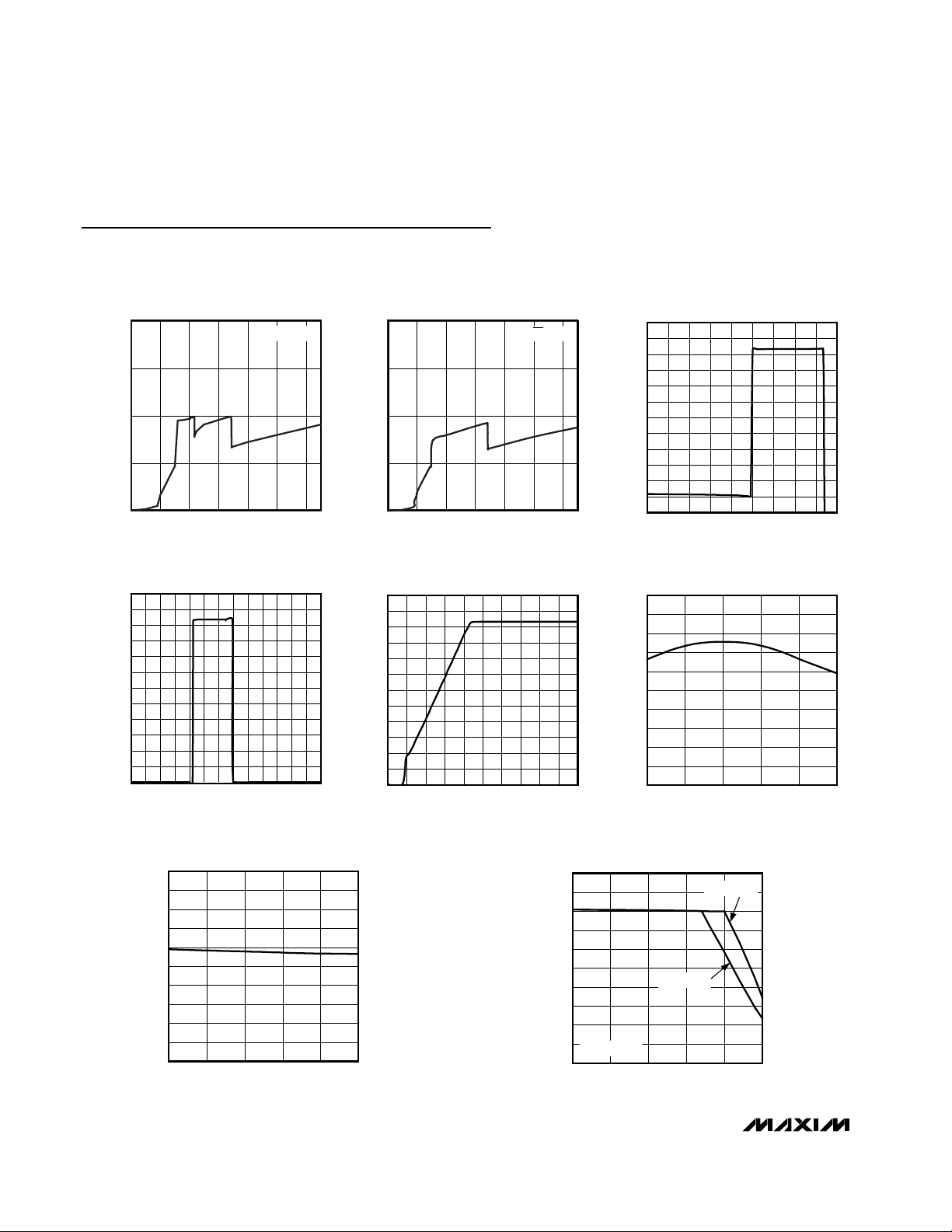
Typical Operating Characteristics
(VIN= 5V, V
BATT
= 4.0V, ACOK = EN = CHG = unconnected, R
ISET
= 2.8kΩ to GND, CIN= 1µF, C
BATT
= 1µF, CVL= 0.47µF, TA=
+25°C, unless otherwise noted.)
0
0.5
1.0
1.5
2.0
SUPPLY CURRENT
vs. INPUT VOLTAGE
MAX1508 toc01
INPUT VOLTAGE (V)
SUPPLY CURRENT (mA)
0
6
8
2
410
12
I
BATT
= 0
0
0.5
1.0
1.5
2.0
DISABLED-MODE SUPPLY
CURRENT vs. INPUT VOLTAGE
MAX1508 toc02
INPUT VOLTAGE (V)
DISABLED-MODE SUPPLY CURRENT (mA)
0
EN = VL
6
8
4210
12
0
250
150
450
350
550
200
100
400
300
500
600
02.01.0 3.0 4.00.5 2.51.5 3.5 4.5
CHARGE CURRENT
vs. BATTERY VOLTAGE
MAX1508 toc03
BATTERY VOLTAGE (V)
CHARGE CURRENT (mA)
0
50
250
150
450
350
550
200
100
400
300
500
600
06824 101217935 1113
CHARGE CURRENT
vs. INPUT VOLTAGE
MAX1508 toc04
INPUT VOLTAGE (V)
CHARGE CURRENT (mA)
0
200
100
400
300
500
50
250
150
450
350
550
600
0 0.160.08 0.24 0.400.04 0.200.12 0.28 0.32 0.36
CHARGE CURRENT
vs. INPUT-VOLTAGE HEADROOM
MAX1508 toc05
VIN - V
BATT
(V)
CHARGE CURRENT (mA)
4.180
4.186
4.198
4.192
4.204
4.189
4.183
4.201
4.195
4.207
4.210
-40 10-15 35 60 85
BATTERY REGULATION VOLTAGE
vs. TEMPERATURE
MAX1508 toc06
TEMPERATURE (°C)
BATTERY REGULATION VOLTAGE (V)
600
560
520
460
420
580
540
480
500
440
-40 10-15 35 60 85
CHARGE CURRENT
vs. AMBIENT TEMPERATURE
MAX1508 toc07
AMBIENT TEMPERATURE (°C)
CHARGE CURRENT (mA)
0
200
600
400
800
100
300
700
500
900
1000
-40 10-15 35 60 85
CHARGE CURRENT
vs. AMBIENT TEMPERATURE
MAX1508 toc09
AMBIENT TEMPERATURE (°C)
CHARGE CURRENT (mA)
V
BATT
= 4.0V
V
BATT
= 3.6V
R
ISET
= 1.87kΩ
Page 5
MAX1508
Li+ Linear Battery Charger with Integrated Pass FET,
Thermal Regulation, and
ACOK
in 3mm x 3mm TDFN
_______________________________________________________________________________________ 5
Pin Description
Detailed Description
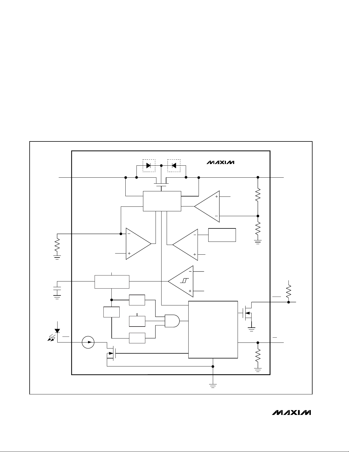
The MAX1508 charger uses voltage, current, and thermal-control loops to charge a single Li+ cell and to protect the battery (Figure 1). When a Li+ battery with a cell
voltage below 2.5V is inserted, the MAX1508 charger
enters the prequalification stage where it precharges that
cell with 10% of the user-programmed fast-charge current. The CHG indicator output is driven low (Figure 2) to
indicate entry into the prequalification state. Once the
cell has passed 2.5V, the charger soft-starts before it
enters the fast-charge stage. The fast-charge current
level is programmed through a resistor from ISET to
ground. As the battery voltage approaches 4.2V, the
charging current is reduced. If the battery current drops
to less than 10% of the fast-charging current, the CHG
indicator goes high impedance, signaling the battery is
fully charged. At this point the MAX1508 enters a constant voltage-regulation mode to maintain the battery at
full charge. If, at any point while charging the battery, the
die temperature approaches +100°C, the MAX1508
reduces the charging current so the die temperature
does not exceed the temperature-regulation set point.
The thermal-regulation loop limits the MAX1508 die
temperature to +100°C by reducing the charge current
as necessary (see the Thermal Regulation section).
This feature not only protects the MAX1508 from overheating, but also allows higher charge current without
risking damage to the system.
EN
Charger Enable Input
EN is a logic input (active low) to enable the charger.
Drive EN low, leave floating, or connect to GND to
enable the charger control circuitry. Drive EN high to
disable the charger control circuitry. EN has a 200kΩ
internal pulldown resistance.
ACOK
Output
Active-Low Output. The open-drain ACOK output
asserts low when +4.25V < VIN< +7V and VIN- V
BATT
> 40mV. ACOK requires an external 100kΩ pullup
resistor to the system’s logic I/O voltage. ACOK is high
impedance in shutdown.
VL Internal Voltage Regulator
The MAX1508 linear charger contains an internal linear
regulator available on the VL output pin. VL requires a
0.47µF ceramic bypass capacitor to GND. VL is regulated to 3.3V whenever the input voltage is above 3.5V.
PIN NAME FUNCTION
1 VL Internally Generated Logic Supply for Chip. Bypass VL to GND with a 0.47µF capacitor.
2 IN Input Supply Voltage. Bypass IN to GND with a 1µF capacitor to improve line noise and transient rejection.
3 GND Ground. Connect GND and exposed pad to a large copper trace for maximum power dissipation.
Charge-Current Program and Fast-Charge Current Monitor. Output current from ISET is 0.958mA per amp of
4 ISET
5 EN
6 ACOK
7 BATT Li+ Battery Connection. Bypass BATT to GND with a capacitor of at least 1µF per ampere of charge current.
8 CHG
— PAD
battery charging current. The charging current is set by connecting a resistor from ISET to GND. Fast-charge
current = 1461V / R
Logic-Level Enable Input. Drive EN high to disable charger. Pull EN low or float for normal operation. EN has
an internal 200kΩ pulldown resistor.
Input Power-Detection Output. The open-drain ACOK output asserts low when +4.25V
V
> 40mV. ACOK requires an external 100kΩ pullup resistor. ACOK is high impedance in shutdown.
BATT
Charging Indicator, Open-Drain Output. CHG goes low (and can turn on an LED) when charging begins.
CHG is high impedance when the battery current drops below 10% of the fast-charging current, or when EN
is high. Connect a pullup resistor to the µP’s I/O voltage when interfacing with a µP logic input.
Exposed Pad. Connect exposed pad to a large copper trace for maximum power dissipation. The pad is
internally connected to GND.
ISET
Ω.
< VIN < +7V and VIN -
Page 6
MAX1508
Linear Li+ Battery Charger with Integrated Pass FET,
Thermal Regulation, and
ACOK
in 3mm x 3mm TDFN
6 _______________________________________________________________________________________
CHG
Charge Indicator Output
CHG is an open-drain current source for indicating
charge status. Table 1 describes the state of CHG during different stages of operation.
CHG is a nominal 12mA current source suitable for driving a charge-indication LED. If the MAX1508 is used
in conjunction with a microprocessor, a pullup resistor
to the logic I/O voltage allows CHG to indicate charge
status to the µP instead of driving an LED.
Soft-Start
An analog soft-start algorithm activates when entering
fast-charge mode. When the prequalification state is
complete (V
BATT
exceeds +2.5V), the charging current
ramps up in 3ms to the full charging current. This
reduces the inrush current on the input supply.
Figure 1. Functional Diagram
IN
ISET
OUTPUT DRIVER,
CURRENT SENSE,
AND LOGIC
MAX1508
TEMPERATURE
SENSOR
V
REF
BATT
VL
0.47µF
CHG
IREF
IN
VL
V
LUVLO
REF
N
IN
V
INOVLO
REFOK
INOK
V
LOK
REFOK
ON
100°C
IN
VI/O
BATT
ACOK
N
LOGIC
EN
200kΩ
GND
Page 7
MAX1508
Li+ Linear Battery Charger with Integrated Pass FET,
Thermal Regulation, and
ACOK
in 3mm x 3mm TDFN
_______________________________________________________________________________________ 7
Applications Information
Charge-Current Selection
The maximum charging current is programmed by an
external R
ISET
resistor connected from ISET to GND.
Select the R
ISET
value based on the following formula:
I
FAST
= 1461V / R
ISET
Ω
where I
FAST
is in amps and R
ISET
is in ohms. ISET can
also be used to monitor the fast-charge current level.
The output current from the ISET pin is 0.958mA per
amp of charging current. The output voltage at ISET is
proportional to the charging current as follows:
V
ISET
= (I
CHG
x R
ISET
) / 1044
The voltage at ISET is nominally 1.4V at the selected
fast-charge current, and falls with charging current as
the cell becomes fully charged.
Thermal Regulation
The MAX1508 features a proprietary thermal-regulation
circuit to protect both the IC and the system from
excessive heat. When the MAX1508’s die temperature
reaches +100°C, the charge current is reduced to prevent any additional increase in the die temperature. An
active thermal loop does not indicate a fault condition.
Thermal regulation allows the MAX1508 to provide continuous charge to the battery under adverse conditions
without causing excessive power dissipation.
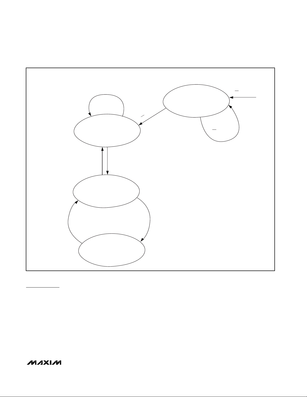
Figure 2. Charge State Diagram
< 2.5V
V
BATT
PRECHARGE
100% CHARGE CURRENT
V
< 2.4V
BATT
FAST CHARGE
100% CHARGER CURRENT
LED = ON
LED = ON
V
BATT
> 2.5V
IN
V
V
AND
< 7V AND
BATT
> V
IN
EN = LOW
ASYNCHRONOUS FROM
ANYWHERE
> 7V +
V
IN
> VIN +
V
BATT
SHUTDOWN
CHARGER = OFF
LED = OFF
V
> 7V +
IN
V
BATT
EN = HIGH
EN = HIGH
> VIN +
I
> 20%
CHARGE
OF ISET
FULL BATT
LED = OFF
< 10%
I
CHARGE
OF ISET
FULL BATT CONTINUES
TO REGULATE BATT
UP TO 4.2V
Page 8

MAX1508
Linear Li+ Battery Charger with Integrated Pass FET,
Thermal Regulation, and
ACOK
in 3mm x 3mm TDFN
8 _______________________________________________________________________________________
X = Don’t care.
*I
FAST
is reduced as necessary to maintain the die temperature at +100°C.
Table 1. CHG States
Capacitor Selection
Connect a ceramic capacitor from BATT to GND for
proper stability. Use a 1µF X5R ceramic capacitor for
most applications.
Connect a 1µF ceramic capacitor from IN to GND. Use
a larger input bypass capacitor for high input voltages
or high charging currents to reduce supply noise.
Connect a 0.47µF ceramic capacitor from VL to GND.
Thermal Considerations
The MAX1508 is in a thermally enhanced thin DFN package with exposed paddle. Connect the exposed paddle
of the MAX1508 to a large copper ground plane to provide a thermal contact between the device and the circuit
board. The exposed paddle transfers heat away from the
device, allowing the MAX1508 to charge the battery with
maximum current, while minimizing the increase in die
temperature.
DC Input Sources
The MAX1508 operates from well-regulated DC
sources. The full-charging input voltage range is 4.25V
to 7V. The device can stand up to 13V on the input
without damage to the IC. If VINis greater than 7V, then
the MAX1508 stops charging.
An appropriate power supply must provide at least
4.25V when sourcing the desired peak charging current. It also must stay below 6.5V when unloaded.
Application Circuits
Stand-Alone Li+ Charger
The MAX1508 provides a complete Li+ charging solution. The Typical Operating Circuit on the front page
shows the MAX1508 as a stand-alone Li+ battery
charger. The 2.8kΩ resistor connected to ISET sets a
charging current of 520mA. The LED indicates when
either fast-charge or precharge qualification has
begun. When the battery is full, the LED turns off.
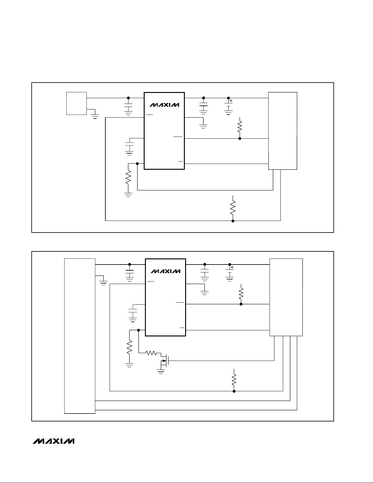
Microprocessor-Interfaced Charger
Figure 3 shows the MAX1508 as a µP-cooperated Li+
battery charger. The MAX1508 starts charging the battery when EN is low. The µP can drive EN high to disable the charger. The MAX1508’s ACOK output
indicates the presence of a valid AC adapter to the µP.
CHG can be used to detect the charge status of a battery. By monitoring V
ISET
, the system can measure the
charge current.
USB-Powered Li+ Charger
The universal serial bus (USB) provides a high-speed
serial communication port as well as power for the
remote device. The MAX1508 can be configured to
charge its battery at the highest current possible from
the host port. Figure 4 shows the MAX1508 as a USB
battery charger. To make the circuit compatible with
either 100mA or 500mA USB ports, the circuit initializes
at 95mA charging current. The microprocessor then
interrogates the host to determine its current capability.
If the host port is capable, the charging current is
increased to 435mA. The 435mA current was chosen to
avoid exceeding the 500mA USB specification.
Layout and Bypassing
Connect a 1µF ceramic input capacitor as close to the
device as possible. Provide a large copper GND plane
to allow the exposed paddle to sink heat away from the
device. Connect the battery to BATT as close to the
device as possible to provide accurate battery voltage
sensing. Make all high-current traces short and wide to
minimize voltage drops. For an example layout, refer to
the MAX1507/MAX1508 evaluation kit layout.
Chip Information
TRANSISTOR COUNT: 1812
PROCESS: BiCMOS
EN V
XV
Low 4.25V ≤ VIN ≤ 7V < 2.5V 10% of I
Low 4.25V ≤ VIN ≤ 7V ≥ 2.5V I
Low 4.25V ≤ VIN ≤ 7V 4.2V 10% of I
Low >7V X 0 Hi-Z Overvoltage
High X X 0 Hi-Z Disabled
IN
BATT
V
BATT
V
IN
I
BATT
0 Hi-Z Shutdown
FAST
* Low Fast Charge
FAST
FAST
CHG STATE
Low Prequalification
Hi-Z Full Charge
Page 9
MAX1508
Li+ Linear Battery Charger with Integrated Pass FET,
Thermal Regulation, and
ACOK
in 3mm x 3mm TDFN
_______________________________________________________________________________________ 9
Figure 3. µP-Interfaced Li+ Battery Charger
Figure 4. USB Battery Charger
AC/DC
ADAPTER
1µF
0.47µF
2.8kΩ
IN
MAX1508
CHG
VL
ISET
BATT
1µF
GND
ACOK
EN
CHARGE-CURRENT MONITOR
LOW: CHARGE, HIGH: FULL OR OFF
4.2V Li+
VI/O
SYSTEM
VI/O
VBUS
GND
USB PORT
D+
D-
1µF
0.47µF
15.4kΩ
IN
CHG
VL
ISET
4.3kΩ
MAX1508
N
BATT
1µF
GND
ACOK
EN
HIGH: 435mA, LOW: 95mA
4.2V Li+
VI/O
SYSTEM
VI/O
Page 10

MAX1508
Linear Li+ Battery Charger with Integrated Pass FET,
Thermal Regulation, and
ACOK
in 3mm x 3mm TDFN
10 ______________________________________________________________________________________
Package Information
(The package drawing(s) in this data sheet may not reflect the most current specifications. For the latest package outline information
go to www.maxim-ic.com/packages
.)
PIN 1
INDEX
AREA
D
A
A2
b
E
A1
L
DETAIL A
E2
e
C
L
C0.35
D2
C
L
L
PIN 1 ID
1N1
[(N/2)-1] x e
REF.
k
L
6, 8, &10L, QFN THIN.EPS
A
NUMBER OF LEADS SHOWN ARE FOR REFERENCE ONLY
e
PROPRIETARY INFORMATION
TITLE:
PACKAGE OUTLINE, 6, 8 & 10L,
TDFN, EXPOSED PAD, 3x3x0.80 mm
APPROVAL
e
DALLAS
SEMICONDUCTOR
DOCUMENT CONTROL NO. REV.
21-0137 D
1
2
Page 11
MAX1508
Li+ Linear Battery Charger with Integrated Pass FET,
Thermal Regulation, and
ACOK
in 3mm x 3mm TDFN
Maxim cannot assume responsibility for use of any circuitry other than circuitry entirely embodied in a Maxim product. No circuit patent licenses are
implied. Maxim reserves the right to change the circuitry and specifications without notice at any time.
Maxim Integrated Products, 120 San Gabriel Drive, Sunnyvale, CA 94086 408-737-7600 ____________________ 11
© 2003 Maxim Integrated Products Printed USA is a registered trademark of Maxim Integrated Products.
Package Information (continued)
(The package drawing(s) in this data sheet may not reflect the most current specifications. For the latest package outline information
go to www.maxim-ic.com/packages
.)
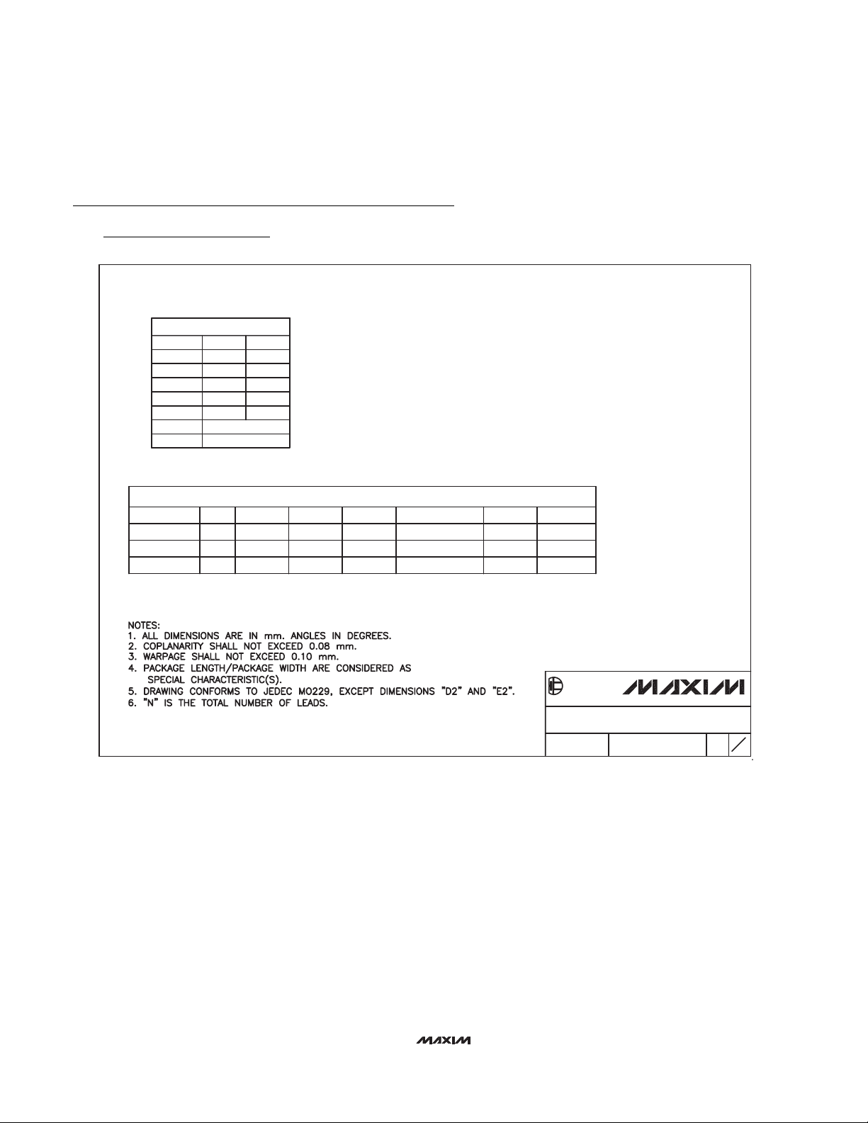
COMMON DIMENSIONS
SYMBOL
A
D
E
A1
L
k
A2 0.20 REF.
PACKAGE VARIATIONS
PKG. CODE
T633-1 1.50–0.10D22.30–0.10
MIN. MAX.
0.70 0.80
2.90 3.10
2.90 3.10
0.00 0.05
0.20 0.40
0.25 MIN.
N
6
1.50–0.10
E2
0.95 BSCeMO229 / WEEA
2.30–0.10T833-1 8
0.65 BSC
JEDEC SPEC
MO229 / WEEC
[(N/2)-1] x e
0.40–0.05b1.90 REF
1.95 REF0.30–0.05
0.25–0.05 2.00 REFMO229 / WEED-30.50 BSC1.50–0.10 2.30–0.1010T1033-1
DALLAS
SEMICONDUCTOR
PROPRIETARY INFORMATION
TITLE:
PACKAGE OUTLINE, 6, 8 & 10L,
TDFN, EXPOSED PAD, 3x3x0.80 mm
DOCUMENT CONTROL NO.APPROVAL
21-0137
REV.
2
2
D
 Loading...