

Page 1
19-5478; Rev 2; 7/11
EVALUATION KIT
AVAILABLE
High-Efficiency, 3A, Current-Mode
Synchronous, Step-Down Switching Regulator
General Description
The MAX15058 high-efficiency, current-mode, synchronous step-down switching regulator with integrated
power switches delivers up to 3A of output current.
The device operates from 2.7V to 5.5V and provides an
output voltage from 0.6V up to 94% of the input voltage,
making the device ideal for distributed power systems,
portable devices, and preregulation applications.
The MAX15058 utilizes a current-mode control architecture with a high-gain transconductance error amplifier. The current-mode control architecture facilitates
easy compensation design and ensures cycle-by-cycle
current limit with fast response to line and load transients.
The MAX15058 offers selectable skip-mode functionality to reduce current consumption and achieve a higher
efficiency at light output load. The low R
DS(ON)
integrated switches ensure high efficiency at heavy loads
while minimizing critical inductances, making the layout
design a much simpler task with respect to discrete
solutions. Utilizing a simple layout and footprint assures
first-pass success in new designs.
The MAX15058 features a 1MHz, factory-trimmed, fixedfrequency PWM mode operation. The high switching frequency, along with the PWM current-mode architecture,
allows for a compact, all-ceramic capacitor design.
The MAX15058 offers a capacitor-programmable softstart reducing inrush current, startup into PREBIAS
operations, and a PGOOD open-drain output that can be
used as an interrupt and for power sequencing.
The MAX15058 is available in a 9-bump (3 x 3 array),
1.5mm x 1.5mm WLP package and is specified over the
-40NC to +85NC temperature range.
Applications
Distributed Power Systems
Preregulators for Linear Regulators
Portable Devices
Notebook Power
Server Power
IP Phones
Features
S Internal 30mI (typ) R
DS(ON)
(typ) Low-Side MOSFETs at 5V
S Continuous 3A Output Current Over Temperature
S 95% Efficiency with 3.3V Output at 3A
S 1% Output Voltage Accuracy Over Load, Line, and
Temperature
S Operates from 2.7V to 5.5V Supply
S Cycle-by-Cycle Overcurrent Protection
S Adjustable Output from 0.6V to Up to 0.94 x V
S Programmable Soft-Start
S Factory-Trimmed, 1MHz Switching Frequency
S Stable with Low-ESR Ceramic Output Capacitors
S Safe-Startup Into Prebiased Output
S External Reference Input
S Skip-Mode Functionality
S Enable Input/Power-Good Output
S Fully Protected Against Overcurrent and
Overtemperature
S Input Undervoltage Lockout
High-Side and 18mI
Ordering Information
PART TEMP RANGE PIN-PACKAGE
MAX15058EWL+ -40°C to +85°C 9 WLP
+Denotes a lead(Pb)-free/RoHS-compliant package.
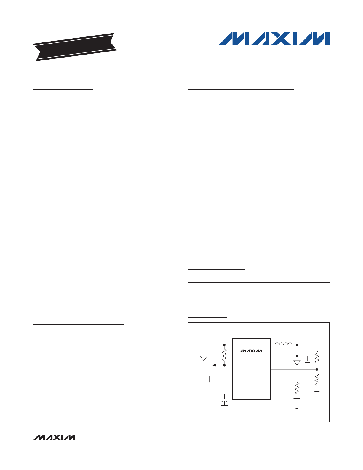
Typical Operating Circuit
INPUT
2.8V TO 5.5V
ENABLE
OFF
ON
IN LX
MAX15058
PGOOD
EN
SKIP
SS/REFIN
GND
COMP
FB
IN
OUTPUT
1.8V/3A
MAX15058
_______________________________________________________________ Maxim Integrated Products 1
For pricing, delivery, and ordering information, please contact Maxim Direct at 1-888-629-4642,
or visit Maxim’s website at www.maxim-ic.com.
Page 2
High-Efficiency, 3A, Current-Mode
Synchronous, Step-Down Switching Regulator
ABSOLUTE MAXIMUM RATINGS
IN, PGOOD to GND ................................................-0.3V to +6V
LX to GND ..................................................-0.3V to (VIN + 0.3V)
LX to GND .......................................-1V to (VIN + 0.3V) for 50ns
EN, COMP, FB, SS/REFIN, SKIP to GND ...-0.3V to (VIN + 0.3V)
LX Current (Note 1) ................................................... -6A to +6A
Output Short-Circuit Duration ....................................Continuous
Note 1: LX has internal clamp diodes to GND and IN. Applications that forward bias these diodes should not exceed the IC’s pack-
MAX15058
age power dissipation limits.
PACKAGE THERMAL CHARACTERISTICS (Note 2)
WLP
Junction-to-Case Thermal Resistance (BJC) ...................26NC/W
Junction-to-Ambient Thermal Resistance (BJA) .............. 71NC/W
Note 2: Package thermal resistances were obtained using the method described in JEDEC specification JESD51-7, using a four-
layer board. For detailed information on package thermal considerations, refer to www.maxim-ic.com/thermal-tutorial.
ELECTRICAL CHARACTERISTICS
(VIN = 5V, TA = -40NC to +85NC, unless otherwise noted. Typical values are at TA = +25NC.) (Note 3)
PARAMETER SYMBOL CONDITIONS MIN TYP MAX UNITS
IN Voltage Range V
IN Shutdown Supply Current VEN = 0V 0.2 2
IN Supply Current I
V
Undervoltage Lockout
IN
Threshold
V
Undervoltage Lockout
IN
Hysteresis
ERROR AMPLIFIER
Transconductance g
Voltage Gain A
FB Set-Point Accuracy V
FB Input Bias Current I
COMP to Current-Sense
Transconductance
COMP Clamp Low VFB = 0.65V, VSS = 0.6V 0.94 V
POWER SWITCHES
LX On-Resistance, High-Side
pMOS
LX On-Resistance, Low-Side
nMOS
High-Side Switch Current-Limit
Threshold
Low-Side Switch Sink CurrentLimit Threshold
Low-Side Switch Source CurrentLimit Threshold
IN
MV
VEA
FB
FB
g
MC
I
HSCL
IN
VEN = 5V, VFB = 0.65V, no switching 1.56 2.3 mA
LX starts switching, VIN rising 2.6 2.7 V
LX stops switching, VIN falling 200 mV
Over line, load, and temperature 594 600 606 mV
VFB = 0.6V -500 +500 nA
Continuous Power Dissipation (TA = +70NC)
9-Bump WLP Multilayer Board
(derate 14.1mW/NC above TA = +70NC) .................... 1127mW
Operating Temperature Range .......................... -40NC to +85NC
Storage Temperature Range ............................ -65NC to +150NC
Soldering Temperature (reflow) ......................................+260NC
2.7 5.5 V
1.5 mS
90 dB
18 A/V
30
18
5 A
4 A
5 A
FA
mI
mI
2 ______________________________________________________________________________________
Page 3
High-Efficiency, 3A, Current-Mode
Synchronous, Step-Down Switching Regulator
ELECTRICAL CHARACTERISTICS (continued)
(VIN = 5V, TA = -40NC to +85NC, unless otherwise noted. Typical values are at TA = +25NC.) (Note 3)
PARAMETER SYMBOL CONDITIONS MIN TYP MAX UNITS
LX Leakage Current VEN = 0V 10
RMS LX Output current 3 A
OSCILLATOR
Switching Frequency f
Maximum Duty Cycle D
Minimum Controllable On-Time 70 ns
Slope Compensation Ramp
Valley
Slope Compensation Ramp
Amplitude
ENABLE
EN Input High Threshold Voltage VEN rising 1.45 V
EN Input Low Threshold Voltage VEN falling 0.4 V
EN Input Leakage Current VEN = 5V 0.025
SKIP Input Leakage Current V
SOFT-START, PREBIAS, REFIN
Soft-Start Current I
SS/REFIN Discharge Resistance R
SS/REFIN Prebias Mode Stop
Voltage
External Reference Input Range 0 IN - 1.8 V
HICCUP
Number of Consecutive CurrentLimit Events to Hiccup
Timeout 1024
POWER-GOOD OUTPUT
PGOOD Threshold VFB rising 0.535 0.555 0.575 V
PGOOD Threshold Hysteresis VFB falling 28 mV
PGOOD V
PGOOD Leakage V
THERMAL SHUTDOWN
Thermal Shutdown Threshold 150
Thermal Shutdown Hysteresis Temperature falling 20
Note 3: Specifications are 100% production tested at TA = +25NC. Limits over the operating temperature range are guaranteed by
OL
design and characterization.
SW
MAX
V
SLOPE
SS
Extrapolated to 100% duty cycle 320 mV
= VEN = 5V 25
SKIP
SS
V
SS/REFIN
I
SS/REFIN
V
SS/REFIN
I
PGOOD
PGOOD
= 0.45V, sourcing 10
= 10mA, sinking 8.3
rising 0.58 V
= 5mA, VFB = 0.5V 20 60 mV
= 5V, VFB = 0.65V 0.013
850 1000 1150 kHz
94 %
1.15 V
8 Events
FA
FA
FA
FA
I
Clock
Cycles
FA
NC
NC
MAX15058
_______________________________________________________________________________________ 3
Page 4
High-Efficiency, 3A, Current-Mode
Synchronous, Step-Down Switching Regulator
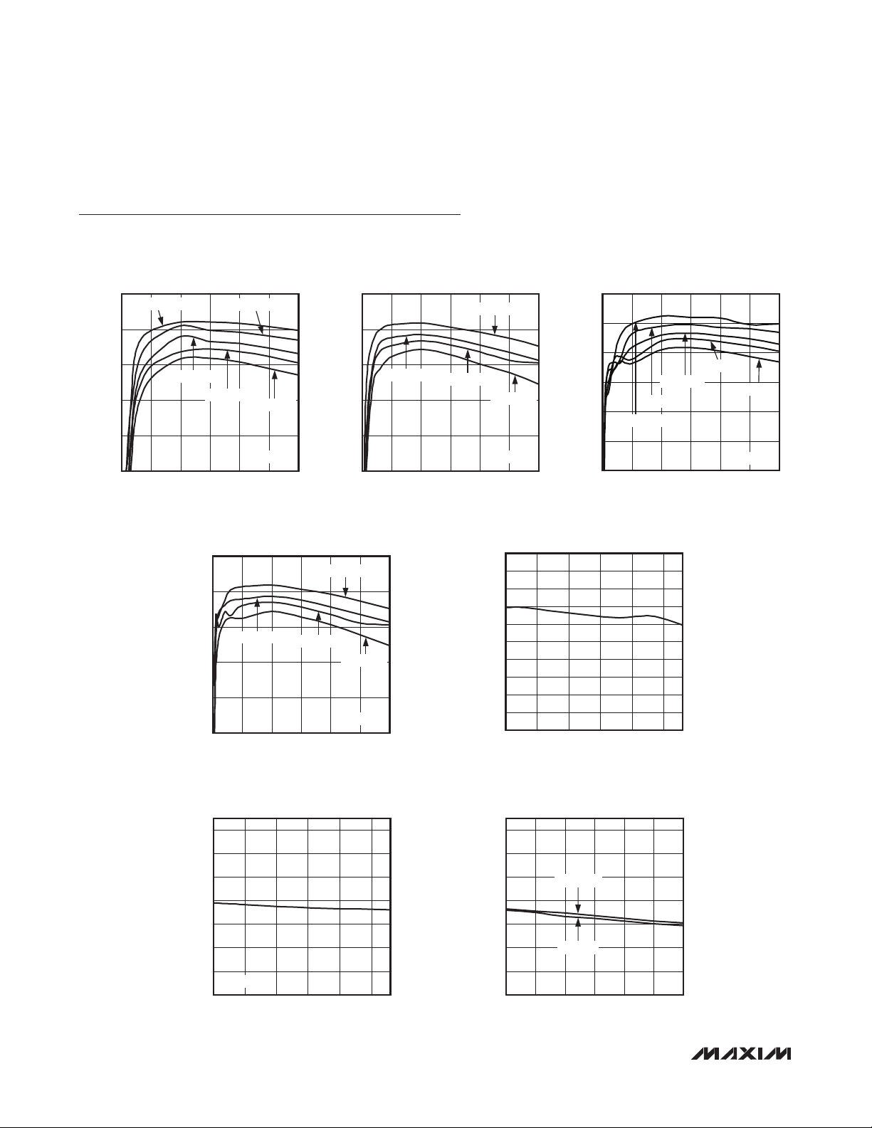
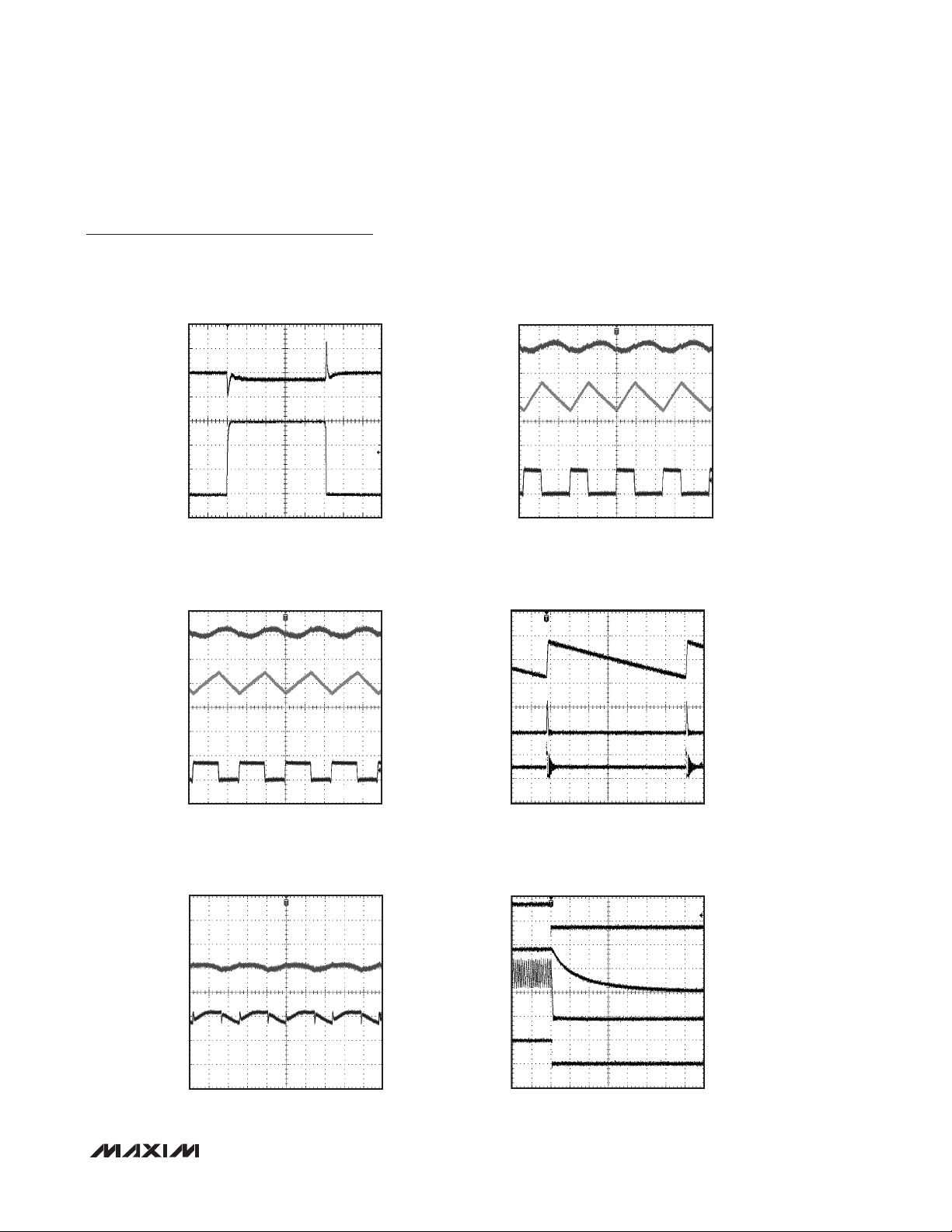
Typical Operating Characteristics
(VIN = 5V, V
OUT
= 1.8V, I
= 3A, Circuit of Figure 5, TA = +25NC, unless otherwise noted.)
LOAD
EFFICIENCY vs. LOAD CURRENT
(PWM MODE)
100
V
= 3.3V
OUT
95
MAX15058
90
85
EFFICIENCY (%)
80
75
0 3.0
V
= 1.8V
OUT
V
OUTPUT CURRENT (A)
100
95
90
85
EFFICIENCY (%)
80
75
EFFICIENCY vs. OUTPUT CURRENT
MAX15058 toc01
100
95
90
85
EFFICIENCY (%)
80
75
0 3.0
OUT
V
= 1.5V
OUT
= 2.5V
V
OUT
VIN = 5V
2.52.01.51.00.5
= 1.2V
EFFICIENCY vs. OUTPUT CURRENT
(SKIP MODE)
V
= 2.5V
OUT
V
= 1.8V
OUT
0 3.0
V
= 1.5V
OUT
OUTPUT CURRENT (A)
V
= 1.2V
OUT
VIN = 3.3V
2.52.01.51.00.5
(FORCED PWM)
V
= 1.8V
OUT
OUTPUT CURRENT (A)
MAX15058 toc04
V
= 2.5V
OUT
V
= 1.5V
OUT
V
= 1.2V
OUT
VIN = 3.3V
2.52.01.51.00.5
1100
1080
1060
1040
1020
1000
980
960
SWITCHING FREQUENCY (kHz)
940
920
900
2.7 3.2 3.7 4.74.2 5.2
EFFICIENCY vs. LOAD CURRENT
100
95
MAX15058 toc02
90
85
EFFICIENCY (%)
80
V
OUT
75
70
0 3.0
SWITCHING FREQUENCY
vs. INPUT VOLTAGE
INPUT VOLTAGE (V)
(SKIP MODE)
V
= 1.8V
OUT
V
= 2.5V
OUT
= 3.3V
OUTPUT CURRENT (A)
MAX15058 toc05
MAX15058 toc03
V
= 1.5V
OUT
V
= 1.2V
OUT
VIN = 5V
2.52.01.51.00.5
OUTPUT VOLTAGE
vs. SUPPLY VOLTAGE
1.89
1.87
1.85
1.83
1.81
OUTPUT VOLTAGE (V)
1.79
1.77
I
= 0.5A
OUT
1.75
2.7 3.2 3.7 4.74.2 5.2
SUPPLY VOLTAGE (V)
MAX15058 toc06
1.89
1.87
1.85
1.83
1.81
OUTPUT VOLTAGE (V)
1.79
1.77
1.75
0 0.5 1.0 2.01.5 2.5 3.0
OUTPUT VOLTAGE
vs. OUTPUT CURRENT
V
= 3.3V
OUT
V
= 5V
OUT
OUTPUT CURRENT (A)
4 ______________________________________________________________________________________
MAX15058 toc07
Page 5
High-Efficiency, 3A, Current-Mode
Synchronous, Step-Down Switching Regulator
Typical Operating Characteristics (continued)
(VIN = 5V, V
OUT
= 1.8V, I
= 3A, Circuit of Figure 5, TA = +25NC, unless otherwise noted.)
LOAD
MAX15058
50mV/div
AC-COUPLED
1A/div
LOAD-TRANSIENT RESPONSE
100µs/div
SWITCHING WAVEFORMS (I
0A
400ns/div
MAX15058 toc08
= 3A)
OUT
MAX15058 toc09b
VIN = 3.3V
V
OUT
20mV/div
AC-COUPLED
I
LX
1AV/div
V
LX
5V/div
SWITCHING WAVEFORMS (I
0A
400ns/div
OUT
MAX15058 toc09a
SWITCHING WAVEFORM IN SKIP MODE
= 10mA)
(I
OUT
10
µs/div
MAX15058 toc10
= 3A)
V
OUT
20mV/div
AC-COUPLED
I
LX
1AV/div
V
LX
5V/div
V
OUT
50mV/div
AC-COUPLED
I
LX
1A/div
V
LX
5V/div
INPUT AND OUTPUT
WAVEFORMS (I
400ns/div
OUT
= 3A)
MAX15058 toc11
INPUT
20mV/div
AC-COUPLED
OUTPUT
100mV/div
AC-COUPLED
SHUTDOWN WAVEFORM
10
µs/div
MAX15058 toc12
V
ENABLE
5V/div
V
OUT
1V/div
I
LX
1A/div
V
PGOOD
5V/div
_______________________________________________________________________________________ 5
Page 6
High-Efficiency, 3A, Current-Mode
Synchronous, Step-Down Switching Regulator
Typical Operating Characteristics (continued)
(VIN = 5V, V
OUT
= 1.8V, I
= 3A, Circuit of Figure 5, TA = +25NC, unless otherwise noted.)
LOAD
MAX15058
100
90
80
70
60
50
40
30
SHUTDOWN CURRENT (nA)
20
10
0
2.7
SOFT-START WAVEFORMS
(PWM MODE) (I
200µs/div
SHUTDOWN CURRENT
vs. INPUT VOLTAGE
VEN = 0V
INPUT VOLTAGE (V)
OUT
= 3A)
MAX15058 toc13a
5.24.74.23.73.2
V
ENABLE
5V/div
V
OUT
1V/div
I
LX
1A/div
V
PGOOD
5V/div
MAX15058 toc14
SOFT-START WAVEFORMS
(SKIP MODE) (I
200µs/div
SHORT-CIRCUIT HICCUP MODE
200µs/div
OUT
= 3A)
MAX15058 toc13b
MAX15058 toc15
V
ENABLE
5V/div
V
OUT
1V/div
I
LX
1A/div
V
PGOOD
5V/div
I
IN
500mA/div
V
OUT
200mV/div
I
OUT
5A/div
RMS INPUT CURRENT
200
vs. INPUT VOLTAGE
160
120
80
RMS INPUT CURRENT (mA)
40
0
2.8 5.5
SHORT CIRCUIT ON OUTPUT
INPUT VOLTAGE (V)
MAX15058 toc16
FEEDBACK VOLTAGE (V)
5.24.94.64.34.03.73.43.1
FB VOLTAGE vs. TEMPERATURE
606
604
602
600
598
596
594
-40
AMBIENT TEMPERATURE (°C)
MAX15058 toc17
NO LOAD
806040200-20
6 ______________________________________________________________________________________
Page 7
High-Efficiency, 3A, Current-Mode
Synchronous, Step-Down Switching Regulator
Typical Operating Characteristics (continued)
(VIN = 5V, V
OUT
= 1.8V, I
= 3A, Circuit of Figure 5, TA = +25NC, unless otherwise noted.)
LOAD
MAX15058
SOFT-START WAVEFORMS
(EXTERNAL REFIN) (PWM MODE)
200
µs/div
MAX15058 toc18a
NO LOAD
STARTING INTO A PREBIASED OUTPUT
= 2A)
(I
OUT
MAX15058 toc19
V
SS/ REFIN
500mV/div
V
OUT
1V/div
I
LX
1A/div
V
PGOOD
5V/div
V
ENABLE
5V/div
V
OUT
1V/div
I
LX
1A/div
SOFT-START WAVEFORMS
(EXTERNAL REFIN) (SKIP MODE)
200
µs/div
MAX15058 toc18b
NO LOAD
STARTING INTO A PREBIASED OUTPUT
(NO LOAD)
MAX15058 toc20a
V
SS/ REFIN
500mV/div
V
OUT
1V/div
I
LX
1A/div
V
PGOOD
5V/div
V
ENABLE
5V/div
V
OUT
1V/div
I
LX
1A/div
V
1.8V
PGOOD
5V/div
V
OUT
500mV/div
I
L
1A/div
V
SS/REFIN
500mV/div
PWM MODE
200
µs/div
STARTING INTO A PREBIASED OUTPUT
SKIP MODE
(NO LOAD)
200
µs/div
MAX15058 toc20b
V
PGOOD
5V/div
V
ENABLE
5V/div
V
OUT
1V/div
I
LX
1A/div
V
PGOOD
5V/div
PWM MODE
200
µs/div
STARTING INTO A PREBIASED OUTPUT
HIGHER THAN SET OUTPUT
µs/div
400
MAX15058 toc21
10I LOAD AT OUT
_______________________________________________________________________________________ 7
Page 8
High-Efficiency, 3A, Current-Mode
Synchronous, Step-Down Switching Regulator
Typical Operating Characteristics (continued)
(VIN = 5V, V
OUT
= 1.8V, I
= 3A, Circuit of Figure 5, TA = +25NC, unless otherwise noted.)
LOAD
100
80
60
MAX15058
40
20
0
CASE TEMPERATURE (°C)
-20
-40
CASE TEMPERATURE
vs. AMBIENT TEMPERATURE
-40 80
AMBIENT TEMPERATURE (°C)
6040200-20
MAX15058 toc22
INPUT CURRENT IN SKIP MODE
vs. OUTPUT VOLTAGE
5.0
4.5
NO LOAD
4.0
3.5
3.0
2.5
2.0
INPUT CURRENT (mA)
1.5
1.0
0.5
0
1.2 1.7 2.2 2.7 3.2
VCC = 5.0V
VCC = 3.3V
OUTPUT VOLTAGE (V)
MAX15058 toc23
8 ______________________________________________________________________________________
Page 9

High-Efficiency, 3A, Current-Mode
Synchronous, Step-Down Switching Regulator
Pin Configuration
TOP VIEW
(BUMPS ON BOTTOM)
MAX15058
LXGND IN
A1
SKIPCOMP EN
B1
C1 C2 C3
B2 B3
SS/REFINFB PGOOD
WLP
Pin Description
BUMP NAME FUNCTION
A1 GND
A2 LX
A3 IN
B1 COMP
B2 SKIP Skip-Mode Input. Connect to EN to select skip mode or leave unconnected for normal operation.
B3 EN
C1 FB
C2 SS/REFIN
C3 PGOOD
Analog Ground/Low-Side Switch Source Terminal. Connect to the PCB copper plane at one point near
the input bypass capacitor return terminal.
Inductor Connection. Connect LX to the switched side of the inductor. LX is high impedance when the
IC is in shutdown mode.
Input Power Supply. Input supply range is from 2.7V to 5.5V. Bypass with a minimum 10FF ceramic
capacitor to GND. See Figures 5 and 6.
Voltage Error-Amplifier Output. Connect the necessary compensation network from COMP to GND. See
the Closing the Loop: Designing the Compensation Circuitry section.
Enable Input. EN is a digital input that turns the regulator on and off. Drive EN high to turn on the regulator. Connect to IN for always-on operation.
Feedback Input. Connect FB to the center tap of an external resistor-divider from the output to GND to
set the output voltage from 0.6V up to 94% of VIN.
Soft-Start/External Voltage Reference Input. Connect a capacitor from SS/REFIN to GND to set the startup
time. See the Setting the Soft-Start Time section for details on setting the soft-start time. Apply a voltage
reference from 0V to VIN - 1.5V to drive soft-start externally.
Open-Drain Power-Good Output. PGOOD goes high when FB is above 555mV and pulls low if FB is
below 527mV.
A3A2
MAX15058
_______________________________________________________________________________________ 9
Page 10

High-Efficiency, 3A, Current-Mode
Synchronous, Step-Down Switching Regulator
Block Diagram
SKIP
EN
IN
MAX15058
SS/REFIN
FB
BIAS
GENERATOR
VOLTAGE
REFERENCE
EN LOGIC, IN UVLO
THERMAL SHDN
STRONG PREBIASED
FORCED START
0.58V
SS/REFIN BUFFER
0.6V
ERROR AMPLIFIER
10µA
SHDN
C
SKPM
CK
PWM
COMPARATOR
SKIP-MODE
LOGIC
CONTROL
SKPM
CURRENT-SENSE
AMPLIFIER
IN
LOGIC
HIGH-SIDE
CURRENT LIMIT
LX
LX
IN
LX
IN
GND
LOW-SIDE SOURCE-SINK
CURRENT LIMIT AND ZERO-
CROSSING COMPARATOR
SINK
SOURCE
ZX
COMP
OSCILLATOR
RAMP GEN
0.555V RISING,
0.527V FALLING
RAMP
CK
POWER-GOOD
COMPARATOR
MAX15058
SKPM
10 _____________________________________________________________________________________
PGOOD
Page 11

High-Efficiency, 3A, Current-Mode
Synchronous, Step-Down Switching Regulator
Detailed Description
The MAX15058 high-efficiency, current-mode switching
regulator can deliver up to 3A of output current. The
MAX15058 provides output voltages from 0.6V to 0.94 x
VIN from 2.7V to 5.5V input supplies, making the device
ideal for on-board point-of-load applications.
The MAX15058 delivers current-mode control architecture using a high-gain transconductance error
amplifier. The current-mode control architecture facilitates
easy compensation design and ensures cycle-by-cycle
current limit with fast response to line and load transients.
The MAX15058 features a 1MHz fixed switching frequency, allowing for all-ceramic capacitor designs and
fast transient responses. The high operating frequency
minimizes the size of external components. The
MAX15058 is available in a 1.5mm x 1.5mm (3 x 3 array)
x 0.5mm pitch WLP package.
The MAX15058 offers a selectable skip-mode functionality to reduce current consumption and achieve a higher
efficiency at light output loads. The low R
ed switches (30mI high-side and 18mI low-side, typ)
ensure high efficiency at heavy loads while minimizing
critical inductances, making the layout design a much
simpler task with respect to discrete solutions. Utilizing
a simple layout and footprint assures first-pass success
in new designs.
The MAX15058 features 1MHz Q15%, factory-trimmed,
fixed-frequency PWM mode operation. The MAX15058 also
offers capacitor-programmable, soft-start reducing inrush
current, startup into PREBIAS operation, and a PGOOD
open-drain output for sequencing with other devices.
DS(ON)
integrat-
Controller Function—PWM Logic
The controller logic block is the central processor that
determines the duty cycle of the high-side MOSFET
under different line, load, and temperature conditions.
Under normal operation, where the current-limit and
temperature protection are not triggered, the controller
logic block takes the output from the PWM comparator
and generates the driver signals for both high-side and
low-side MOSFETs. The control logic block controls the
break-before-make logic and all the necessary timing.
The high-side MOSFET turns on at the beginning of
the oscillator cycle and turns off when the COMP voltage crosses the internal current-mode ramp waveform,
which is the sum of the slope compensation ramp and
the current-mode ramp derived from inductor current
(current-sense block). The high-side MOSFET also turns
off if the maximum duty cycle is 94%, or when the current
limit is reached. The low-side MOSFET turns on for the
remainder of the oscillation cycle.
Starting into a Prebiased Output
The MAX15058 can soft-start into a prebiased output
without discharging the output capacitor. In safe prebiased startup, both low-side and high-side MOSFETs
remain off to avoid discharging the prebiased output.
PWM operation starts when the voltage on SS/REFIN
crosses the voltage on FB.
The MAX15058 can start into a prebiased voltage higher
than the nominal set point without abruptly discharging
the output. Forced PWM operation starts when the SS/
REFIN voltage reaches 0.58V (typ), forcing the converter
to start. In case of prebiased output, below or above
the output nominal set point, if low-side sink current-limit
threshold (set to the reduced value of -0.4A (typ) for the
first 32 clock cycles and then set to -5A (typ)) is reached,
the low-side switch turns off before the end of the clock
period, and the high-side switch turns on until one of the
following conditions is satisfied:
• High-sidesourcecurrenthitsthereducedhigh-side
current limit (0.4A, typ); in this case, the high-side
switch is turned off for the remaining time of the clock
period.
• The clock period ends. Reduced high-side current
limit is activated to recirculate the current into the
high-side power switch rather than into the internal
high-side body diode, which could be damaged.
Low-side sink current limit is provided to protect the
low-side switch from excessive reverse current during prebiased operation.
In skip mode operation, the prebias output needs to be
lower than the set point.
Enable Input
The MAX15058 features independent device enable
control and power-good signal that allow for flexible
power sequencing. Drive the enable input (EN) high to
enable the regulator, or connect EN to IN for always-on
operation. Power-good (PGOOD) is an open-drain output that asserts when VFB is above 555mV (typ), and
deasserts low if VFB is below 527mV (typ).
Programmable Soft-Start (SS/REFIN)
The MAX15058 utilizes a soft-start feature to slowly ramp
up the regulated output voltage to reduce input inrush
current during startup. Connect a capacitor from SS/
REFIN to GND to set the startup time (see the Setting the
Soft-Start Time section for capacitor selection details).
MAX15058
______________________________________________________________________________________ 11
Page 12

High-Efficiency, 3A, Current-Mode
Synchronous, Step-Down Switching Regulator
Error Amplifier
A high-gain error amplifier provides accuracy for the
voltage-feedback loop regulation. Connect the necessary compensation network between COMP and GND
(see the Compensation Design Guidelines section). The
error-amplifier transconductance is 1.5mS (typ). COMP
clamp low is set to 0.94V (typ), just below the slope ramp
compensation valley, helping COMP to rapidly return to
the correct set point during load and line transients.
MAX15058
The PWM comparator compares COMP voltage to the
current-derived ramp waveform (LX current to COMP
voltage transconductance value is 18A/V typ). To avoid
instability due to subharmonic oscillations when the duty
cycle is around 50% or higher, a slope compensation
ramp is added to the current-derived ramp waveform.
Confirm the compensation ramp slope (0.3V x 1MHz
= 0.3V/Fs) is equivalent to half the inductor current
downslope in the worst case (load 3A, current ripple
30% and maximum duty-cycle operation of 94%). The
slope compensation ramp valley is set to 1.15V (typ).
PWM Comparator
Overcurrent Protection and Hiccup
When the converter output is shorted or the device is
overloaded, each high-side MOSFET current-limit event
(5A typ) turns off the high-side MOSFET and turns on the
low-side MOSFET. On each current-limit event a 3-bit
counter is incremented. The counter is reset after three
consecutive high-side MOSFETs turn on without reaching current limit. If the current-limit condition persists,
the counter fills up reaching eight events. The control
logic then discharges SS/REFIN, stops both high-side
and low-side MOSFETs, and waits for a hiccup period
(1024 clock cycles typ) before attempting a new softstart sequence. The hiccup mode is also enabled during
soft-start time.
Thermal-Shutdown Protection
The MAX15058 contains an internal thermal sensor that
limits the total power dissipation to protect the device in
the event of an extended thermal fault condition. When
the die temperature exceeds +150NC (typ), the thermal
sensor shuts down the device, turning off the DC-DC
converter to allow the die to cool. After the die temperature falls by 20NC (typ), the device restarts, following the
soft-start sequence.
Skip Mode Operation
The MAX15058 operates in skip mode when SKIP is connected to EN. When in skip mode, LX output becomes
high impedance when the inductor current falls below
200mA (typ). The inductor current does not become
negative. If during a clock cycle the inductor current falls
below the 200mA threshold (during off-time), the low side
turns off. At the next clock cycle, if the output voltage is
above set point, the PWM logic keeps both high-side
and low-side MOSFETs off. If instead the output voltage
is below the set point, the PWM logic drives the highside on for a minimum fixed on-time (300ns typ). In this
way the system can skip cycles, reducing frequency of
operations, and switches only as needed to service load
at the cost of an increase in output voltage ripple (see
the Skip Mode Frequency and Output Ripple section). In
skip mode, power dissipation is reduced and efficiency
is improved at light loads because power MOSFETs do
not switch at every clock cycle.
Applications Information
Setting the Output Voltage
The MAX15058 output voltage is adjustable from 0.6V
up to 94% of VIN by connecting FB to the center tap of a
resistor-divider between the output and GND (Figure 1).
Choose R1 and R2 so that the DC errors due to the FB
input bias current (Q500nA) do not affect the output voltage accuracy. With lower value resistors, the DC error
is reduced, but the amount of power consumed in the
resistor-divider increases. A typical value for R2 is 10kI,
but values between 5kI and 50kI are acceptable. Once
R2 is chosen, calculate R1 using:
V
R1 = R2 1
where the feedback threshold voltage, VFB = 0.6V (typ).
When regulating for an output of 0.6V in skip mode, short
FB to OUT and keep R2 connected from FB to GND.
A high-valued inductor results in reduced inductor ripple
current, leading to a reduced output ripple voltage.
However, a high-valued inductor results in either a larger
physical size or a high series resistance (DCR) and a
lower saturation current rating. Typically, choose an
inductor value to produce a current ripple equal to 30%
of load current. Choose the inductor with the following
formula:
V V
L 1
= × −
where fSW is the internally fixed 1MHz switching frequency, and LIR is the desired inductor current ratio (typically
OUT OUT
f LIR I V
× ×
SW LOAD IN
OUT
× −
V
FB
Inductor Selection
12 _____________________________________________________________________________________
Page 13

High-Efficiency, 3A, Current-Mode
Synchronous, Step-Down Switching Regulator
MAX15058
DIVIDER
V
OUT
R1
R2
*NOTE: C
FF
REGULATOR’S GAIN BANDWIDTH AND INCREASED PHASE
MARGIN FOR SOME LOW-DUTY CYCLE APPLICATIONS.
FB
*C
FF
V
FB
REF
IS OPTIONAL AND DESIGNED TO EXTEND THE
ERROR AMPLIFIERFEEDBACK
COMP
V
COMP
R
AVEA(dB)/20
C
C
C
/g
MV
g
MV
R
OUT
= 10
R
OUT
Figure 1. Peak Current-Mode Regulator Transfer Model
POWER MODULATOR OUTPUT FILTER
SLOPE
COMPENSATION
RAMP
C
COMPARATOR
NOTE: THE G
THE INDUCTOR, I
THIS CAN BE USED TO SIMPLIFY/MODEL THE MODULATION/CONTROL/POWER
STATE CIRCUITRY SHOWN WITHIN THE BOXED AREA.
STAGE SHOWN ABOVE MODELS THE AVERAGE CURRENT OF
MOD
, INJECTED INTO THE OUTPUT LOAD, I
L
g
PWM
CONTROL
LOGIC
V
COMP
MC
V
IN
I
OUT
L
DCR
.
Q
HS
L
Q
LS
I
G
MOD
OUT
, e.g., IL = I
OUT
AND LOAD
V
ESR
C
OUT
OUT
R
LOAD
I
OUT
set to 0.3). In addition, the peak inductor current, I
L_PK
must always be below the minimum high-side currentlimit value, I
rating, I
L_SAT
, and the inductor saturation current
HSCL
.
Ensure that the following relationship is satisfied:
I I I min I I
= + ∆ <
L_PK LOAD L HSCL_, L_SAT
1
2
( )
Input Capacitor Selection
The input capacitor reduces the peak current drawn from
the input power supply and reduces switching noise in
the device. The total input capacitance must be equal to
or greater than the value given by the following equation
to keep the input ripple voltage within the specification
and minimize the high-frequency ripple current being fed
back to the input source:
I V
LOAD OUT
f V V
× ∆
SW IN_RIPPLE IN
is the maximum-allowed input ripple
where DV
C
= ×
IN
IN_RIPPLE
voltage across the input capacitors and is recommended to be less than 2% of the minimum input voltage,
______________________________________________________________________________________ 13
,
fSW is the switching frequency (1MHz), and I
output load. The impedance of the input capacitor at
the switching frequency should be less than that of the
input source so high-frequency switching currents do not
pass through the input source, but are instead shunted
through the input capacitor.
The input capacitor must meet the ripple current requirement imposed by the switching currents. The RMS input
ripple current is given by:
V V V
× −
( )
OUT IN OUT
=
V
IN
is the input RMS ripple current.
where I
I I
RIPPLE LOAD
RIPPLE
Output Capacitor Selection
The key selection parameters for the output capacitor
are capacitance, ESR, ESL, and voltage rating. The
parameters affect the overall stability, output ripple voltage, and transient response of the DC-DC converter.
The output ripple occurs due to variations in the charge
stored in the output capacitor, the voltage drop due to
the capacitor’s ESR, and the voltage drop due to the
LOAD
is the
Page 14
High-Efficiency, 3A, Current-Mode
Synchronous, Step-Down Switching Regulator
capacitor’s ESL. Estimate the output-voltage ripple due
to the output capacitance, ESR, and ESL as follows:
V 1 R
∆ = × − × +
V V
OUT ESR_COUT
f L V 8 f C
SW IN SW OUT
OUT OUT
× × ×
1
For ceramic capacitors, ESR contribution is negligible:
R
ESR_OUT
MAX15058
<<
1
8 f C
× ×
SW OUT
For tantalum or electrolytic capacitors, ESR contribution
is dominant:
R
ESR_OUT
>>
1
8 f C
× ×
SW OUT
Use these equations for initial output-capacitor selection. Determine final values by testing a prototype or an
evaluation circuit. A smaller ripple current results in less
output-voltage ripple. Since the inductor ripple current is
a factor of the inductor value, the output-voltage ripple
decreases with larger inductance. Use ceramic capacitors for low ESR and low ESL at the switching frequency
of the converter. The ripple voltage due to ESL is negligible when using ceramic capacitors.
Load-transient response also depends on the selected
output capacitance. During a load transient, the output
instantly changes by ESR x DI
. Before the controller
LOAD
can respond, the output deviates further, depending on
the inductor and output capacitor values. After a short
time, the controller responds by regulating the output
voltage back to the predetermined value.
Use higher C
values for applications that require
OUT
light load operation or transition between heavy load and
light load, triggering skip mode, causing output undershooting or overshooting. When applying the load, limit
the output undershoot by sizing C
according to the
OUT
following formula:
I
∆
LOAD
3f x V
∆
CO OUT
where DI
C
≅
OUT
is the total load change, fCO is the regula-
LOAD
tor unity-gain bandwidth (or zero crossover frequency),
and DV
is the desired output undershooting. When
OUT
removing the load and entering skip mode, the device
cannot control output overshooting, since it has no sink
current capability; see the Skip Mode Frequency and
Output Ripple section to properly size C
OUT
.
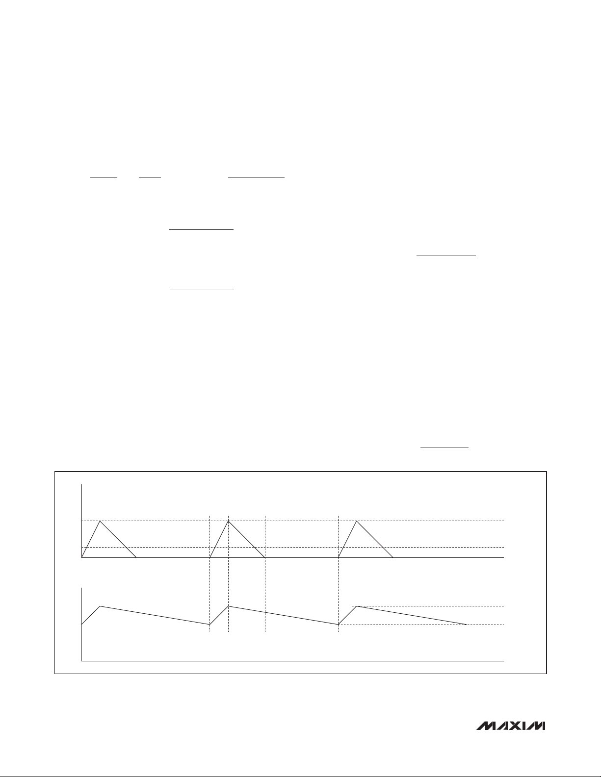
Skip Mode Frequency and Output Ripple
In skip mode, the switching frequency (f
ripple voltage (V
OUT-RIPPLE
) shown in Figure 2 are cal-
) and output
SKIP
culated as follows:
tON is a fixed time (300ns, typ); the peak inductor current
reached is:
V V
−
I t
SKIP LIMIT ON
−
IN OUT
= ×
L
I
L
I
SKIP-LIMIT
t
t
OFF1
ON
V
OUT
Figure 2. Skip Mode Waveform
14 _____________________________________________________________________________________
t
OFF2
= n × tCK
I
LOAD
V
OUT-RIPPLE
Page 15

High-Efficiency, 3A, Current-Mode
( )
Synchronous, Step-Down Switching Regulator
t
is the time needed for inductor current to reach the
OFF1
zero-current crossing limit (~0A):
L I
×
SKIP LIMIT
V
−
OUT
During tON and t
t
=
OFF1
, the output capacitor stores a
OFF1
charge equal to (see Figure 2):
1 1
−
V V V
IN OUT OUT
∆ =
Q
OUT
During t
L x I I x
( )
SKIP LIMIT LOAD
(= n x tCK, number of clock cycles skipped),
OFF2
− +
−
2
2
output capacitor loses this charge:
Q
∆
OUT
= ⇒
I
LOAD
1 1
V V V
−
IN OUT OUT
2 xI
2
LOAD
− +
t
OFF2
t
OFF2
L x I I x
( )
SKIP LIMIT LOAD
−
=
Finally, frequency in skip mode is:
f
SKIP
=
t t t
ON OFF1 OFF2
1
+ +
Output ripple in skip mode is:
V V V
OUT RIPPLE COUT RIPPLE ESR RIPPLE
− − −
R x I I
+ −
V R
OUT RIPPLE ESR,COUT
−
= +
I I x t
( )
SKIP LIMIT LOAD ON
=
ESR,COUT SKIP LIMIT LOAD
= +
C x V V
OUT IN OUT
x I I
( )
SKIP LIMIT LOAD
−
−
C
OUT
( )
−
L x I
SKIP LIMIT
−
−
( )
−
−
the inductor’s pole frequency is shifted beyond the gain
bandwidth of the regulator. System stability is provided
with the addition of a simple series capacitor-resistor from
COMP to GND. This pole-zero combination serves to tailor
the desired response of the closed-loop system. The basic
regulator loop consists of a power modulator (comprising
the regulator’s pulse-width modulator, current sense and
slope compensation ramps, control circuitry, MOSFETs,
and inductor), the capacitive output filter and load, an
output feedback divider, and a voltage-loop error amplifier
with its associated compensation circuitry. See Figure 1.
The average current through the inductor is expressed as:
I G V= ×
L MOD COMP
where IL is the average inductor current and G
power modulator’s transconductance.
For a buck converter:
V R I= ×
OUT LOAD L
where R
is the equivalent load resistor value.
LOAD
Combining the above two relationships, the power modulator’s transfer function in terms of VOUT with respect
to VCOMP is:
V R I
OUT LOAD L
V I
= = ×
COMP L
G
MOD
×
R G
LOAD MOD
The peak current-mode controller’s modulator gain
is attenuated by the equivalent divider ratio of the
load resistance and the current-loop gain’s impedance.
G
becomes:
MOD
G DC g
MOD MC
( )
= ×
R
LOAD
1 K 1 D 0.5
+ × × − −
f L
×
SW
1
( )
S
MOD
MAX15058
is the
To limit output ripple in skip mode, size C
based on
OUT
the above formula. All the above calculations are applicable only in skip mode.
Compensation Design Guidelines
The MAX15058 uses a fixed-frequency, peak-current-mode
control scheme to provide easy compensation and fast
transient response. The inductor peak current is monitored
on a cycle-by-cycle basis and compared to the COMP
voltage (output of the voltage error amplifier). The regulator’s duty cycle is modulated based on the inductor’s peak
current value. This cycle-by-cycle control of the inductor
current emulates a controlled current source. As a result,
______________________________________________________________________________________ 15
where R
LOAD
= V
OUT/IOUT(MAX)
, fSW is the switching
frequency, L is the output inductance, D is the duty cycle
(V
OUT/VIN
), and KS is a slope compensation factor cal-
culated from the following equation:
S V f L g
K 1 1
S
SLOPE SLOPE SW MC
= + = +
S V V
N IN OUT
× × ×
−
( )
where:
V
S V f
SLOPE SLOPE SW
SLOPE
= = ×
t
SW
V V
−
N
IN OUT
=
L g
×
MC
S
Page 16

High-Efficiency, 3A, Current-Mode
( )
Synchronous, Step-Down Switching Regulator
1ST ASYMPTOTE
R2 × (R1 + R2)
GAIN
MAX15058
UNITY
1ST POLE
[2GC
× (10
C
NOTE:
R
OUT
f
PMOD
WHICH FOR
ESR << {R
BECOMES
f
PMOD
f
PMOD
AVEA(dB)/20
= 10
= [2GC
= [2GC
= (2GC
-1)]-1
- g
MV
2ND POLE
f
PMOD
AVEA(dB)/20
× g
× (ESR + {R
OUT
-1
+ [KS × (1 - D) - 0.5] × (L × fSW)-1}
LOAD
× {R
OUT
LOAD
× R
OUT
LOAD
-1
AVEA(dB)/20
× 10
2ND ASYMPTOTE
R2 × (R1 + R2)
*
1ST ZERO
-1
(2GCCRC)
-1
MV
-1
+ [KS × (1 - D) - 0.5] × (L × fSW)-1}-1)]
LOAD
-1
+ [KS × (1 - D) - 0.5] × (L × fSW)-1}-1]
)-1 + [KS × (1 - D) - 0.5] × (2GC
× gMC × R
-1
× gMV × (2GCC)-1 × gMC × R
3RD ASYMPTOTE
R2 × (R1 + R2)
× {R
(2GC
OUT
4TH ASYMPTOTE
R2 × (R1 + R2)
(2GC
f
CO
-1
× {1 + R
LOAD
-1
× gMV × (2GCC)-1 × gMC × R
-1
+ [KS × (1 - D) - 0.5] × (L × fSW)-1}-1)
LOAD
× {R
OUT
3RD POLE (DBL)
0.5 × f
× L × fSW)
OUT
× [KS × (1 - D) - 0.5] × (L × fSW)-1}
LOAD
× {1 + R
LOAD
-1
× gMV × RC × gMC × R
LOAD
SW
-1
LOAD
-1
+ [KS × (1 - D) - 0.5] × (L × fSW)-1}-1)
2ND ZERO
(2GC
OUT
-1
-1
-1
× [KS × (1 - D) - 0.5] × (L × fSW)-1}
× {1 + R
LOAD
-1
ESR)
5TH ASYMPTOTE
R2 × (R1 + R2)-1 × gMV × RC × gMC × R
(2GC
× {R
OUT
6TH ASYMPTOTE
R2 × (R1 + R2)-1 × gMV × RC × gMC × R
ESR × {R
× [KS × (1 - D) - 0.5] × (L × fSW)-1}-1 ×
LOAD
-1
× {1 + R
LOAD
-1
+ [KS × (1 - D) - 0.5] × (L × fSW)-1}-1)-1 × (0.5 × fSW)2 × (2Gf)
LOAD
-1
+ [KS × (1 - D) - 0.5] × (L × fSW)-1}-1 × (0.5 × fSW)2 × (2Gf)
LOAD
× [KS × (1 - D) - 0.5] × (L × fSW)-1}-1 ×
LOAD
-1
-1
LOAD
× {1 + R
LOAD
× [KS × (1 - D) - 0.5] × (L × fSW)-1}-1 ×
LOAD
× {1 + R
× [KS × (1 - D) - 0.5] × (L × fSW)-1}-1 ×
LOAD
FREQUENCY
-2
-2
Figure 3. Asymptotic Loop Response of Current-Mode Regulator
As previously mentioned, the power modulator’s dominant
pole is a function of the parallel effects of the load resistance and the current-loop gain’s equivalent impedance:
f
PMOD
=
π × × + +
2 C ESR
OUT
1
R f L
LOAD SW
K 1 D 0.5
1
× − −
( )
S
×
1
−
And knowing that the ESR is typically much smaller than
the parallel combination of the load and the current loop:
1
( )
×
−
1
−
f
PMOD
1
ESR
<< +
R f L
LOAD SW
≈
π × × +
2 C
OUT
R f L
K 1 D 0.5
× − −
( )
S
×
1
× − −
1
LOAD SW
K 1 D 0.5
S
which can be expressed as:
f
PMOD
≈ +
2 C R 2 f L C
π × × π × × ×
1
OUT LOAD SW OUT
Note: Depending on the application’s specifics, the
amplitude of the slope compensation ramp could have
a significant impact on the modulator’s dominate pole.
For low duty-cycle applications, it provides additional
damping (phase lag) at/near the crossover frequency
(see the Closing the Loop: Designing the Compensation
Circuitry section). There is no equivalent effect on the
power modulator zero, f
f f
= =
ZMOD ZESR
.
ZMOD
2 C ESR
π × ×
OUT
16 _____________________________________________________________________________________
K 1 D 0.5
× − −
S
1
Page 17

High-Efficiency, 3A, Current-Mode
( )
( )
Synchronous, Step-Down Switching Regulator
The effect of the inner current loop at higher frequencies is modeled as a double-pole (complex conjugate)
frequency term, G
G s
SAMPLING
SAMPLING
=
( )
(s), as shown:
2
s s
2
f
π ×
( )
SW
1
+ +
f Q
π × ×
SW C
1
where the sampling effect quality factor, QC, is:
Q
=
C
π × × − −
1
K 1 D 0.5
( )
S
And the resonant frequency is:
ω
SAMPLING
(s) = π × f
SW
or:
f
f
SAMPLING
SW
=
2
Having defined the power modulator’s transfer function,
the total system transfer can be written as follows (see
Figure 3):
Gain(s) = GFF(s) × GEA(s) × G
G
SAMPLING
MOD
(s)
(DC) × G
FILTER
(s) ×
where:
G s
FF
( )
= ×
R1 R2
Leaving CFF empty, G
G s
Also:
AVEA(dB)/20
G s 10
= ×
( )
EA
R2
+
FF(s)
FF
( )
sC R1 1
sC R1||R2 1
FF
becomes:
R2
R1 R2=+
+ +
sC R 1
C C
+
FF
( )
( )
+
sC R 1
+
C C
AVEA(dB)/20
10
g
MV
which simplifies to:
G s 10
when Rg<<
G s R
FILTER LOAD
= ×
( )
EA
C
= ×
( )
AVEA(dB)/20
AVEA(dB)/20
10
MV
sC 1
OUT
R f L
LOAD SW
sC R 1
10
+
sC 1
C
sC ESR 1
( )
OUT
K 1 D 0.5
1
S
+ +
+
C C
AVEA(dB)/20
g
MV
+
× − −
( )
×
1
−
The dominant poles and zeros of the transfer loop gain
are shown below:
g
f
P1
f
=
P2
π × +
2 C
=
π × ×
2 10 C
OUT
R f L
f f
P3 SW
f
Z1
f
=
Z2
MV
AVEA(dB)/20
1
× − −
K 1 D 0.5
1
LOAD SW
1
=
( )
2
=
2 C R
π ×
( )
S
1
C C
1
2 C ESR
π ×
OUT
C
×
The order of pole-zero occurrence is:
f f f f f f< ≤ < ≤ <
P1 P2 Z1 CO P3 Z2
Under heavy load, fP2, approaches fZ1. Figure 3 shows
a graphical representation of the asymptotic system
closed-loop response, including dominant pole and zero
locations.
The loop response’s fourth asymptote (in bold, Figure 3)
is the one of interest in establishing the desired crossover frequency (and determining the compensation
component values). A lower crossover frequency provides for stable closed-loop operation at the expense of
a slower load- and line-transient response. Increasing
the crossover frequency improves the transient response
at the (potential) cost of system instability. A standard
rule of thumb sets the crossover frequency between
1/10 and 1/5 of the switching frequency. First, select
the passive power and decoupling components that
meet the application’s requirements. Then, choose the
small-signal compensation components to achieve the
desired closed-loop frequency response and phase
margin as outlined in the Closing the Loop: Designing
the Compensation Circuitry section.
Closing the Loop: Designing the
Compensation Circuitry
1) Select the desired crossover frequency. Choose fCO
approximately 1/10 to 1/5 of the switching frequency
(fSW).
2) Determine RC by setting the system transfer’s fourth
asymptote gain equal to unity (assuming fCO > fZ1,
fP2, and fP1) where:
MAX15058
−
1
______________________________________________________________________________________ 17
Page 18

High-Efficiency, 3A, Current-Mode
Synchronous, Step-Down Switching Regulator
R K 1 D 0.5
LOAD S
1
+
R1 R2
R 2 f C
= × × π ×
C CO OUT
+
R2 g g R
ESR
MV MC LOAD
+
R L f
LOAD SW
MAX15058
and where the ESR is much smaller than the parallel
combination of the equivalent load resistance and the
current loop impedance, e.g.,:
ESR
<<
R L f
RC becomes:
R1 R2
R
= ×
C
3) Determine CC by selecting the desired first system zero, fZ1, based on the desired phase margin.
Typically, setting fZ1 below 1/5 of fCO provides sufficient phase margin.
f
= ≤
Z1
therefore:
C
C
4) For low duty-cycle applications, the addition of a
phase-leading capacitor (CFF in Figure 1) helps
mitigate the phase lag of the damped half-frequency
double pole. Adding a second zero near to but below
the desired crossover frequency increases both the
closed-loop phase margin and the regulator’s unitygain bandwidth (crossover frequency). Select the
capacitor as follows:
C
=
FF
This guarantees the additional phase-leading zero
occurs at a frequency lower than fCO from:
f
PHASE_LEAD
− −
( )
L f
×
SW
× ×
1
− −
K 1 D 0.5
1
S
+
( )
×
1
K 1 D 0.5
− −
1
LOAD SW
+
R2 g g
2 C R 5
π ×
≥
2 f R
π × ×
( )
S
+
2 f C
π ×
CO OUT
MV MC
1
C C
5
CO C
×
×
f
CO
1
2 f R1|| R2
π × ×
( )
CO
=
1
2 C R1
π × ×
FF
Using CFF the zero-pole order is adjusted as follows:
f f f
< ≤ < < ≈
P1 P2 Z1
1 1
2 C R1 2 C (R1||R2)
π π
FF FF
f f f
< <
CO P3 Z2
Confirm the desired operation of CFF empirically. The
phase lead of CFF diminishes as the output voltage
is a smaller multiple of the reference voltage, e.g.,
below about 1V. Do not use CFF when V
Setting the Soft-Start Time
The soft-start feature ramps up the output voltage slowly,
reducing input inrush current during startup. Size the
CSS capacitor to achieve the desired soft-start time, t
using:
I t
×
SS
SS SS
=
V
FB
C
ISS, the soft-start current, is 10FA (typ) and VFB, the
output feedback voltage threshold, is 0.6V (typ). When
using large C
capacitance values, the high-side
OUT
current limit can trigger during the soft-start period. To
ensure the correct soft-start time, tSS, choose CSS large
enough to satisfy:
V I
×
C C
>> ×
SS OUT
I
is the typical high-side MOSFET current-limit
HSCL_
OUT SS
(I I ) V
− ×
HSCL_ OUT FB
value.
An external tracking reference with steady-state value
between 0V and VIN - 1.8V can be applied to SS/REFIN.
In this case, connect an RC network from external tracking reference and SS/REFIN, as shown in Figure 4. The
recommended value for RSS is approximately 1kI. RSS
is needed to ensure that, during hiccup period, SS/
REFIN can be internally pulled down.
When an external reference is connected to SS/REFIN,
the soft-start must be provided externally.
R
V
REF_EXT
Figure 4. RC Network for External Reference at SS/REFIN
SS
C
SS
SS/REFIN
MAX15058
OUT
= VFB.
SS,
18 _____________________________________________________________________________________
Page 19

High-Efficiency, 3A, Current-Mode
Synchronous, Step-Down Switching Regulator
MAX15058
INPUT
2.8V TO 5.5V
C
22µF
IN
R
PULL
20kI
ON
OFF
C
SS
22nF
IN
MAX15058
PGOOD
ENENABLE
SKIP
SS/REFIN
Figure 5. Application Circuit for PWM Mode Operation
Power Dissipation
The MAX15058 is available in a 9-bump WLP package
and can dissipate up to 1127mW at TA = +70NC. When
the die temperature exceeds +150NC, the thermal-shutdown protection is activated (see the Thermal-Shutdown
Protection section).
Layout Procedure
Careful PCB layout is critical to achieve clean and stable
operation. It is highly recommended to duplicate the
MAX15058 Evaluation Kit layout for optimum performance. If deviation is necessary, follow these guidelines
for good PCB layout:
1) Connect the signal and ground planes at a single point
immediately adjacent to the GND bump of the IC.
L
OUT
GND
COMP
(ICE IN06142)
1µH
LX
1.2I
1nF
FB
R
C
5.36kI
C
C
1nF
C
OUT
22µF x 2
C
100pF
OUTPUT
1.8V AT 3A
FF
R
1
8.06kI
R
2
4.02kI
2) Place capacitors on IN and SS/REFIN as close as
possible to the IC and the corresponding pad using
direct traces.
3) Keep the high-current paths as short and wide as
possible. Keep the path of switching current short
and minimize the loop area formed by LX, the output
capacitors, and the input capacitors.
4) Connect IN, LX, and GND separately to a large copper area to help cool the IC to further improve efficiency.
5) Ensure all feedback connections are short and
direct. Place the feedback resistors and compensation components as close as possible to the IC.
6) Route high-speed switching nodes (such as LX)
away from sensitive analog areas (such as FB and
COMP).
______________________________________________________________________________________ 19
Page 20

High-Efficiency, 3A, Current-Mode
Synchronous, Step-Down Switching Regulator
INPUT
2.8V TO 5.5V
C
22µF
IN
R
PULL
20kI
IN
MAX15058
PGOOD
MAX15058
ON
OFF
C
SS
22nF
Figure 6. Application Circuit for Skip Mode Operation
Chip Information
PROCESS: BiCMOS
ENENABLE
SKIP
SS/REFIN
L
OUT
GND
COMP
(ICE IN06142)
1µH
LX
1.2I
1nF
FB
R
C
5.36kI
C
C
1nF
C
OUT
22µF x 2
C
100pF
OUTPUT
1.8V AT 3A
R
FF
1
8.06kI
R
2
4.02kI
Package Information
For the latest package outline information and land patterns,
go to www.maxim-ic.com/packages. Note that a “+”, “#”, or
“-” in the package code indicates RoHS status only. Package
drawings may show a different suffix character, but the drawing
pertains to the package regardless of RoHS status.
PACKAGE
TYPE
9 WLP W91E1Z+1
PACKAGE
CODE
OUTLINE
NO.
21-0508
20 _____________________________________________________________________________________
LAND
PATTERN NO.
Refer to
Application
Note 1891
Page 21

High-Efficiency, 3A, Current-Mode
Synchronous, Step-Down Switching Regulator
Revision History
MAX15058
REVISION
NUMBER
0 12/10 Initial release —
1 3/11 Revised Package Information section. 20
2 7/11
REVISION
DATE
DESCRIPTION
Changed the 1.65mm x 1.65mm, 9-bump package information to 1.5mm x 1.5mm,
9-bump package information. Inserted Typical Operating Circuit on page one.
PAGES
CHANGED
1, 11
Maxim cannot assume responsibility for use of any circuitry other than circuitry entirely embodied in a Maxim product. No circuit patent licenses are implied.
Maxim reserves the right to change the circuitry and specifications without notice at any time.
Maxim Integrated Products, 120 San Gabriel Drive, Sunnyvale, CA 94086 408-737-7600 21
©
2011 Maxim Integrated Products Maxim is a registered trademark of Maxim Integrated Products, Inc.
 Loading...