

Page 1
19-4747; Rev 0; 9/09
High-Side MOSFET Driver for HB LED Drivers
General Description
The MAX15054 is a high-side, n-channel MOSFET driver
for high-voltage applications capable of switching at high
frequencies. This device is controlled by a CMOS logiclevel signal referenced to ground and features a very
short (12ns, typ) propagation delay from input to output.
The high-voltage operation and high source/sink-current
capability make the MAX15054 ideal for HB LED drivers
and DC-DC converters.
The MAX15054 is well suited to complement other Maxim
LED driver products such as the MAX16814, MAX16838,
MAX16833, MAX16834, and MAX16826. The MAX15054
adds a high-side driver to those products that include only a
low-side driver; it then allows for buck-boost configurations
for multistring drivers similar to the MAX16814, MAX16838,
and MAX16826, and for buck-boost conversion with output
referenced to ground for single-string drivers such as the
MAX16834 and MAX16833.
The MAX15054 is available in the industry-standard 6-pin
SOT23 package and operates over the -40NC to +125NC
automotive temperature range.
and DC-DC Applications
Features
Input Voltage on High-Side n-Channel MOSFET Up
S
to 60V
S Up to 13.5V Logic Input Independent of Supply
Voltage
S 2A Peak Source and Sink Current
S 12ns Propagation Delay
S Rise and Fall Times of 6ns while Driving 1000pF
Capacitance
S Low Input Capacitance
S Low-Side and High-Side Undervoltage Protection
S Allows Buck-Boost Topology Referred to Ground
for LED Drivers and DC-DC Converters
S Allows Buck-Boost Topology for Multistring LED
Drivers
S 6-Pin SOT23 Package
Ordering Information
MAX15054
Applications
HB LED Drivers for Single and Multiple Strings
LED Backlight Drivers
High-Side Driver for DC-DC Converters
(Buck, Buck-Boost, Half-Bridge, Full-Bridge)
PART TEMP RANGE
MAX15054AUT+
-40NC to +125NC
PIN-
PACKAGE
6 SOT23 ACOM
+Denotes a lead(Pb)-free/RoHS-compliant package.
Pin Configuration appears at end of data sheet.
TOP
MARK
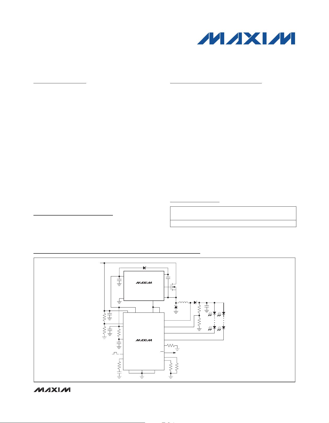
Typical Operating Circuits
V
IN
V
DD
C
1
GND
C
2
R
1
R
2
IN GATE NDRV
EN
V
CC
C
3
R
3
V
DRV
C
4
DIM
COMP
R
4
SGND PGND
C
4
CFB
D
1
MAX15054
MAX16838
HI
LEDGND
HDRV
DRAIN
OUT1
OUT2
BST
C
BST
Q1
LX
OV
R
7
ISET
FLT
CS
RT
R
6
D
3
L1
C
D
2
R
5
5
R
8
R
9
Typical Operating Circuits continued at end of data sheet.
_______________________________________________________________ Maxim Integrated Products 1
For pricing, delivery, and ordering information, please contact Maxim Direct at 1-888-629-4642,
or visit Maxim’s website at www.maxim-ic.com.
Page 2
High-Side MOSFET Driver for HB LED Drivers
and DC-DC Applications
ABSOLUTE MAXIMUM RATINGS
VDD to GND ............................................................. -0.3V to +6V
LX to GND ................................................................-2V to +65V
HDRV to LX ................................................-0.3V to (VDD + 0.3V)
BST to LX ................................................................. -0.3V to +6V
HI to GND .............................................................. -0.3V to +15V
dV/dt at LX ........................................................................50V/ns
Peak Current into HDRV (< 100ns) ...................................... Q2A
Continuous Current into HDRV ..................................... Q100mA
Continuous Power Dissipation (TA = +70NC)
MAX15054
6-Pin SOT23 (derate 8.7mW/NC above +70NC) .........695.7mW
Note 1: Package thermal resistances were obtained using the method described in JEDEC specification JESD51-7, using a four-
layer board. For detailed information on package thermal considerations, refer to www.maxim-ic.com/thermal-tutorial.
Stresses beyond those listed under “Absolute Maximum Ratings” may cause permanent damage to the device. These are stress ratings only, and functional
operation of the device at these or any other conditions beyond those indicated in the operational sections of the specifications is not implied. Exposure to absolute
maximum rating conditions for extended periods may affect device reliability.
ELECTRICAL CHARACTERISTICS
(VDD = V
unless otherwise noted.) (Note 2)
Operating Supply Voltage V
VDD Quiescent Supply Current I
BST Quiescent Supply Current I
BST Operating Supply Current I
VDD Undervoltage Lockout
Threshold
VDD Undervoltage Lockout
Threshold Hysteresis
BST-to-LX Undervoltage
Lockout Threshold
BST-to-LX Undervoltage
Lockout Threshold Hysteresis
LOGIC INPUT (HI)
HI Logic-High Threshold V
HI Logic-Low Threshold V
HI Logic-Input Hysteresis 0.9 V
HI Input Current I
HI Input Resistance R
DRIVER
LX Withstand Voltage V
BST Withstand Voltage V
LX Pulldown Current VLX = 2.5V 500 740 1100
Driver Output Resistance
(Sourcing)
Driver Output Resistance
(Sinking)
= 5V, VLX = V
BST
PARAMETER SYMBOL CONDITIONS MIN TYP MAX UNITS
= 0V, TA = TJ = -40°C to +125°C, unless otherwise noted. Typical values are at TA = TJ = +25°C,
GND
DD
DD
BST
BSTO
V
DD_UVLOVDD
V
BST_
UVLO
IH
IL
IN
IN
LX_MAX
BST_MAX
R
ON_HP
R
ON_HN
No switching 40 75
No switching 65 125
fSW = 500kHz, no load 0.3 1.3 mA
rising 3.92 4.22 4.56 V
BST rising 3.54 3.82 4.1 V
HI = GND -2 +2
V
- VLX = 4.5V,
BST
100mA sourcing
V
- VLX = 4.5V,
BST
100mA sinking
Thermal Resistance (Note 1)
Junction-to-Ambient Thermal Resistance (BJA) .........115NC/W
Junction-to-Case Thermal Resistance (BJC) ................80NC/W
Operating Temperature Range ........................ -40NC to +125NC
Maximum Junction Temperature .....................................+150NC
Storage Temperature Range ............................ -65NC to +150NC
Lead Temperature (soldering, 10s) .................................+300NC
4.6 5.5 V
0.2 V
0.2 V
3.9 V
1.8 V
300
60 V
65 V
TA = +25NC
TA = +125NC
TA = +25NC
TA = +125NC
1 1.5
1.25 2
0.75 1
1 1.5
FA
FA
FA
kI
FA
I
I
2 ______________________________________________________________________________________
Page 3
High-Side MOSFET Driver for HB LED Drivers
and DC-DC Applications
ELECTRICAL CHARACTERISTICS (continued)
(VDD = V
unless otherwise noted.) (Note 2)
Peak Output Current (Sourcing) I
Peak Output Current (Sinking) I
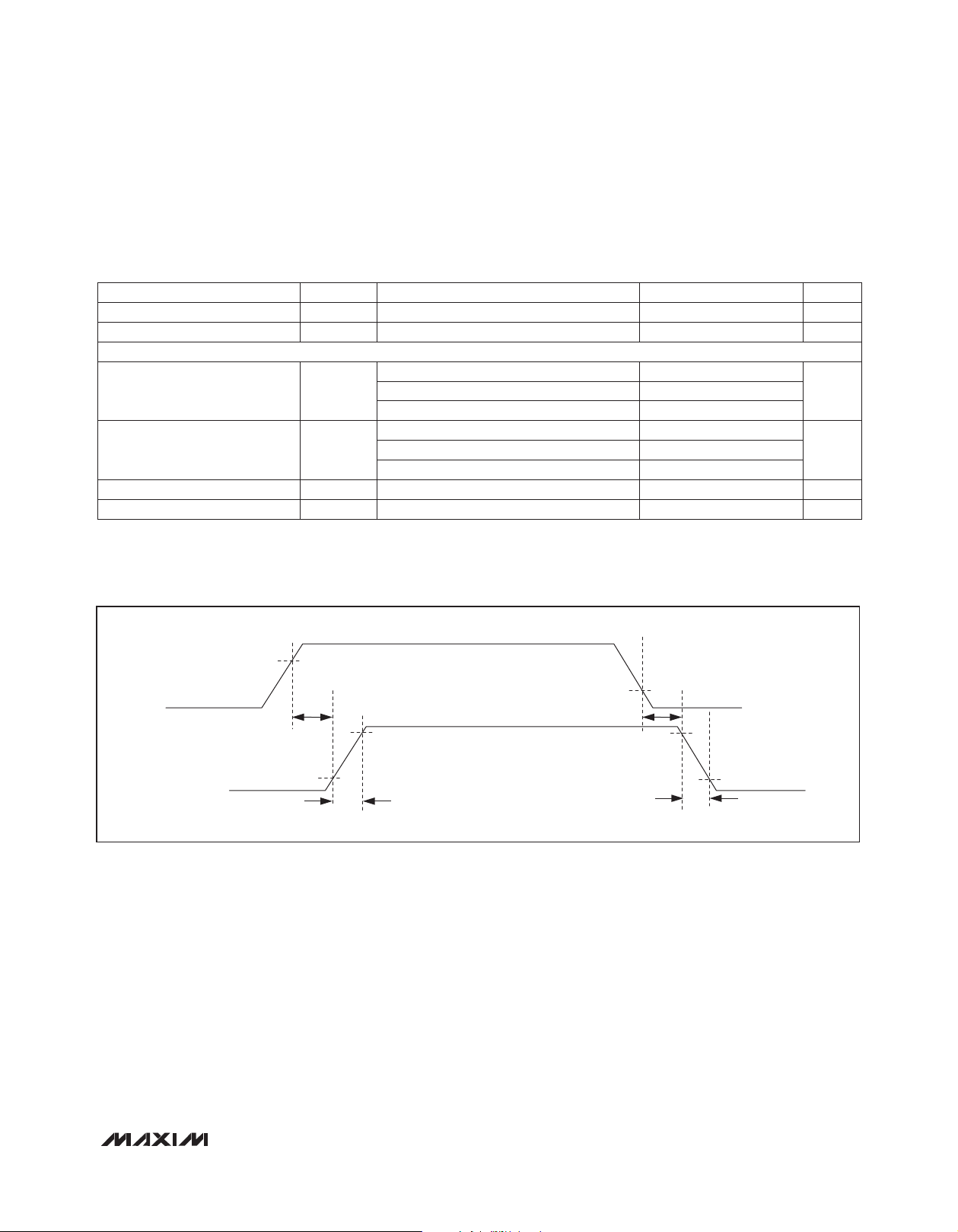
SWITCHING CHARACTERISTICS
Rise Time t
Fall Time t
Turn-On Propagation Delay t
Turn-Off Propagation Delay t
Note 2: All devices are 100% production tested at TA = +25NC. Limits over the operating temperature range are guaranteed by
Note 3: Guaranteed by design.
= 5V, VLX = V
BST
= 0V, TA = TJ = -40°C to +125°C, unless otherwise noted. Typical values are at TA = TJ = +25°C,
GND
PARAMETER SYMBOL CONDITIONS MIN TYP MAX UNITS
V
PK_HP
PK_HN
= 0V 2.5 A
HDRV
V
= 5V 2.5 A
HDRV
No-load capacitor 1.5
R
CL = 5000pF 18
No-load capacitor 1.5
F
CL = 5000pF 16
D_ON
D_OFF
Figure 1, CL = 1000pF (Note 3) 11 25 ns
Figure 1, CL = 1000pF (Note 3) 11 25 ns
design.
nsCL = 1000pF 6
nsCL = 1000pF 6
MAX15054
V
IH
V
HI
t
D_ON
V
HDRV
10%
t
R
Figure 1. Turn-On/Turn-Off Propagation Delay
90%
V
t
D_OFF
IL
t
F
_______________________________________________________________________________________ 3
Page 4

High-Side MOSFET Driver for HB LED Drivers
POWER-UP AND POWER-DOWN SEQUENCE
POWER-UP AND POWER-DOWN SEQUENCE
MAX15054 toc03
0V
HDRV
1V/div
V
DD
1V/div
400µs/div
fSW = 5kHz AT HI
and DC-DC Applications
Typical Operating Characteristics
(VDD = V
= 5V, VLX = V
BST
= 0V, TA = +25°C, unless otherwise noted.)
GND
VDD UNDERVOLTAGE LOCKOUT
THRESHOLD vs. TEMPERATURE
4.250
4.225
4.200
4.175
MAX15054
4.150
4.125
4.100
4.075
UVLO THRESHOLD (V)
4.050
4.025
4.000
3.975
VDD RISING
VDD FALLING
-40 125
TEMPERATURE (NC)
fSW = 5kHz AT HI
1109565 80-10 5 20 35 50-25
40µs/div
3.875
3.850
3.825
MAX15054 toc01
3.800
3.775
3.750
3.725
3.700
UVLO THRESHOLD (V)
3.675
3.650
3.625
3.600
MAX15054 toc04
BST-LX UNDERVOLTAGE LOCKOUT
THRESHOLD vs. TEMPERATURE
BST-LX RISING
BST-LX FALLING
-40 125
TEMPERATURE (°C)
1109565 80-10 5 20 35 50-25
VDD, BST-LX QUIESCENT SUPPLY
70
65
60
V
DD
1V/div
HDRV
1V/div
0V
55
50
45
40
35
30
25
20
QUIESCENT CURRENT (µA)
15
10
5
0
5.5
MAX15054 toc02
CURRENT vs. SUPPLY VOLTAGE
I
BST
TA = +125NC
TA = +85NC
TA = +25NC
I
DD
TA = -40NC
SUPPLY VOLTAGE (V)
MAX15054 toc05
5.04.53.5 4.01.0 1.5 2.0 2.5 3.00.5
2000
1750
1500
1250
(µA)
1000
BSTO
I
750
500
250
0
0.1 10,000
4 ______________________________________________________________________________________
BST OPERATING SUPPLY CURRENT
vs. SWITCHING FREQUENCY
NO LOAD ON HDRV
SWITCHING FREQUENCY (kHz)
10001001.0 10
MAX15054 toc06
HI INPUT THRESHOLDS vs. TEMPERATURE
4.00
3.75
3.50
RISING
3.25
3.00
2.75
INPUT THRESHOLD (V)
2.50
FALLING
2.25
2.00
-40 125
TEMPERATURE (NC)
MAX15054 toc07
11095-25 -10 5 35 50 6520 80
Page 5

High-Side MOSFET Driver for HB LED Drivers
and DC-DC Applications
Typical Operating Characteristics (continued)
(VDD = V
= 5V, VLX = V
BST
= 0V, TA = +25°C, unless otherwise noted.)
GND
MAX15054
2MHz OPERATION
NO LOAD ON HDRV
4% DUTY CYCLE AT 2MHz
10ns/div
200ns/div
MAX15054 toc10
HI
2V/div
0V
HDRV
2V/div
0V
MAX15054 toc08
140
HI
2V/div
0V
HDRV
2V/div
0V
96% DUTY CYCLE AT 2MHz
10ns/div
120
100
80
60
OUTPUT HIGH/LOW (V)
40
20
MAX15054 toc11
HDRV OUTPUT HIGH/LOW
vs. TEMPERATURE
V
BST - VHDRV
SOURCING 100mA
V
HDRV - VLX
SINKING 100mA
OUTPUT HIGH = V
OUTPUT LOW = V
0
-40 125
TEMPERATURE (NC)
BST - VHDRV
HDRV - VLX
1109580655035205-10-25
TURN-ON/TURN-OFF PROPAGATION
DELAY vs. TEMPERATURE
13.0
2V/div
2V/div
12.5
12.0
11.5
11.0
10.5
10.0
9.5
PROPAGATION DELAY (ns)
9.0
8.5
8.0
-40 125
MAX15054 toc09
tD_
OFF
TEMPERATURE (°C)
tD_
MAX15054 toc12
ON
110
9565 80-10 5 20 35 50-25
RISE TIME AND FALL TIME
HI
4.7nF CAPACITOR
CONNECTED FROM
HDRV TO GND,
LX = GND
20ns/div
MAX15054 toc13
2V/div
HDRV
0V
2V/div
HDRV
0V
HI
PROPAGATION DELAY
1nF CAPACITOR CONNECTED
FROM HDRV TO GND,
LX = GND
40ns/div
MAX15054 toc14
HI
HDRV
1V/div
0V
_______________________________________________________________________________________ 5
TURN-ON AND TURN-OFF
Page 6

High-Side MOSFET Driver for HB LED Drivers
and DC-DC Applications
Pin Description
PIN NAME FUNCTION
1 HI
2 GND Ground
3 V
MAX15054
4 BST
5 HDRV High-Side Gate-Driver Output. Driver output to drive the high-side external MOSFET gate.
6 LX Source Connection for High-Side MOSFET. LX also serves as a return terminal for the high-side driver.
DD
Functional Diagram
5V CMOS Logic Input. HI is referenced to GND and is capable of withstanding voltages up to 13.5V for
any VDD voltage.
Input Supply Voltage. Valid supply voltage ranges from 4.6V to 5.5V. Bypass VDD to GND with a 0.1FF
ceramic capacitor as close as possible to the device.
Boost Flying Capacitor Connection. Connect a minimum of a 0.1FF ceramic capacitor between BST
and LX for the high-side MOSFET driver supply. Connect a bootstrap Schottky diode between VDD
and BST.
BST
HIGH-SIDE
UVLO
EXTERNAL
GND
D
1
MAX15054
V
DD
LOW-SIDE
UVLO
HI
Detailed Description
The MAX15054 n-channel MOSFET driver controls an
external high-side MOSFET in high-voltage, high-current
applications. This driver operates with a supply voltage of
4.6V to 5.5V, and consumes only 300FA of supply current
during typical switching operations (fSW = 500kHz) and
no-load conditions. The MAX15054 provides 2.5A (typ)
sink/source peak current and is capable of operating with
large capacitive loads and with switching frequencies
up to 2MHz. The device is used to drive the high-side
MOSFET without requiring an isolation device such as an
optocoupler or a drive transformer.
HDRV
LX
LEVEL
SHIFT UP
LEVEL SHIFT
DOWN
The high-side driver is controlled by a CMOS logic
referenced to ground and is powered by a bootstrap
circuit formed by an external diode and capacitor.
Undervoltage lockout (UVLO) protection is provided for
both the high- and low-side driver supplies (BST and
VDD) and includes a UVLO hysteresis of 0.2V (typ).
The MAX15054’s fast switching times and very short
propagation delays (11ns, typ) are ideal for highfrequency applications. Internal logic circuitry prevents
shoot-through during output state changes and minimizes
package power dissipation.
6 ______________________________________________________________________________________
Page 7

High-Side MOSFET Driver for HB LED Drivers
Undervoltage Lockout
The MAX15054 drives an external high-side MOSFET.
Both the high- and low-side supplies feature separate
UVLO protection that monitors each driver’s input supply
voltage (BST-LX and VDD). The low-side supply UVLO
threshold (V
the driver output low when VDD falls below 4V (typ)
irrespective of the high-side UVLO condition.
The high-side driver UVLO threshold (V
referenced to LX, and pulls HDRV low when V
below 3.6V (typ) with respect to LX. After the MAX15054 is
first energized (VDD > V
(C
BST
does not switch since the BST-to-LX voltage is below
V
BST_UVLO
BST-LX supply through an external Schottky diode and
within a short time C
V
to exceed V
BST
and follows HI. The hysteresis is 0.2V (typ) for both UVLO
thresholds.
The MAX15054 driver contains low on-resistance
p-channel and n-channel devices in a totem pole
configuration for the driver output stage. This allows for
rapid turn-on and turn-off of high gate-charge (Qg)
external switching MOSFETs. The driver exhibits low
drain-to-source resistance (R
lower operating temperatures. Lower R
higher source and sink currents from the device as
the external MOSFET gate capacitance charges and
discharges at a quicker rate, resulting in faster switching
speeds. The peak source and sink current provided by
the driver is 2.5A (typ).
Propagation delay from the logic input (HI) to the driver
output is 12ns (typ) (Figure 1). The internal driver also
contains break-before-make logic to eliminate shootthrough conditions that cause unnecessarily high
operating supply currents, efficiency reduction, and
voltage spikes at VDD.
Voltage from HDRV to LX is approximately equal to VDD
minus the diode drop of the bootstrap diode when in a
high state, and zero when in a low state.
DD_UVLO
) between BST and LX is not charged, and HDRV
. An internal charging circuit charges the
) is referenced to GND and pulls
BST_UVLO
DD_UVLO
charges through VDD and causes
BST
BST_UVLO
), the bootstrap capacitor
. HDRV then starts switching
Output Driver
) that decreases for
DS(ON)
DS(ON)
) is
falls
BST
means
and DC-DC Applications
Bootstrap Diode
Connect an external Schottky diode between VDD and
BST, in conjunction with an external bootstrap capacitor
(C
), to provide the voltage required to turn on the
BST
MOSFET (see the Typical Operating Circuits). The diode
charges the bootstrap capacitor from V
high-side switch is off, and isolates VDD when HDRV is
pulled high when the driver turns on.
Bootstrap Capacitor
The bootstrap capacitor (C
used to ensure adequate charge is available to switch
the high-side MOSFET. This capacitor is charged from
VDD by an external bootstrap diode when the MOSFET
is off. The bootstrap capacitor value should be selected
carefully to avoid oscillations during turn-on and turnoff at the HDRV output. Choose a capacitor value at
least 20 times greater than the total gate capacitance
of the MOSFET being switched. Use a low-ESR ceramic
capacitor (typically a minimum 0.1FF is needed). The
high-side MOSFET’s continuous on-time is limited due
to the charge loss from the high-side driver’s quiescent
current. The maximum on-time is dependent on the size
of C
BST
, I
(125FA, max), and V
BST
) between BST and LX is
BST
BST_UVLO
Driver Logic Input (HI)
The MAX15054 features a 5V CMOS logic input. The
required logic-input levels are independent of VDD and
are capable of withstanding up to 13.5V. For example,
the MAX15054 can be powered by a 5V supply while the
logic inputs are provided from 12V logic. Additionally, HI
is protected against voltage spikes up to 15V, regardless
of the VDD voltage. The logic input has 900mV hysteresis
to avoid double pulsing during signal transition. The logic
input is a high-impedance input (300kI, typ) and should
not be left unconnected to ensure the input logic state is
at a known level. With the logic input unconnected, HDRV
pulls low as VDD rises above the UVLO threshold. The
PWM output from the controller must assume a proper
state while powering up the device.
when the
DD
.
MAX15054
_______________________________________________________________________________________ 7
Page 8

High-Side MOSFET Driver for HB LED Drivers
and DC-DC Applications
Typical Operating Circuits (continued)
V
IN
V
CC
V
DD
C
1
D
1
BST
C
BST
MAX15054
GND
HI
IN
C
2
R
1
MAX15054
NDRV CS
HDRV
LX
Q1
D
L
D
2
R
C
6
9
3
R
C
11
OUT
Q2
C
7
R
12
R
10
EN
C
3
V
CC
R
6
R
7
R
2
C
4
V
CC
R
3
C
5
VDRV
DIM
R
C
C
R
FLAG
5
RSDT
COMP
R
C
RT
8
MAX16814
SGND PGND
OVP
OUT1
OUT4
ISET
LEDGND
R
9
8 ______________________________________________________________________________________
Page 9

High-Side MOSFET Driver for HB LED Drivers
Pin Configuration
TOP VIEW
+
1 6 LX
HI
GND
2
MAX15054
3 4
DD
SOT23
5 HDRV
BSTV
and DC-DC Applications
___Chip Information
PROCESS: BiCMOS
Package Information
For the latest package outline information and land patterns, go
to www.maxim-ic.com/packages.
PACKAGE TYPE PACKAGE CODE DOCUMENT NO.
6 SOT23 U6+1
21-0058
MAX15054
Maxim cannot assume responsibility for use of any circuitry other than circuitry entirely embodied in a Maxim product. No circuit patent licenses are implied.
Maxim reserves the right to change the circuitry and specifications without notice at any time.
Maxim Integrated Products, 120 San Gabriel Drive, Sunnyvale, CA 94086 408-737-7600 9
©
2009 Maxim Integrated Products Maxim is a registered trademark of Maxim Integrated Products, Inc.
 Loading...