

Page 1
General Description
The MAX15041 low-cost, synchronous DC-DC converter with internal switches delivers an output current up to
3A. The MAX15041 operates from an input voltage of
4.5V to 28V and provides an adjustable output voltage
from 0.6V to 90% of V
IN
, set with two external resistors.
The MAX15041 is ideal for distributed power systems,
preregulation, set-top boxes, television, and other consumer applications.
The MAX15041 features a peak-current-mode PWM controller with internally fixed 350kHz switching frequency
and a 90% maximum duty cycle. The current-mode control architecture simplifies compensation design, and
ensures a cycle-by-cycle current limit and fast response
to line and load transients. A high-gain transconductance
error amplifier allows flexibility in setting the external compensation by using a type III compensation scheme,
thereby allowing the use of all ceramic capacitors.
This synchronous buck regulator features internal
MOSFETs that provide better efficiency than asynchronous solutions, while simplifying the design relative to
discrete controller solutions. In addition to simplifying
the design, the integrated MOSFETs minimize EMI,
reduce board space, and provide higher reliability by
minimizing the number of external components.
The MAX15041 also features thermal shutdown and
overcurrent protection (high-side sourcing and low-side
sinking), and an internal 5V LDO with undervoltage
lockout. In addition, this device ensures safe startup
when powering into a prebiased output.
Other features include an externally adjustable soft-start
that gradually ramps up the output voltage and reduces
inrush current. Independent enable control and powergood signals allow for flexible power sequencing.
The MAX15041 is available in a space-saving, highpower, 3mm x 3mm, 16-pin TQFN-EP package and is
fully specified from -40°C to +85°C.
Applications
Distributed Power Systems
Wall Adapters
Preregulators
Set-Top Boxes
Televisions
xDSL Modems
Consumer Products
Features
o Up to 3A of Continuous Output Current
o ±1% Output Accuracy Over Temperature
o 4.5V to 28V Input Voltage Range
o Adjustable Output Voltage Range from 0.606V to
0.9 x V
IN
o Internal 170mΩ R
DS-ON
High-Side and 105mΩ
R
DS-ON
Low-Side Power Switches
o Fixed 350kHz Switching Frequency
o Up to 93% Efficiency
o Cycle-By-Cycle Overcurrent Protection
o Programmable Soft-Start
o Stable with Low-ESR Ceramic Output Capacitors
o Safe Startup into Prebiased Output
o Enable Input and Power-Good Output
o Fully Protected Against Overcurrent and
Overtemperature
o V
DD
LDO Undervoltage Lockout
o Space-Saving, Thermally Enhanced, 3mm x 3mm
Package
MAX15041
Low-Cost, 3A, 4.5V to 28V Input, 350kHz, PWM
Step-Down DC-DC Regulator with Internal Switches
________________________________________________________________
Maxim Integrated Products
1
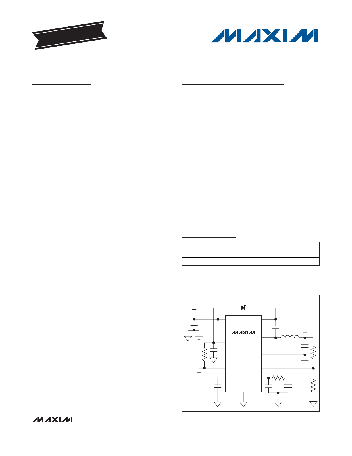
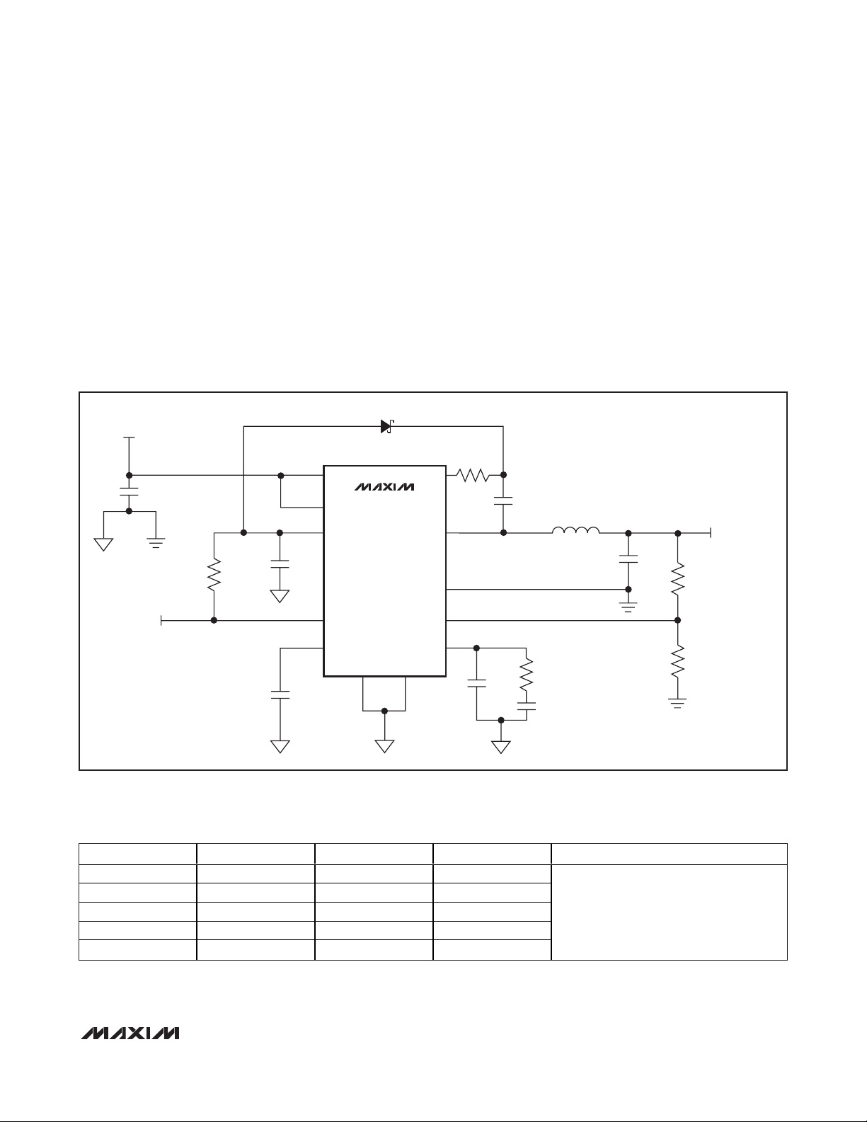
Typical Operating Circuit
Ordering Information
19-4815; Rev 0; 7/09
For pricing, delivery, and ordering information, please contact Maxim Direct at 1-888-629-4642,
or visit Maxim’s website at www.maxim-ic.com.
EVALUATION KIT
AVAILABLE
PART
TEMP RANGE
PIN-
TOP
MARK
MAX15041ETE+
AGV
+
Denotes a lead(Pb)-free/RoHS-compliant package.
*
EP = Exposed pad.
Pin Configuration appears at end of data sheet.
PACKAGE
-40°C to +85°C 16 TQFN-EP*
INPUT
12V
PGOOD
IN
EN
V
DD
PGOOD
SS
MAX15041
SGND
BST
PGND
COMP
OUTPUT
1.8V AT 3A
LX
FB
Page 2
MAX15041
Low-Cost, 3A, 4.5V to 28V Input, 350kHz, PWM
Step-Down DC-DC Regulator with Internal Switches
2 _______________________________________________________________________________________
ABSOLUTE MAXIMUM RATINGS
ELECTRICAL CHARACTERISTICS
(VIN= 12V, C
VDD
= 1µF, CIN= 22µF, TA= TJ= -40°C to +85°C, typical values are at TA= +25°C, unless otherwise noted.) (Note 3)
Stresses beyond those listed under “Absolute Maximum Ratings” may cause permanent damage to the device. These are stress ratings only, and functional
operation of the device at these or any other conditions beyond those indicated in the operational sections of the specifications is not implied. Exposure to
absolute maximum rating conditions for extended periods may affect device reliability.
Note 1: LX has internal clamp diodes to PGND and IN. Applications that forward bias these diodes should take care not to exceed
the IC’s package power dissipation.
Note 2: Package thermal resistances were obtained using the method described in JEDEC specification JESD51-7, using a four-
layer board. For detailed information on package thermal considerations, refer to www.maxim-ic.com/thermal-tutorial
.
IN to SGND.............................................................-0.3V to +30V
EN to SGND.................................................-0.3V to (V
IN
+ 0.3V)
LX to PGND ................................-0.3V to min (+30V, V
IN
+ 0.3V)
LX to PGND .....................-1V to min (+30V, V
IN
+ 0.3V) for 50ns
PGOOD to SGND .....................................................-0.3V to +6V
V
DD
to SGND............................................................-0.3V to +6V
COMP, FB, SS to SGND..............-0.3V to min (+6V, V
DD
+ 0.3V)
BST to LX .................................................................-0.3V to +6V
BST to SGND .........................................................-0.3V to +36V
SGND to PGND ....................................................-0.3V to +0.3V
LX Current (Note 1) ....................................................-5A to +8A
Converter Output Short-Circuit Duration ...................Continuous
Continuous Power Dissipation (T
A
= +70°C)
16-Pin TQFN-EP (derate 14.7mW/°C above +70°C)
Multilayer Board .........................................................1666mW
Package Thermal Resistance (Note 2)
θ
JA
................................................................................48°C/W
θ
JC
..................................................................................7°C/W
Operating Temperature Range ..........................-40°C to +85°C
Junction Temperature .....................................................+150°C
Storage Temperature Range ............................-65°C to +150°C
Lead Temperature (soldering, 10s) .................................+300°C
STEP-DOWN CONVERTER
Input-Voltage Range V
Input Supply Current I
Shutdown Input Supply Current
ENABLE INPUT
EN Shutdown Threshold Voltage V
EN Shutdown Voltage Hysteresis V
EN Lockout Threshold Voltage
EN Input Current I
POWER-GOOD OUTPUT
PGOOD Threshold V
PGOOD Threshold Hysteresis V
PGOOD Output Low Voltage V
PGOOD Leakage Current I
ERROR AMPLIFIER
Error Amplifier
Transconductance
Error Amplifier Voltage Gain A
FB Set-Point Accuracy V
FB Input Bias Current I
PARAMETER SYMBOL CONDITIONS MIN TYP MAX UNITS
IN
IN
EN_SHDN
EN_HYST
V
EN_LOCK
V
EN_LOCK_HYSTVEN
EN
PGOOD_THVFB
PGOOD_HYST
PGOOD_OLIPGOOD
PGOOD
g
MV
VEA
FB
FB
Switching 2.1 4 mA
VEN = 0V, V
V
= 0V, VIN = V
EN
VEN rising 1.4 V
VEN rising 1.7 1.95 2.15 V
falling 100 mV
VEN = 2.9V 2 5.3 9 µA
rising 540 560 584 mV
V
PGOOD
VFB = 0.5V -100 +100
VFB = 0.7V -100 +100
regulated by internal
DD
= 5V 18 28
DD
= 5mA, VFB = 0.5V 35 100 mV
= 5V, VFB = 0.7V 10 nA
4.5 28 V
212
100 mV
15 mV
1.6 mS
90 dB
600 606 612 mV
µA
nA
Page 3
MAX15041
Low-Cost, 3A, 4.5V to 28V Input, 350kHz, PWM
Step-Down DC-DC Regulator with Internal Switches
_______________________________________________________________________________________ 3
Note 3: Specifications are 100% production tested at TA= +25°C. Limits over the operating temperature range are guaranteed by
design and characterization.
ELECTRICAL CHARACTERISTICS (continued)
(VIN= 12V, C
VDD
= 1µF, CIN= 22µF, TA= TJ= -40°C to +85°C, typical values are at TA= +25°C, unless otherwise noted.) (Note 3)
SS Current I
SS Discharge Resistance R
SS Prebiased Mode Stop Voltage 0.65 V
Current Sense to COMP
Transconductance
COMP Clamp Low VFB = 0.7V 0.68 V
PWM Compensation Ramp Valley 830 mV
PWM CLOCK
Switching Frequency f
Maximum Duty Cycle D 90 %
Minimum Controllable On-Time 150 ns
INTERNAL LDO OUTPUT (VDD)
VDD Output Voltage V
VDD Short-Circuit Current VIN = 6.5V 30 80 mA
LDO Dropout Voltage I
V
Undervoltage Lockout
DD
Threshold
V
Undervoltage Lockout
DD
Hysteresis
POWER SWITCH
LX On-Resistance
High-Side Switch Source
Current-Limit Threshold
Low-Side Switch Sink
Current-Limit Threshold
LX Leakage Current
BST Leakage Current V
THERMAL SHUTDOWN
Thermal-Shutdown Threshold Rising +155 °C
Thermal-Shutdown Hysteresis 20 °C
HICCUP PROTECTION
Blanking Time
PARAMETER SYMBOL CONDITIONS MIN TYP MAX UNITS
SS
SS
G
MOD
SW
DD
V
UVLO_TH
V
UVLO_HYST
VSS = 0.45V, sourcing 4.5 5 5.5 µA
ISS = 10mA, sinking, VEN = 1.6V 6 Ω
9S
315 350 385 kHz
I
= 1mA to 25mA, VIN = 6.5V 4.75 5.1 5.5 V
VDD
= 25mA, VDD drops by -2% 50 600 mV
VDD
V
rising 4 4.25 V
DD
150 mV
High-side switch, ILX = 1A 170 305
Low-side switch, I
V
= 33V, VIN = V
BST
= 5V, VIN = 28V, V
V
BST
= 33V, VIN = VLX = 28V 10 nA
BST
= 1A 105 175
LX
5 6 7.2 A
-3 A
= 28V 10
LX
= 0V 10
LX
16 x Soft-
Start Time
mΩ
nA
Page 4
MAX15041
Low-Cost, 3A, 4.5V to 28V Input, 350kHz, PWM
Step-Down DC-DC Regulator with Internal Switches
4 _______________________________________________________________________________________
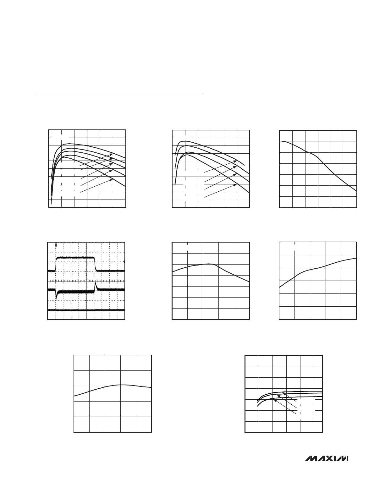
Typical Operating Characteristics
(VIN= 12V, V
OUT
= 3.3V, C
VDD
= 1µF, CIN= 22µF, TA= +25°C, circuit of Figure 3 (see Table 1 for values), unless otherwise specified.)
EFFICIENCY vs. LOAD CURRENT
100
VIN = 12V
95
90
85
80
75
70
EFFICIENCY (%)
65
60
55
50
V
= 5.0V
OUT
V
= 3.3V
OUT
V
= 2.5V
OUT
V
= 1.8V
OUT
V
= 1.2V
OUT
0 3.0
LOAD CURRENT (A)
LOAD-TRANSIENT WAVEFORMS
200µs/div
2.52.01.51.00.5
MAX15041 toc04
MAX15041 toc01
I
LOAD
2A/div
V
OUT
AC-COUPLED
200mV/div
V
PGOOD
5V/div
EFFICIENCY vs. LOAD CURRENT
100
VIN = 5V
95
90
85
80
75
70
EFFICIENCY (%)
65
60
55
50
V
= 3.3V
OUT
V
= 2.5V
OUT
V
= 1.8V
OUT
V
= 1.2V
OUT
0 3.0
LOAD CURRENT (A)
NORMALIZED OUTPUT VOLTAGE
vs. TEMPERATURE
1.002
I
= 0A
LOAD
1.001
1.000
0.999
0.998
0.997
NORMALIZED OUTPUT VOLTAGE
0.996
0.995
-40 85
TEMPERATURE (NC)
OUTPUT-VOLTAGE REGULATION
vs. LOAD CURRENT
0.2
MAX15041 toc02
2.52.01.51.00.5
0
-0.2
-0.4
-0.6
-0.8
OUTPUT-VOLTAGE REGULATION (%)
-1.0
-1.2
03.0
LOAD CURRENT (A)
MAX15041 toc03
2.52.01.51.00.5
NORMALIZED OUTPUT VOLTAGE
vs. TEMPERATURE
1.004
I
= 2A
LOAD
1.002
MAX15041 toc05
1.000
0.998
0.996
NORMALIZED OUTPUT VOLTAGE
0.994
0.992
603510-15
-40 85
TEMPERATURE (NC)
603510-15
MAX15041 toc06
FB SET POINT vs.TEMPERATURE
610
608
606
604
FB SET POINT (mV)
602
600
-40 85
TEMPERATURE (NC)
385
MAX15041 toc07
603510-15
375
365
355
345
FREQUENCY (kHz)
335
325
315
vs. INPUT VOLTAGE
INPUT VOLTAGE (V)
SWITCHING FREQUENCY
MAX15041 toc08
TA = +85NC
TA = +25NC
TA = -40NC
2520151050
Page 5
MAX15041
Low-Cost, 3A, 4.5V to 28V Input, 350kHz, PWM
Step-Down DC-DC Regulator with Internal Switches
_______________________________________________________________________________________
5
Typical Operating Characteristics (continued)
(VIN= 12V, V
OUT
= 3.3V, C
VDD
= 1µF, CIN= 22µF, TA= +25°C, circuit of Figure 3 (see Table 1 for values), unless otherwise specified.)
INPUT SUPPLY CURRENT (mA)
16
L = 4.7FH
I
LOAD
15
14
13
12
11
10
0
INPUT SUPPLY CURRENT
vs. INPUT VOLTAGE
= 0A
INPUT VOLTAGE (V)
SHUTDOWN WAVEFORMS
252015105
MAX15041 toc12
SHUTDOWN CURRENT
vs. TEMPERATURE
TEMPERATURE (NC)
MAX15041 toc13
V
2V/div
I
IN
5A/div
I
L
5A/div
V
2V/div
MAX15041 toc09
V
EN
5V/div
V
OUT
2V/div
I
L
2A/div
V
PGOOD
5V/div
SHUTDOWN CURRENT
vs. INPUT VOLTAGE
MAX15041 toc10
4.0
3.5
3.0
2.5
2.0
SHUTDOWN CURRENT (FA)
1.5
1.0
-40 85
10
9
8
7
6
5
4
3
SHUTDOWN CURRENT (FA)
2
1
0
INPUT VOLTAGE (V)
2520151050
OUTPUT SHORT-CIRCUIT WAVEFORMS
MAX15041 toc11
603510-15
OUT
SS
100µs/div
SWITCHING WAVEFORMS
1µs/div
MAX15041 toc14
V
LX
10V/div
I
L
2A/div
V
OUT
AC-COUPLED
50mV/div
SOFT-START WAVEFORMS
10µs/div
400µs/div
MAX15041 toc15
V
EN
5V/div
V
OUT
2V/div
I
L
2A/div
V
PGOOD
5V/div
Page 6
MAX15041
Low-Cost, 3A, 4.5V to 28V Input, 350kHz, PWM
Step-Down DC-DC Regulator with Internal Switches
6 _______________________________________________________________________________________
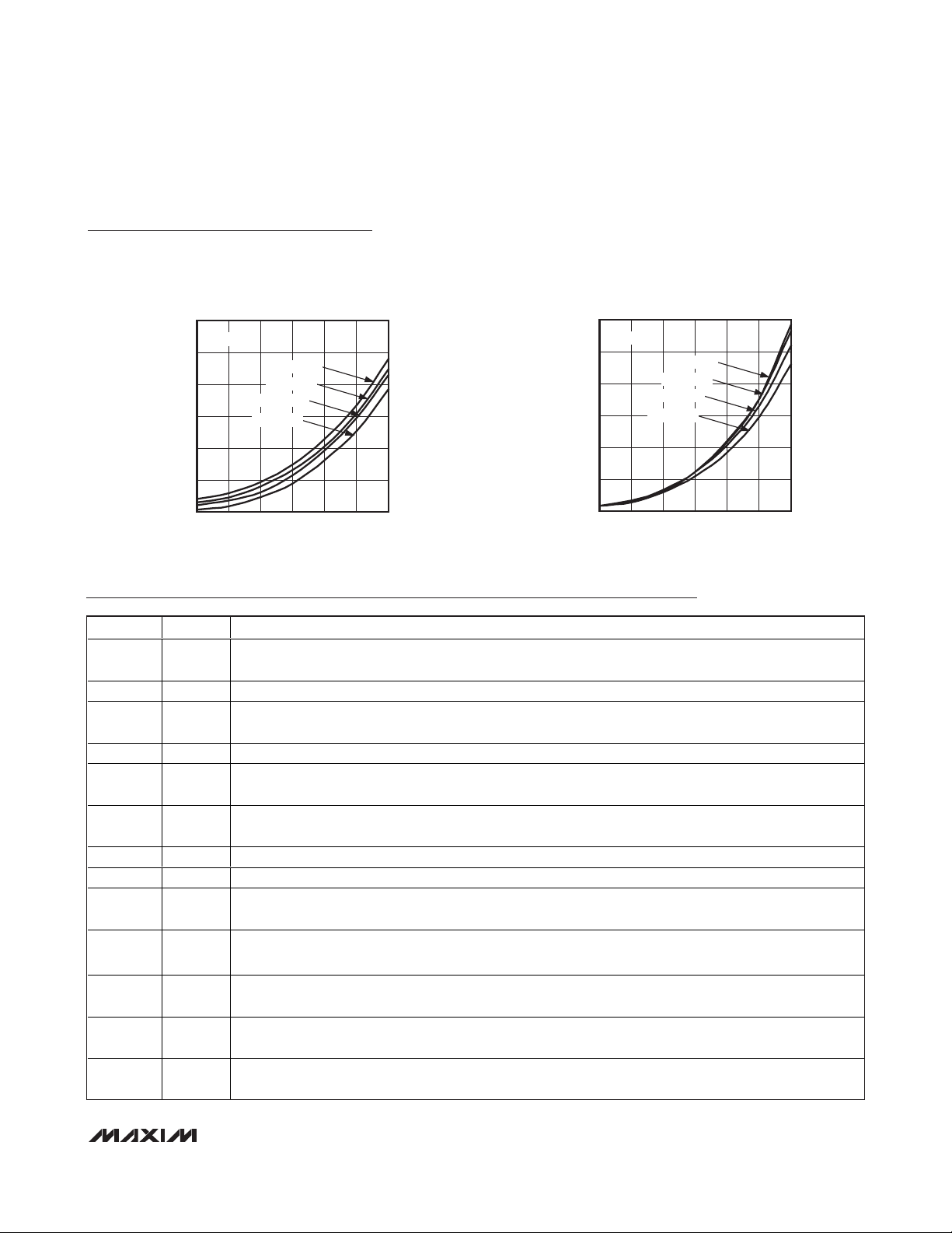
Typical Operating Characteristics (continued)
(VIN= 12V, V
OUT
= 3.3V, C
VDD
= 1µF, CIN= 22µF, TA= +25°C, circuit of Figure 3 (see Table 1 for values), unless otherwise specified.)
1000
100
10
SOFT-START TIME (ms)
1
0.1
1 1000
STARTUP INTO PREBIASED OUTPUT
SOFT-START TIME
vs. CAPACITANCE
10010
CSS (nF)
400µs/div
MAX15041 toc18
MAX15041 toc16
V
EN
5V/div
V
OUT
2V/div
I
L
5A/div
I
OUT
5A/div
STARTUP INTO PREBIASED OUTPUT
400µs/div
MAX15041 toc17
V
EN
5V/div
V
OUT
2V/div
I
L
2A/div
I
OUT
2A/div
MAXIMUM LOAD CURRENT
vs. AMBIENT TEMPERATURE
3.2
VIN = 5V
TJ P +150NC
3.0
2.8
V
= 3.3V
2.6
2.4
MAXIMUM LOAD CURRENT (A)
2.2
2.0
OUT
V
= 2.5V
OUT
V
= 1.8V
OUT
V
= 1.2V
OUT
585
AMBIENT TEMPERATURE (NC)
MAX15041 toc19
75655545352515
MAXIMUM LOAD CURRENT
vs. AMBIENT TEMPERATURE
3.2
VIN = 12V
TJ P +150NC
3.0
2.8
V
= 3.3V
OUT
V
2.6
2.4
MAXIMUM LOAD CURRENT (A)
2.2
2.0
= 2.5V
OUT
V
= 1.8V
OUT
V
= 1.2V
OUT
585
AMBIENT TEMPERATURE (NC)
MAX15041 toc20
75655545352515
3.2
3.0
2.8
2.6
2.4
MAXIMUM LOAD CURRENT (A)
2.2
2.0
MAXIMUM LOAD CURRENT
vs. AMBIENT TEMPERATURE
VIN = 28V
TJ P +150NC
V
= 1.2V
OUT
V
= 3.3V
OUT
V
= 2.5V
OUT
V
= 1.8V
OUT
585
AMBIENT TEMPERATURE (NC)
MAX15041 toc21
75655545352515
Page 7
MAX15041
Low-Cost, 3A, 4.5V to 28V Input, 350kHz, PWM
Step-Down DC-DC Regulator with Internal Switches
_______________________________________________________________________________________ 7
Pin Description
Typical Operating Characteristics (continued)
(VIN= 12V, V
OUT
= 3.3V, C
VDD
= 1µF, CIN= 22µF, TA= +25°C, circuit of Figure 3 (see Table 1 for values), unless otherwise specified.)
DEVICE POWER DISSIPATION
vs. LOAD CURRENT
3.0
VIN = 12V
2.5
2.0
1.5
1.0
POWER DISSIPATION (W)
0.5
0
0 3.0
V
= 3.3V
OUT
V
= 2.5V
OUT
V
= 1.8V
OUT
V
= 1.2V
OUT
LOAD CURRENT (A)
DEVICE POWER DISSIPATION
vs. LOAD CURRENT
3.0
VIN = 5V
MAX15041 toc22
2.52.01.51.00.5
2.5
2.0
1.5
1.0
POWER DISSIPATION (W)
0.5
0
03.0
V
= 3.3V
OUT
V
= 2.5V
OUT
V
= 1.8V
OUT
V
= 1.2V
OUT
LOAD CURRENT (A)
PIN NAME FUNCTION
1V
2 PGOOD Power-Good Open-Drain Output. PGOOD goes low if FB is below 545mV.
3EN
4 COMP Voltage Error-Amplifier Output. Connect the necessary compensation network from COMP to SGND.
5FB
6SS
7 SGND Analog Ground. Connect to PGND plane at one point near the input bypass capacitor return terminal.
8 I.C. Internally Connected. Connect to SGND.
9 BST
10, 11, 12 LX
13, 14 PGND
15, 16 IN
—EP
Internal LDO 5V Output. Supply input for the internal analog core. Bypass with a ceramic capacitor of at
DD
least 1µF to SGND. See Figure 3.
Enable Input. EN is a digital input that turns the regulator on and off. Drive EN high to turn on the regulator.
Connect to IN for always-on operations.
Feedback Input. Connect FB to the center tap of an external resistor-divider from the output to SGND to set
the output voltage from 0.606V to 90% of V
.
IN
Soft-Start Input. Connect a capacitor from SS to SGND to set the soft-start time (see the Setting the Soft-
Start Time section).
High-Side MOSFET Driver Supply. Bypass BST to LX with a 10nF capacitor. Connect an external diode
(see the Diode Selection section) from V
to BST.
DD
Inductor Connection. Connect the LX pin to the switched side of the inductor. LX is high impedance when
the IC is in shutdown mode, thermal shutdown mode, or V
is below the UVLO threshold.
DD
Power Ground. Connect to the SGND PCB copper plane at one point near the input bypass capacitor
return terminal.
Input Power Supply. Input supply range is from 4.5V to 28V. Bypass with a ceramic capacitor of at least
22µF to PGND.
Exposed Pad. Connect to SGND externally. Solder the exposed pad to a large contiguous copper plane to
maximize thermal performance.
MAX15041 toc23
2.52.01.51.00.5
Page 8
MAX15041
Low-Cost, 3A, 4.5V to 28V Input, 350kHz, PWM
Step-Down DC-DC Regulator with Internal Switches
8 _______________________________________________________________________________________
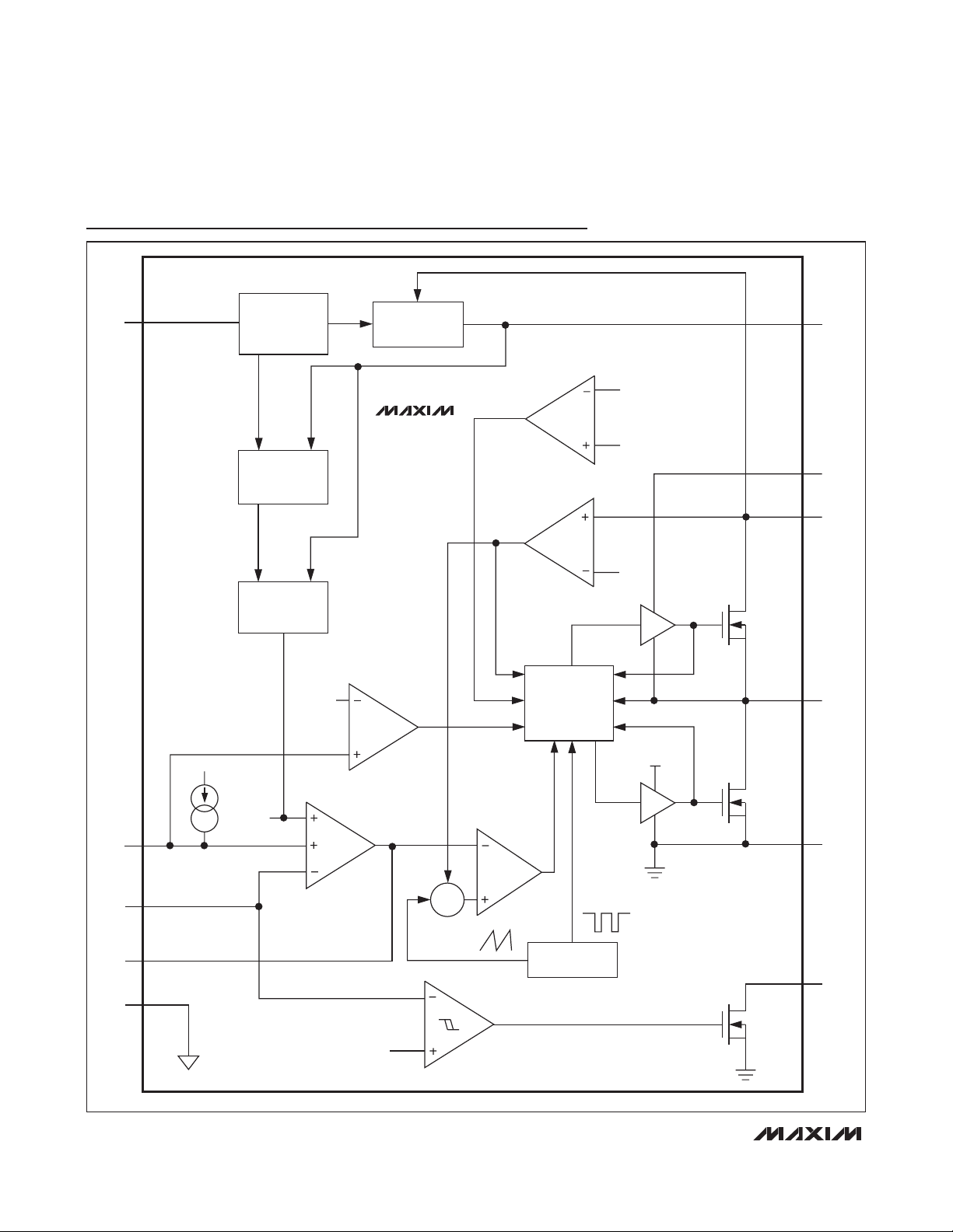
Simplified Block Diagram
EN
5µA
SSFBSS
ENABLE CONTROL
AND THERMAL
SHUTDOWN
BIAS
GENERATOR
VOLTAGE
REFERENCE
0.606V
0.65V
5V LDO
MAX15041
STRONG PREBIAS
COMPARATOR
CURRENT-SENSE/CURRENT-LIMIT
PWM
COMPARATOR
UVLO
COMPARATOR
AMPLIFIER
CONTROL
LOGIC AND
SINK LIMIT
V
DD
4V
V
DD
BST
IN
LX
N
LX
V
DD
N
PGND
ERROR
AMPLIFIER
COMP
SGND
0.560V RISING,
0.545V FALLING
Σ
OSCILLATOR
POWER-GOOD
COMPARATOR
PGOOD
N
Page 9

MAX15041
Low-Cost, 3A, 4.5V to 28V Input, 350kHz, PWM
Step-Down DC-DC Regulator with Internal Switches
_______________________________________________________________________________________ 9
Detailed Description
The MAX15041 is a high-efficiency, peak-currentmode, step-down DC-DC converter with integrated
high-side (170mΩ, typ) and low-side (105mΩ, typ)
power switches. The output voltage is set from 0.606V
to 0.9 x VINby using an adjustable, external resistive
divider and can deliver up to 3A load current. The 4.5V
to 28V input voltage range makes the device ideal for
distributed power systems, notebook computers, and
preregulation applications.
The MAX15041 features a PWM, internally fixed 350kHz
switching frequency with a 90% maximum duty cycle.
PWM current-mode control allows for an all-ceramic
capacitor solution. The MAX15041 comes with a highgain transconductance error amplifier. The currentmode control architecture simplifies compensation
design and ensures a cycle-by-cycle current limit and
fast reaction to line and load transients. The low
R
DS-ON
, on-chip, MOSFET switches ensure high efficiency at heavy loads and minimize critical inductances, reducing layout sensitivity.
The MAX15041 also features thermal shutdown and
overcurrent protection (high-side sourcing and low-side
sinking), and an internal 5V, LDO with undervoltage
lockout. An externally adjustable voltage soft-start
gradually ramps up the output voltage and reduces
inrush current. Independent enable control and powergood signals allow for flexible power sequencing. The
MAX15041 also provides the ability to start up into a
prebiased output, below or above the set point.
Controller Function–PWM Logic
The MAX15041 operates at a constant 350kHz switching frequency. When EN is high, after a brief settling
time, PWM operation starts when VSScrosses the FB
voltage, at the beginning of soft-start.
The first operation is always a high-side MOSFET turnon, at the beginning of the clock cycle. The high-side
MOSFET is turned off when:
1) COMP voltage crosses the internal current-mode
ramp waveform, which is the sum of the compensation ramp and the current-mode ramp derived from
the inductor current waveform (current-sense block).
2) The high-side MOSFET current limit is reached.
3) The maximum duty cycle of 90% is reached.
Then, the low-side MOSFET turns on; the low-side
MOSFET turns off when the clock period ends.
Starting into a Prebiased Output
The MAX15041 is capable of safely soft-starting into a
prebiased output without discharging the output
capacitor. Starting up into a prebiased condition, both
low-side and high-side MOSFETs remain off to avoid
discharging the prebiased output. PWM operation
starts only when the SS voltage crosses the FB voltage.
The MAX15041 is also capable of soft-starting into an
output prebiased above the OUT nominal set point. In
this case, forced PWM operation starts when SS voltage reaches 0.65V (typ).
In case of a prebiased output, below or above the OUT
nominal set point, if the low-side MOSFET sink current
reaches the sink current limit (-3A, typ), the low-side
MOSFET turns off before the end of the clock period
and the high-side MOSFET turns on until one of the following conditions happens:
1) High-side MOSFET source current hits the reduced
high-side MOSFET current limit (0.75A, typ); in this
case, the high-side MOSFET is turned off for the
remaining clock period.
2) The clock period ends.
Enable Input and Power-Good Output
The MAX15041 features independent device enable
control and power-good signals that allow for flexible
power sequencing. The enable input (EN) is an input
with a 1.95V (typ) threshold that controls the regulator.
Assert a voltage exceeding the threshold on EN to
enable the regulator, or connect EN to IN for always-on
operations. Power-good (PGOOD) is an open-drain
output that deasserts (goes high impedance) when V
FB
is above 560mV (typ), and asserts low if VFBis below
545mV (typ).
When the EN voltage is higher than 1.4V (typ) and
lower than 1.95V (typ), most of the internal blocks are
disabled, only an internal coarse preregulator, including the EN accurate comparator, is kept on.
Page 10

MAX15041
Low-Cost, 3A, 4.5V to 28V Input, 350kHz, PWM
Step-Down DC-DC Regulator with Internal Switches
10 ______________________________________________________________________________________
Programmable Soft-Start (SS)
The MAX15041 utilizes a soft-start feature to slowly ramp
up the regulated output voltage to reduce input inrush
current during startup. Connect a capacitor from SS to
SGND to set the startup time (see the
Setting the Soft-
Start Time
section for capacitor selection details).
Internal LDO (VDD)
The MAX15041 has an internal 5.1V (typ) LDO. VDDis
externally compensated with a minimum 1µF, low-ESR
ceramic capacitor. The VDDvoltage is used to supply
the low-side MOSFET driver, and to supply the internal
control logic. When the input supply (IN) is below 4.5V,
VDDis 50mV (typ) lower than IN. The VDDoutput current limit is 80mA (typ) and an UVLO circuit inhibits
switching when V
DD
falls below 3.85V (typ).
Error Amplifier
A high-gain error amplifier provides accuracy for the voltage feedback loop regulation. Connect the necessary
compensation network between COMP and SGND (see
the
Compensation Design Guidelines
section). The erroramplifier transconductance is 1.6mS (typ). COMP clamp
low is set to 0.68V (typ), just below the PWM ramp compensation valley, helping COMP to rapidly return to correct set point during load and line transients.
PWM Comparator
The PWM comparator compares COMP voltage to the
current-derived ramp waveform (LX current to COMP voltage transconductance value is 9A/V, typ.). To avoid instability due to subharmonic oscillations when the duty cycle
is around 50% or higher, a compensation ramp is added
to the current-derived ramp waveform. The compensation
ramp slope (0.45V x 350kHz) is equivalent to half of the
inductor current down slope in the worst case (load 3A,
current ripple 30% and maximum duty cycle operation of
90%). Compensation ramp valley is set at 0.83V (typ).
Overcurrent Protection
and Hiccup Mode
When the converter output is shorted or the device is
overloaded, the high-side MOSFET current-limit event
(6A, typ) turns off the high-side MOSFET and turns on
the low-side MOSFET. In addition, it discharges the SS
capacitor, CSSfor a fixed period of time (∆T0= 70ns,
typ). If the overcurrent condition persists, SS is pulled
below 0.606V and a hiccup event is triggered.
During a hiccup event, high-side and low-side
MOSFETs are kept off, and COMP is pulled low for a
period equal to 16 times the nominal soft-start time
(blanking time). This is obtained by charging SS from 0
to 0.606V with a 5µA (typ) current, and then slowly discharging it back to 0V with a 333nA (typ) current. After
the blanking time has elapsed, the device attempts to
restart. If the overcurrent fault has cleared, the device
resumes normal operation, otherwise a new hiccup
event is triggered (see the Output Short-Circuit
Waveforms in the
Typical Operating Characteristics
).
Thermal-Shutdown Protection
The MAX15041 contains an internal thermal sensor that
limits the total power dissipation in the device and protects it in the event of an extended thermal fault condition. When the die temperature exceeds +155°C (typ),
the thermal sensor shuts down the device, turning off
the DC-DC converter and the LDO regulator to allow
the die to cool. After the die temperature falls by 20°C
(typ), the device restarts, using the soft-start sequence.
Applications Information
Setting the Output Voltage
Connect a resistive divider (R1and R2, see Figures 1
and 2) from OUT to FB to SGND to set the DC-DC converter output voltage. Choose R1and R2so that the DC
errors due to the FB input bias current do not affect the
output-voltage precision. With lower value resistors, the
DC error is reduced, but the amount of power consumed
in the resistive divider increases. A typical tradeoff value
for R2is 10kΩ, but values between 5kΩ and 50kΩ are
acceptable. Once R2is chosen, calculate R1using:
where the feedback threshold voltage V
FB
= 0.606V
(typ).
⎛
V
RR
12
OUT
⎜
V
⎝
FB
⎞
1=× −
⎟
⎠
Page 11

Inductor Selection
A larger inductor value results in reduced inductor ripple
current, leading to a reduced output ripple voltage.
However, a larger inductor value results in either a larger
physical size or a higher series resistance (DCR) and a
lower saturation current rating. Typically, inductor value
is chosen to have current ripple equal to 30% of load
current. Choose the inductor with the following formula:
where f
SW
is the internally fixed 350kHz switching fre-
quency, and ∆I
L
is the estimated inductor ripple current
(typically set to 0.3 x I
LOAD
). In addition, the peak
inductor current, I
L_PK,
must always be below both the
minimum high-side MOSFET current-limit value,
I
HSCL_MIN
(5A, typ), and the inductor saturation current
rating, I
L_SAT
. Ensure that the following relationship is
satisfied:
Diode Selection
The MAX15041 requires an external bootstrap steering
diode. Connect the diode between V
DD
and BST. The
diode should have a reverse voltage rating, higher than
the converter input voltage and a 200mA minimum current rating. Typically, a fast switching or Schottky diode
is used in this application, but a simple low-cost diode
(1N4007) suffices.
Input Capacitor Selection
For a step-down converter, input capacitor CINhelps to
keep the DC input voltage steady, in spite of discontinuous input AC current. Low-ESR capacitors are preferred to minimize the voltage ripple due to ESR.
Size CINusing the following formula:
Output-Capacitor Selection
Low-ESR capacitors are recommended to minimize the
voltage ripple due to ESR. Total output-voltage peak-topeak ripple is estimated by the following formula:
For ceramic capacitors, ESR contribution is negligible:
For tantalum or electrolytic capacitors, ESR contribution
is dominant:
Compensation Design Guidelines
The MAX15041 uses a fixed-frequency, peak-currentmode control scheme to provide easy compensation
and fast transient response. The inductor peak current is
monitored on a cycle-by-cycle basis and compared to
the COMP voltage (output of the voltage error amplifier).
The regulator’s duty-cycle is modulated based on the
inductor’s peak current value. This cycle-by-cycle control of the inductor current emulates a controlled current
source. As a result, the inductor’s pole frequency is
shifted beyond the gain-bandwidth of the regulator.
System stability is provided with the addition of a simple series capacitor-resistor from COMP to SGND. This
pole-zero combination serves to tailor the desired
response of the closed-loop system.
The basic regulator loop consists of a power modulator
(comprising the regulator’s pulse-width modulator,
compensation ramp, control circuitry, MOSFETs, and
inductor), the capacitive output filter and load, an output feedback divider, and a voltage-loop error amplifier
with its associated compensation circuitry. See Figure 1
for a graphical representation.
The average current through the inductor is expressed as:
where IL is the average inductor current and G
MOD
is
the power modulator’s transconductance. For a buck
converter:
where R
LOAD
is the equivalent load resistor value.
Combining the two previous equations, the power modulator’s transfer function in terms of V
OUT
with respect
to V
COMP
is:
MAX15041
Low-Cost, 3A, 4.5V to 28V Input, 350kHz, PWM
Step-Down DC-DC Regulator with Internal Switches
______________________________________________________________________________________ 11
V
OUT
L
=
fIVV
×
SW L
⎛
×−
1
⎜
∆
⎝
OUT
IN
⎞
⎟
⎠
II II I
L PK LOAD L HSCL MIN L SAT___
1
2
min( , )=+×<
∆
C
=
IN
fV
SW IN RIPPLE
××∆
I
LOAD
V
OUT
V
_
IN
∆V
OUT
=
OUT
×
⎛
×−
⎜
⎝
V
fLVV
SW
OUT
IN
⎞
×+1
⎟
⎠
⎛
R
ESR COUT
⎜
⎝
_
1
88 ××
fC
SW OUT
⎞
⎟
⎠
R
ESR COUT
_
R
ESR COUT
_
<<
>>
1
fC
××
8
SW OUT
1
fC
××
8
SW OUT
IG V
=×
LMODCOMP
VR I
=×
OUT LOAD L
V
OUT
V
COMP
RI
=
×
LOAD L
⎛
I
L
⎜
G
⎝
MOD
⎞
⎟
⎠
RG
=×
LOAD MOD
Page 12

MAX15041
Having defined the power modulator’s transfer function
gain, the total system loop gain can be written as follows (see Figure 1):
where R
OUT
is the quotient of the error amplifier’s DC
gain, A
VEA
, divided by the error amplifier’s transcon-
ductance, gMV; R
OUT
is much larger than RCand CCis
much larger than CCC.
Rewriting:
The dominate poles and zeros of the transfer loop gain
is shown below:
The order of pole-zero occurrence is:
Note under heavy load, fP2, may approach fZ1.
A graphical representation of the asymptotic system
closed-loop response, including the dominant pole and
zero locations is shown in Figure 2.
Low-Cost, 3A, 4.5V to 28V Input, 350kHz, PWM
Step-Down DC-DC Regulator with Internal Switches
12 ______________________________________________________________________________________
Figure 1. Peak Current-Mode Regulator Transfer Model
FEEDBACK
DIVIDER
V
OUT
R
1
FB
ERROR AMPLIFIER
COMP
R
2
VEA/gMV
R
C
C
C
R
OUT
IS OPTIONAL.
*C
CC
= A
R
OUT
REF
g
MV
POWER MODULATOR
COMPENSATION
RAMP
g
Σ
PWM
*C
CC
COMPARATOR
NOTE: THE G
THE INDUCTOR INJECTED INTO THE OUTPUT LOAD. THIS REPRESENTS A
SIMPLIFICATION FOR THE POWER MODULATOR STAGE DRAWN ABOVE.
MOD
MC
CONTROL
LOGIC
V
COMP
STAGE SHOWN ABOVE MODELS THE AVERAGE CURRENT OF
V
G
MOD
OUTPUT FILTER
AND LOAD
IN
Q
HS
L0
Q
LS
V
OUT
I
L
DCR
I
L
ESR
C
OUT
V
OUT
R
LOAD
α=
⎡
+
sC C R R sC
()
CCCCOUT
⎣
GR
=× ×
β
+
()
MOD LOAD
Gain
=
×+
RsCR
()
OUT C C
⎤
+
1
⎦
⎡
sC ESR R
⎣
R
2
R
++
RAR
1
1
⎡
CRR
|| ||
×
()( )
CCCCCOUT
⎣
sC
ESR
+
UUT
+
αβ
1
+
()
O
()
OUT LOAD
VEA
×××
OUT2
+
1
⎤
1
⎦
V
Gain
FB
V
OUT
A
VEA
⎡
sC
⎢
=×
⎣
GR
××
MOD LOAD
⎡
ssC ESR R
⎣
sC R
()
⎛
⎞
A
VEA
C
⎜
⎟
g
⎝
⎠
MV
sC ESR
()
OUT
()
OUT LOAD
1
+
CC
⎤
+
111
×+
sC R
()
⎥
CC C
⎦
1
+
+
⎤
+
1
⎦
g
f
=
P
1
210
××
π
⎤
⎦
=
f
31
P
2
ππ
=
f
Z
2
ππ×C ESR
2
AVEA dB
1
×
CR
CC C
1
OUT
MV
20
_/
=
f
Z
ff ff f
<<<≤
PP ZZ P12 12 3
f
=
P
2
C
C
C ESR
2
×+
π
OUT
1
×
CR
2
CC
1
RR
()
LOAD
Page 13

MAX15041
Low-Cost, 3A, 4.5V to 28V Input, 350kHz, PWM
Step-Down DC-DC Regulator with Internal Switches
______________________________________________________________________________________ 13
If C
OUT
is large, or exhibits a lossy equivalent series
resistance (large ESR), the circuit’s second zero may
come into play around the crossover frequency (fCO=
ωCO/2π). In this case, a third pole may be induced by a
second (optional) small compensation capacitor (CCC),
connected from COMP to SGND.
The loop response’s fourth asymptote (in bold, Figure
2) is the one of interest in establishing the desired
crossover frequency (and determining the compensation component values). A lower crossover frequency
provides for stable closed-loop operation at the
expense of a slower load and line transient response.
Increasing the crossover frequency improves the transient response at the (potential) cost of system instability. A standard rule of thumb sets the crossover
frequency ≤ 1/10 of the switching frequency (for the
MAX15041, this is approximately 35kHz for the 350kHz
fixed switching frequency).
First, select the passive and active power components
that meet the application’s requirements. Then, choose
the small-signal compensation components to achieve
the desired closed-loop frequency response and phase
margin as outlined in the
Closing the Loop: Designing
the Compensation Circuitry
section.
Closing the Loop: Designing the
Compensation Circuitry
1) Select the desired crossover frequency. Choose f
CO
equal to 1/10thof fSW, or fCO≈ 35kHz.
2) Select RCusing the transfer-loop’s fourth asymptote
gain (assuming fCO> fP1, fP2, and fZ1and setting
the overall loop gain to unity) as follows:
therefore:
Figure 2. Asymptotic Loop Response of Peak Current-Mode Regulator
1ST ASYMPTOTE
-1
GAIN
x V
V
FB
OUT
x 10
AVEA[dB]/20
x G
x R
MOD
LOAD
2ND ASYMPTOTE
-1
VFB x V
x gMV x (CC)-1 x G
OUT
x R
x V
FB
LOAD
-1
x gMV x (CC)-1 x G
OUT
MOD
x R
x ( C
LOAD
OUT
(ESR + R
LOAD
))-1
MOD
3RD ASYMPTOTE
V
UNITY
gmV x (10
1ST POLE
AVEA[dB]/20
CC)-1
(ESR + R
(C
OUT
2ND POLE
LOAD
1ST ZERO
(C
)-1
CRC
))-1
-1
x V
V
FB
OUT
x V
V
FB
CO
x gMV x RC x G
-1
x gMV x ( CCC)-1 x G
OUT
4TH ASYMPTOTE
V
x V
FB
OUT
5TH ASYMPTOTE
x (ESR || R
MOD
-1
x gMV x RC x G
LOAD
6TH ASYMPTOTE
x (ESR || R
MOD
2ND ZERO
(C
OUT
)
MOD
ESR)-1
LOAD
)
x R
x (C
LOAD
3RD POLE
(C
CCRC
)-1
OUT
(ESR + R
LOAD
))-1
RAD/S
V
FB
1
=××× ×
V
×
π RRR
2
gRG R
OUT
MV C MOD LOAD
1
×× ×
fC ES
CO OUT
()
+
LOAD
f C ESR R
2π
V
OUT
R
=×
C
V
FB
×× × +
CO OUT LOAD
gG
××
MV MOD
()
RR
LOAD
Page 14

MAX15041
Low-Cost, 3A, 4.5V to 28V Input, 350kHz, PWM
Step-Down DC-DC Regulator with Internal Switches
14 ______________________________________________________________________________________
For R
LOAD
much greater than ESR, the equation can be
further simplified as follows:
where VFBis equal to 0.606V.
3) Select CC. CCis determined by selecting the
desired first system zero, fZ1, based on the desired
phase margin. Typically, setting fZ1below 1/5th of
fCOprovides sufficient phase margin.
therefore:
4) If the ESR output zero is located at less than one-half
the switching frequency use the (optional) secondary compensation capacitor, CCC, to cancel it,
as follows:
therefore:
If the ESR zero exceeds 1/2 the switching frequency,
use the following equation:
therefore:
The downside of CCCis that it detracts from the overall
system phase margin. Care should be taken to guarantee
this third-pole placement is well beyond the desired
crossover frequency, minimizing its interaction with the
system loop response at crossover. If CCCis smaller than
10pF, it can be neglected in these calculations.
Setting the Soft-Start Time
The soft-start feature ramps up the output voltage slowly, reducing input inrush current during startup. Size the
CSScapacitor to achieve the desired soft-start time t
SS
using:
ISS, the soft-start current, is 5µA (typ) and VFB, the output feedback voltage threshold, is 0.606V (typ). When
using large C
OUT
capacitance values, the high-side
current limit may trigger during the soft-start period. To
ensure the correct soft-start time, tSS, choose CSSlarge
enough to satisfy:
I
HSCL_MIN
is the minimum high-side switch, current-
limit value.
Power Dissipation
The MAX15041 is available in a thermally enhanced
TQFN package and can dissipate up to 1.666W at TA=
+70°C. The exposed pad should be connected to
SGND externally, preferably soldered to a large ground
plane to maximize thermal performance. When the die
temperature exceeds +155°C, The thermal-shutdown
protection is activated (see the
Thermal-Shutdown
Protection
section).
Layout Procedure
Careful PCB layout is critical to achieve clean and stable operation. It is highly recommended to duplicate
the MAX15041 evaluation kit layout for optimum performance. If deviation is necessary, follow these guidelines for good PCB layout:
1) Connect input and output capacitors to the power
ground plane; connect all other capacitors to the
signal ground plane.
V
OUT
R
=×
C
V
FB
fC
××
2π
CO OUT
gG
×
MV MOD
f
Z
1
1
=
CR
25
×≤π
CC
f
CO
C
≥
C
5
fR
××
2π
CO C
1
ππ×
2
===
CC C
ff
32
PZ
2
1
×CR
C ESR
OUT
C ESR
×
C
CC
OUT
=
R
C
f
=
P
3
1
CR
22
×=π
CC C
f
SW
C
=
CC
2
fR
××
2π
SW C
It
×
SS
SS SS
=
V
FB
C
VI
×
OUT SS
−×()
_
CC
>> ×
SS OUT
IIV
HSCL MIN OUT FB
Page 15
MAX15041
Low-Cost, 3A, 4.5V to 28V Input, 350kHz, PWM
Step-Down DC-DC Regulator with Internal Switches
______________________________________________________________________________________ 15
2) Place capacitors on VDD, IN, and SS as close as
possible to the IC and the corresponding pin using
direct traces. Keep the power ground plane (connected to PGND) and signal ground plane (connected to SGND) separate. PGND and SGND connect at
only one common point near the input bypass
capacitor return terminal.
3) Keep the high-current paths as short and wide as
possible. Keep the path of switching current short
and minimize the loop area formed by LX, the output
capacitors, and the input capacitors.
4) Connect IN, LX, and PGND separately to a large
copper area to help cool the IC to further improve
efficiency.
5) Ensure all feedback connections are short and
direct. Place the feedback resistors and compensation components as close as possible to the IC.
6) Route high-speed switching nodes (such as LX and
BST) away from sensitive analog areas (such as FB
and COMP).
V
OUT
(V) L (µH) CC (nF) RC (kΩ)R
1
and R
2
5.0 4.7 8 2.70
3.3 4.7 12 1.80
2.5 3.3 22 1.50
1.8 2.2 33 1.00
1.2 2.2 47 0.68
Select R
2
so that:
5kΩ ≤ R
2
≤ 50kΩ
Calculate R
1
using the equation in the
Setting the Output Voltage section.
Figure 3. Typical Operating Circuit 1 (4.5V to 28V Input Buck Converter)
Table 1. Typical Component Values for Common Output-Voltage Settings
INPUT
4.5V TO 28V
C
47µF
IN
C
R
10kΩ
PU
VDD
1µF
IN
EN
V
DD
D
MAX15041
R
BST
47Ω
BST
C
BST
LX
PGND
L
4.7µH
C
OUT
22µF
R
1
45.3kΩ
1%
OUTPUT = 3.3V
PGOOD
C
SS
0.01µF
PGOOD
SS
I.C. SGND
COMP
FB
R
C
100pF
CC
C
1.8kΩ
C
C
12nF
R
1
10.0kΩ
1%
Page 16
MAX15041
Low-Cost, 3A, 4.5V to 28V Input, 350kHz, PWM
Step-Down DC-DC Regulator with Internal Switches
Maxim cannot assume responsibility for use of any circuitry other than circuitry entirely embodied in a Maxim product. No circuit patent licenses are
implied. Maxim reserves the right to change the circuitry and specifications without notice at any time.
16
____________________Maxim Integrated Products, 120 San Gabriel Drive, Sunnyvale, CA 94086 408-737-7600
© 2009 Maxim Integrated Products Maxim is a registered trademark of Maxim Integrated Products, Inc.
Package Information
For the latest package outline information and land patterns, go
to www.maxim-ic.com/packages
.
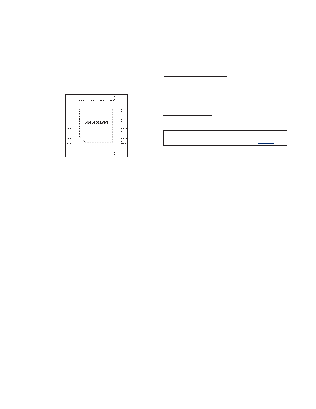
PACKAGE TYPE PACKAGE CODE DOCUMENT NO.
16 TQFN T1633+4
21-0136
Chip Information
PROCESS: BiCMOS
Pin Configuration
TOP VIEW
PGND
13
14
PGND
IN
*EXPOSED PAD, CONNECT TO SGND.
15
16
IN
LX
LX
12 11 9
MAX15041
+
12
DD
V
PGOOD
TQFN
BST
10
8
7
6
*EP
3
EN LX
5
4
COMP
I.C.
SGND
SS
FB
 Loading...