

Page 1
General Description
The MAX15038 high-efficiency switching regulator
delivers up to 4A load current at output voltages from
0.6V to 90% of VIN. The IC operates from 2.9V to 5.5V,
making it ideal for on-board point-of-load and postregulation applications. Total output error is less than ±1%
over load, line, and temperature ranges.
The MAX15038 features fixed-frequency PWM mode
operation with a switching frequency range of 500kHz
to 2MHz set by an external resistor. The MAX15038
provides the option of operating in a pulse-skip mode
to improve light-load efficiency. High-frequency operation allows for an all-ceramic capacitor design. The
high operating frequency also allows for small-size
external components.
The low-resistance on-chip nMOS switches ensure high
efficiency at heavy loads while minimizing critical inductances, making the layout a much simpler task with
respect to discrete solutions. Following a simple layout
and footprint ensures first-pass success in new designs.
The MAX15038 comes with a high bandwidth (28MHz)
voltage-error amplifier. The voltage-mode control architecture and the voltage-error amplifier permit a type III
compensation scheme to be utilized to achieve maximum loop bandwidth, up to 20% of the switching frequency. High loop bandwidth provides fast transient
response, resulting in less required output capacitance
and allowing for all-ceramic-capacitor designs.
The MAX15038 provides two three-state logic inputs to
select one of nine preset output voltages. The preset
output voltages allow customers to achieve ±1% output-voltage accuracy without using expensive 0.1%
resistors. In addition, the output voltage can be set to
any customer value by either using two external resistors at the feedback with a 0.6V internal reference or
applying an external reference voltage to the REFIN
input. The MAX15038 offers programmable soft-start
time using one capacitor to reduce input inrush current.
Applications
Server Power Supplies
POLs
ASIC/CPU/DSP Core and I/O Voltages
DDR Power Supplies
Base-Station Power Supplies
Telecom and Networking Power Supplies
RAID Control Power Supplies
Features
o Internal 31mΩ R
DS(ON)
High-Side and 24mΩ
R
DS(ON)
Low-Side MOSFETs
o Continuous 4A Output Current Over Temperature
o ±1% Output Accuracy Over Load, Line, and
Temperature
o Operates from 2.9V to 5.5V V
IN
Supply
o Adjustable Output from 0.6V to (0.9 x VIN)
o Soft-Start Reduces Inrush Supply Current
o 500kHz to 2MHz Adjustable Switching Frequency
o Compatible with Ceramic, Polymer, and
Electrolytic Output Capacitors
o Nine Preset and Adjustable Output Voltages
0.6V, 0.7V, 0.8V, 1.0V, 1.2V, 1.5V, 1.8V, 2.0V,
2.5V, and Adjustable
o Monotonic Startup for Safe-Start into Prebiased
Outputs
o Selectable Forced PWM or Skip Mode for Light
Load Efficiency
o Overcurrent and Overtemperature Protection
o Output Current Sink/Source Capable with Cycle-
by-Cycle Protection
o Open-Drain Power-Good Output
o Lead-Free, 4mm x 4mm, 24-Pin Thin QFN Package
MAX15038
4A, 2MHz Step-Down Regulator
with Integrated Switches
________________________________________________________________
Maxim Integrated Products
1
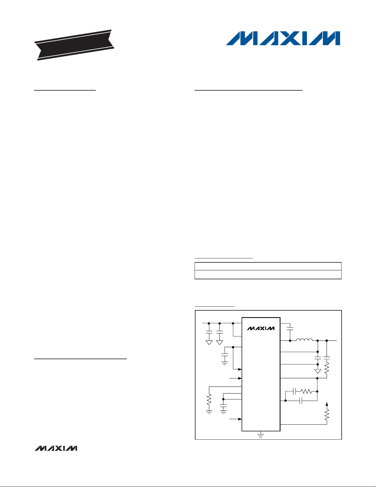
Typical Operating Circuit
Ordering Information
19-4320; Rev 0; 10/08
For pricing, delivery, and ordering information, please contact Maxim Direct at 1-888-629-4642,
or visit Maxim’s website at www.maxim-ic.com.
+
Denotes a lead-free/RoHS-compliant package.
*
EP = Exposed pad.
Pin Configuration appears at end of data sheet.
EVALUATION KIT
AVAILABLE
PART TEMP RANGE PIN-PACKAGE
MAX15038ETG+ -40°C to +85°C 24 Thin QFN-EP*
INPUT
2.9V TO 5.5V
IN
EN
V
DD
CTL2
CTL1
FREQ
REFIN
SS
MODE
MAX15038
GND
BST
OUT
PGND
COMP
PWRGD
OUTPUT
V
1.8V, 4A
DD
LX
FB
Page 2
MAX15038
4A, 2MHz Step-Down Regulator
with Integrated Switches
2 _______________________________________________________________________________________
ABSOLUTE MAXIMUM RATINGS
ELECTRICAL CHARACTERISTICS
(VIN= VEN= 5V, C
VDD
= 2.2µF, TA= TJ= -40°C to +85°C, typical values are at TA= +25°C, circuit of Figure 1, unless otherwise
noted.) (Note 3)
Stresses beyond those listed under “Absolute Maximum Ratings” may cause permanent damage to the device. These are stress ratings only, and functional
operation of the device at these or any other conditions beyond those indicated in the operational sections of the specifications is not implied. Exposure to
absolute maximum rating conditions for extended periods may affect device reliability.
IN, PWRGD to GND..................................................-0.3V to +6V
V
DD
to GND..................-0.3V to the lower of +4V or (VIN+ 0.3V)
COMP, FB, MODE, REFIN, CTL1, CTL2, SS,
FREQ to GND ..........................................-0.3V to (V
DD
+ 0.3V)
OUT, EN to GND ......................................................-0.3V to +6V
BST to LX..................................................................-0.3V to +6V
BST to GND ............................................................-0.3V to +12V
PGND to GND .......................................................-0.3V to +0.3V
LX to PGND ..................-0.3V to the lower of +6V or (V
IN
+ 0.3V)
LX to PGND ..........-1V to the lower of +6V or (V
IN
+ 1V) for 50ns
I
LX(RMS)
(Note 1) ......................................................................4A
V
DD
Output Short-Circuit Duration .............................Continuous
Converter Output Short-Circuit Duration ....................Continuous
Continuous Power Dissipation (T
A
= +70°C)
24-Pin TQFN (derate 27.8mW/°C above +70°C) ........2222mW
Thermal Resistance (Note 2)
θ
JA
.................................................................................36°C/W
θ
JC
..................................................................................6°C/W
Operating Temperature Range ...........................-40°C to +85°C
Junction Temperature......................................................+150°C
Storage Temperature Range .............................-65°C to +150°C
Lead Temperature (soldering, 10s) .................................+300°C
Note 1: LX has internal clamp diodes to PGND and IN. Applications that forward bias these diodes should take care not to exceed
the IC’s package power dissipation limits.
Note 2: Package thermal resistances were obtained using the method described in JEDEC specification JESD51-7, using a four-
layer board. For detailed information on package thermal considerations, refer to www.maxim-ic.com/thermal-tutorial
.
IN
IN Voltage Range 2.9 5.5 V
IN Supply Current fS = 1MHz, no load
Total Shutdown Current from IN
3.3V LDO (VDD)
VDD Undervoltage Lockout
Threshold
VDD Output Voltage VIN = 5V, I
VDD Dropout VIN = 2.9V, I
V
DD
BST
BST Supply Current V
PWM COMPARATOR
PWM Comparator Propagation
Delay
PWM Peak-to-Peak Ramp
Amplitude
PWM Valley Amplitude 0.8 V
PARAMETER CONDITIONS MIN TYP MAX UNITS
Current Limit VIN = 5V, VDD = 0 25 40 mA
VIN = 5V, VEN = 0 10 20
= VDD = 3.3V, VEN = 0 45
V
IN
LX starts/stops switching
= 0 to 10mA 3.1 3.3 3.5 V
VDD
= 10mA 0.08 V
VDD
= VIN = 5V, VLX = 0 or 5V, VEN = 0 0.025 µA
BST
10mV overdrive 20 ns
VIN = 3.3V 4.7 8
= 5V 5 8.5
V
IN
VDD rising 2.6 2.8
VDD falling 2.35 2.55
Minimum glitch-width
rejection
10 µs
1V
mA
µA
V
Page 3
MAX15038
4A, 2MHz Step-Down Regulator
with Integrated Switches
_______________________________________________________________________________________ 3
ELECTRICAL CHARACTERISTICS (continued)
(VIN= VEN= 5V, C
VDD
= 2.2µF, TA= TJ= -40°C to +85°C, typical values are at TA= +25°C, circuit of Figure 1, unless otherwise
noted.) (Note 3)
PARAMETER CONDITIONS MIN TYP MAX UNITS
ERROR AMPLIFIER
COMP Clamp Voltage, High VIN = 2.9V to 5V, VFB = 0.5V, V
COMP Clamp Voltage, Low VIN = 2.9V to 5V, VFB = 0.7V, V
COMP Slew Rate VFB step from 0.5V to 0.7V in 10ns 1.6 V/µs
COMP Shutdown Resistance
Internally Preset Output Voltage
Accuracy
FB Set Point Value CTL1 = CTL2 = GND, MODE = GND 0.594 0.6 0.606 V
FB to OUT Resistor All VID settings except CTL1 = CTL2 = GND 5.5 8 10.5 kΩ
Open-Loop Voltage Gain 115 dB
Error-Amplifier Unity-Gain
Bandwidth
Error-Amplifier Common-Mode
Input Range
Error-Amplifier Maximum Output
Current
FB Input Bias Current CTL1 = CTL2 = GND -125 nA
CTL_
CTL_ Input Bias Current
CTL_ Input Threshold
Hysteresis All VID transitions 50 mV
REFIN
REFIN Input Bias Current V
REFIN Offset Voltage V
LX (All Pins Combined)
LX On-Resistance, High-Side ILX = -2A
LX On-Resistance, Low-Side ILX = 2A
LX Leakage Current VIN = 5V, VEN = 0
= 0.6V 2 V
REFIN
= 0.6V 0.7 V
REFIN
From COMP to GND, V
V
= VSS = 0
EN
V
= VSS, MODE = GND -1 +1 %
REFIN
V
= 2.9V to 3.5V 0 V
DD
V
= 1V,
COMP
V
= 0.6V
REFIN
V
= 0 -7.2
CTL_
= V
V
CTL_
Low, falling 0.8
Float VDD/2
High, rising
REFIN
REFIN
High-side sourcing 5.7 7
Low-side sinking 7LX Current-Limit Threshold
Zero-crossing current threshold, MODE = V
DD
= 0.6V -185 nA
= 0.9V, FB shorted to COMP -4.5 +4.5 mV
= 3.3V, V
IN
VFB = 0.7V, sinking 1
V
= 0.5V, sourcing -1
FB
VIN = V
V
IN
VIN = 3.3V 30
V
IN
- VLX = 3.3V 42
BST
= V
- VLX = 5V 31 54
BST
= 5V 24 42
= 100mV,
COMP
DD
VLX = 0 -0.01
= 5V +0.01
V
LX
6 Ω
28 MHz
+7.2
V
-
DD
0.8
0.2
- 2 V
DD
mA
µA
V
mΩ
mΩ
A
µA
Page 4
MAX15038
4A, 2MHz Step-Down Regulator
with Integrated Switches
4 _______________________________________________________________________________________
ELECTRICAL CHARACTERISTICS (continued)
(VIN= VEN= 5V, C
VDD
= 2.2µF, TA= TJ= -40°C to +85°C, typical values are at TA= +25°C, circuit of Figure 1, unless otherwise
noted.) (Note 3)
LX Switching Frequency V
Switching Frequency Range 500 2000 kHz
LX Minimum Off-Time 78 ns
LX Maximum Duty Cycle R
LX Minimum Duty Cycle R
Average Short-Circuit IN Supply
Current
RMS LX Output Current 4A
ENABLE
EN Input Logic-Low Threshold EN falling 0.9 V
EN Input Logic-High Threshold EN rising 1.5 V
EN Input Current VEN = 0 or 5V, VIN = 5V 0.01 µA
MODE
MODE Input-Logic Hysteresis MODE falling 5 % V
MODE Input Bias Current
SS
SS Current VSS = 0.45V, V
THERMAL SHUTDOWN
Thermal-Shutdown Threshold Rising 165 °C
Thermal-Shutdown Hysteresis 25 °C
POWER-GOOD (PWRGD)
Power-Good Threshold Voltage
Power-Good Edge Deglitch VFB rising or falling 48
PWRGD Output Voltage Low I
PWRGD Leakage Current VIN = V
HICCUP OVERCURRENT LIMIT
Current-Limit Startup Blanking 112
Autoretry Restart Time 896
PARAMETER CONDITIONS MIN TYP MAX UNITS
R
= 49.9kΩ 0.9 1 1.1
= 2.9V to 5V
IN
= 49.9kΩ 92 95 %
FREQ
= 49.9kΩ 515%
FREQ
OUT connected to GND, V
Logic-low, falling 26
Logic VDD/2 or floating, rising 50MODE Input-Logic Threshold
Logic-high, rising 74
MODE = GND -5
MODE = V
VFB falling, V
V
FB
PWRGD
DD
= 0.6V, sourcing 6.7 8 9.3 µA
REFIN
= 0.6V 88 90 92
REFIN
rising, V
= 4mA 0.03 0.1 V
PWRGD
= 0.6V 92.5
REFIN
= 5V, VFB = 0.7V, V
= 5V 0.15 A
IN
FREQ
= 23.6kΩ 1.8 2 2.2
R
FREQ
5
= 0.6V 0.01 µA
REFIN
MHz
% V
DD
DD
µA
%
V
REFIN
Clock
cycles
Clock
cycles
Clock
cycles
Page 5
MAX15038
4A, 2MHz Step-Down Regulator
with Integrated Switches
_______________________________________________________________________________________
5
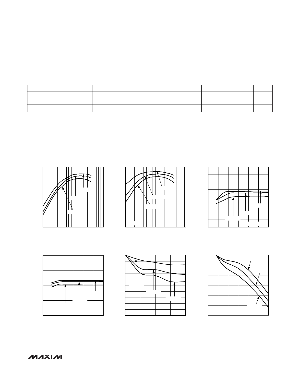
Typical Operating Characteristics
(Typical values are VIN= VEN= 5V, V
OUT
= 1.8V, R
FREQ
= 49.9kΩ, I
OUT
= 4A, TA= +25°C, circuit of Figure 1, unless otherwise noted.)
ELECTRICAL CHARACTERISTICS (continued)
(VIN= VEN= 5V, C
VDD
= 2.2µF, TA= TJ= -40°C to +85°C, typical values are at TA= +25°C, circuit of Figure 1, unless otherwise
noted.) (Note 3)
Note 3: Specifications are 100% production tested at TA= +25°C. Limits over the operating temperature range are guaranteed by design.
PARAMETER CONDITIONS MIN TYP MAX UNITS
FB Hiccup Threshold VFB falling 70
Hiccup Threshold Blanking Time VFB falling 28 µs
V
REFIN
%
EFFICIENCY
vs. OUTPUT CURRENT
100
90
80
70
EFFICIENCY (%)
60
50
40
0.1 10.0
OUTPUT CURRENT (A)
V
= 2.5V
OUT
V
= 1.8V
OUT
V
= 1.2V
OUT
1.0
MAX15038 toc01
EFFICIENCY
vs. OUTPUT CURRENT
100
90
80
70
EFFICIENCY (%)
60
50
VIN = 3.3V
40
0.1 10.0
OUTPUT CURRENT (A)
V
= 2.5V
OUT
V
= 1.8V
OUT
V
= 1.2V
OUT
1.0
MAX15038 toc02
FREQUENCY (MHz)
FREQUENCY
vs. INPUT VOLTAGE
2.20
2.15
2.10
2.05
2.00
1.95
1.90
1.85
1.80
2.5 5.5
TA = -40°C
INPUT VOLTAGE (V)
TA = +25°C
R
TA = +85°C
FREQ
= 23.2k
5.04.53.0 3.5 4.0
Ω
MAX15038 toc03
FREQUENCY
vs. INPUT VOLTAGE
1.20
1.15
1.10
1.05
1.00
0.95
FREQUENCY (MHz)
0.90
0.85
0.80
2.5 5.5
TA = +25°C
TA = -40°C
INPUT VOLTAGE (V)
R
FREQ
TA = +85°C
= 49.9k
5.04.53.0 3.5 4.0
Ω
0
-0.05
-0.10
MAX15038 toc04
-0.15
-0.20
V
-0.25
-0.30
-0.35
OUTPUT-VOLTAGE CHANGE (%)
-0.40
-0.45
-0.50
OUT
04
LOAD REGULATION
= 1.2V
V
= 1.8V
OUT
LOAD CURRENT (A)
LINE REGULATION (LOAD = 4A)
0
-0.02
MAX15038 toc05a
-0.04
-0.06
V
= 2.5V
OUT
321
-0.08
OUTPUT-VOLTAGE CHANGE (%)
-0.10
-0.12
2.5 5.5
INPUT VOLTAGE (V)
V
= 2.5V
OUT
= 1.8V
5.04.54.03.53.0
MAX15038 toc05b
V
OUT
V
= 1.2V
OUT
Page 6
MAX15038
4A, 2MHz Step-Down Regulator
with Integrated Switches
6 _______________________________________________________________________________________
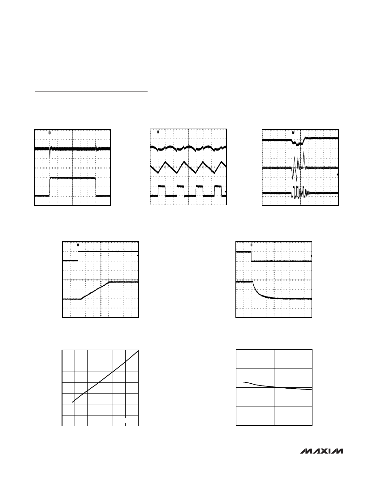
Typical Operating Characteristics (continued)
(Typical values are VIN= VEN= 5V, V
OUT
= 1.8V, R
FREQ
= 49.9kΩ, I
OUT
= 4A, TA= +25°C, circuit of Figure 1, unless otherwise noted.)
LOAD TRANSIENT
MAX15038 toc06
40µs/div
V
OUT
AC-COUPLED
100mV/div
2A
I
OUT
0A
SWITCHING WAVEFORMS
(FORCED PWM, 2A LOAD)
MAX15038 toc07
400ns/div
AC-COUPLED
50mV/div
V
OUT
I
LX
V
LX
2A/div
0A
5V/div
SWITCHING WAVEFORMS
(SKIP MODE, NO LOAD)
MAX15038 toc08
2µs/div
AC-COUPLED
100mV/div
V
OUT
I
LX
V
LX
1A/div
0A
0V
5V/div
SOFT-START WAVEFORM
(R
LOAD
= 0.5Ω)
MAX15038 toc09
400µs/div
V
EN
5V/div
0V
V
OUT
1V/div
SHUTDOWN WAVEFORM
(R
LOAD
= 0.5Ω)
MAX15038 toc10
10µs/div
V
EN
5V/div
0V
V
OUT
1V/div
INPUT SHUTDOWN CURRENT
vs. INPUT VOLTAGE
MAX15038 toc11
INPUT VOLTAGE (V)
INPUT SHUTDOWN CURRENT (µA)
5.04.54.03.53.0
6
7
8
9
10
11
12
5
2.5 5.5
VEN = 0V
MAXIMUM OUTPUT CURRENT
vs. OUTPUT VOLTAGE
MAX15038 toc12
OUTPUT VOLTAGE (V)
MAXIMUM OUTPUT CURRENT (A)
2.01.51.0
3
4
5
6
7
8
9
10
2
0.5 2.5
Page 7

MAX15038
4A, 2MHz Step-Down Regulator
with Integrated Switches
_______________________________________________________________________________________
7
Typical Operating Characteristics (continued)
(Typical values are VIN= VEN= 5V, V
OUT
= 1.8V, R
FREQ
= 49.9kΩ, I
OUT
= 4A, TA= +25°C, circuit of Figure 1, unless otherwise noted.)
HICCUP CURRENT LIMIT
MAX15038 toc13
400µs/div
1V/div
5A/div
1A/div
0V
0A
0A
V
OUT
I
OUT
I
IN
RMS INPUT CURRENT DURING
SHORT CIRCUIT vs. INPUT VOLTAGE
MAX15038 toc14
INPUT VOLTAGE (V)
RMS INPUT CURRENT (A)
5.04.54.03.53.0
0.1
0.2
0.3
0.4
0.5
0
2.5 5.5
V
OUT
= 0V
EXPOSED PAD TEMPERATURE
vs. AMBIENT TEMPERATURE
MAX15038 toc15
AMBIENT TEMPERATURE (°C)
EXPOSED PAD TEMPERATURE (°C)
80604020
10
20
30
40
50
60
70
80
90
100
0
0 100
MEASURED ON A MAX15038EVKIT
4A LOAD
FEEDBACK VOLTAGE
vs. TEMPERATURE
MAX15038 toc16
TEMPERATURE (°C)
FEEDBACK VOLTAGE (V)
6035-15 10
0.57
0.58
0.59
0.60
0.62
0.61
0.63
0.64
0.56
-40 85
SOFT-START WITH REFIN
MAX15038 toc17
200µs/div
1A/div
0.5V/div
2V/div
0A
1V/div
0V
0V
0V
I
IN
V
PWRGD
V
REFIN
V
OUT
STARTING INTO PREBIASED OUTPUT
(MODE = V
DD
, V
OUT
= 2.5V, 2A LOAD)
MAX15038 toc18
200µs/div
5V/div
1V/div
5V/div
0V
2A
0A
0V
0V
V
EN
V
PWRGD
V
OUT
I
OUT
STARTING INTO PREBIASED OUTPUT
(MODE = V
DD
/2, V
OUT
= 2.5V, 2A LOAD)
MAX15038 toc19
200µs/div
5V/div
1V/div
5V/div
0V
2A
0A
0V
0V
V
EN
V
PWRGD
V
OUT
I
OUT
Page 8

MAX15038
4A, 2MHz Step-Down Regulator
with Integrated Switches
8 _______________________________________________________________________________________
Typical Operating Characteristics (continued)
(Typical values are VIN= VEN= 5V, V
OUT
= 1.8V, R
FREQ
= 49.9kΩ, I
OUT
= 4A, TA= +25°C, circuit of Figure 1, unless otherwise noted.)
STARTING INTO PREBIASED OUTPUT
(MODE = V
DD
, V
OUT
= 2.5V, NO LOAD)
MAX15038 toc20
200µs/div
V
EN
2V/div
V
OUT
1V/div
V
PWRGD
2V/div
0V
0V
0V
STARTING INTO PREBIASED OUTPUT
(MODE = V
DD
/2, V
OUT
= 2.5V, NO LOAD)
MAX15038 toc21
200µs/div
V
EN
2V/div
V
OUT
1V/div
V
PWRGD
2V/div
0V
0V
0V
STARTING INTO PREBIASED OUTPUT
ABOVE NOMINAL SETPOINT (V
OUT
= 1.5V)
MAX15038 toc22
1ms/div
V
EN
2V/div
V
OUT
1V/div
V
PWRGD
2V/div
0V
0V
0V
V
MODE
= VDD,
NO LOAD
STARTING INTO PREBIASED ABOVE
NOMINAL SETPOINT (V
OUT
= 1.5V)
MAX15038 toc23
1ms/div
V
EN
2V/div
V
OUT
1V/div
V
PWRGD
2V/div
0V
0V
0V
V
MODE
= VDD/2,
NO LOAD
TRANSITION FROM SKIP MODE
TO FORCED PWM MODE
MAX15038 toc24
2ms/div
V
MODE
5V/div
V
LX
5V/div
V
OUT
0.5V/div
0V
TRANSITION FROM FORCED PWM
TO SKIP MODE
MAX15038 toc25
4ms/div
V
MODE
5V/div
V
LX
5V/div
V
OUT
0.5V/div
0V
Page 9

MAX15038
4A, 2MHz Step-Down Regulator
with Integrated Switches
_______________________________________________________________________________________ 9
Pin Description
PIN NAME FUNCTION
1 MODE Functional MODE Selection Input. See the MODE Selection section for more information.
2V
3 CTL1
4 CTL2
5 REFIN
6SS
7 GND
8 COMP
9FB
10 OUT
11 FREQ
3.3V LDO Output. Supply input for the internal analog core. Connect a low-ESR, ceramic capacitor with a
DD
minimum value of 2.2µF from V
Preset Output-Voltage Selection Inputs. CTL1 and CTL2 set the output voltage to one of nine preset
voltages. See Table 1 and the Programming the Output Voltage (CTL1, CTL2) section for preset voltages.
External Reference Input. Connect REFIN to SS to use the internal 0.6V reference. Connecting REFIN to an
external voltage forces FB to regulate to the voltage applied to REFIN. REFIN is internally pulled to GND
when the IC is in shutdown/hiccup mode.
Soft-Start Input. Connect a capacitor from SS to GND to set the startup time. Use a capacitor with a 1nF
minimum value. See the Soft-Start and REFIN section for details on setting the soft-start time.
Analog Ground Connection. Connect GND and PGND together at one point near the input bypass capacitor
return terminal.
Voltage Error-Amplifier Output. Connect the necessary compensation network from COMP to FB and OUT.
COMP is internally pulled to GND when the IC is in shutdown/hiccup mode.
Feedback Input. Connect FB to the center tap of an external resistive divider from the output to GND to set
the output voltage from 0.6V to 90% of V
CTL1 and CTL2 to select any of nine preset voltages.
Output-Voltage Sense. Connect to the converter output. Leave OUT unconnected when an external resistive
divider is used.
Oscillator Frequency Select. Connect a precision resistor from FREQ to GND to select the switching
frequency. See the Frequency Select (FREQ) section.
to GND.
DD
. Connect FB through an RC network to the output when using
IN
Open-Drain, Power-Good Output. PWRGD is high impedance when V
12 PWRGD
13 BST
14, 15,
16
17–20 PGND
21, 22,
23
24 EN Enable Input. Logic input to enable/disable the MAX15038.
—EP
LX
IN
and V
V
REFIN
internal UVLO threshold, or the IC is in thermal shutdown.
High-Side MOSFET Driver Supply. Internally connected to IN through a PMOS switch. Bypass BST to LX with
a 0.1µF capacitor.
Inductor Connection. All LX pins are internally shorted together. Connect all LX pins to the switched side of
the inductor. LX is high impedance when the IC is in shutdown mode.
Power Ground. Connect all PGND pins externally to the power ground plane. Connect all PGND pins
together near the IC.
Input Power Supply. Input supply range is from 2.9V to 5.5V. Bypass IN to PGND with a 22µF ceramic
capacitor.
Exposed Pad. Solder EP to a large contiguous copper plane connected to PGND to optimize thermal
performance. Do not use EP as a ground connection for the device.
is above 0.54V. PWRGD is internally pulled low when VFB falls below 90% (typ) of V
REFIN
is below 0.54V. PWRGD is internally pulled low when the IC is in shutdown mode, VDD is below the
rises above 92.5% (typ) of V
FB
REFIN
REFIN
or
Page 10

MAX15038
4A, 2MHz Step-Down Regulator
with Integrated Switches
10 ______________________________________________________________________________________
Block Diagram
V
DD
EN
SS
REFIN
OUT
8kΩ
FB
SHUTDOWN
CONTROL
BIAS
GENERATOR
VOLTAGE
REFERENCE
SOFT-START
ERROR
AMPLIFIER
UVLO
CIRCUITRY
THERMAL
SHUTDOWN
3.3V LDO
PWM
COMPARATOR
CURRENT-LIMIT
COMPARATOR
CONTROL
LOGIC
MAX15038
IN
CURRENT-LIMIT
COMPARATOR
BST SWITCH
BST
IN
LX
PGND
MODE
CTL1
CTL2
COMP
VOLTAGECONTROL
CIRCUITRY
VID
COMP CLAMPS
0.9 x V
1V
P-P
FB
REFIN
OSCILLATOR
SHDN
FREQ
PWRGD
GND
Page 11

MAX15038
Figure 1. 1MHz, All-Ceramic-Capacitor Design with VIN= 2.9V to 5.5V and V
OUT
= 1.8V
Detailed Description
The MAX15038 high-efficiency, voltage-mode switching
regulator delivers up to 4A of output current. The
MAX15038 provides output voltages from 0.6V to 0.9 x
VINfrom 2.9V to 5.5V input supplies, making it ideal for
on-board point-of-load applications. The output voltage
accuracy is better than ±1% over load, line, and temperature.
The MAX15038 features a wide switching frequency
range, allowing the user to achieve all-ceramic-capacitor designs and fast transient responses (see Figure 1).
The high operating frequency minimizes the size of
external components. The MAX15038 is available in a
small (4mm x 4mm), lead-free, 24-pin thin QFN package. The REFIN function makes the MAX15038 an ideal
candidate for DDR and tracking power supplies. Using
internal low-R
DS(ON)
(24mΩ for the low-side n-channel
MOSFET and 31mΩ for the high-side n-channel
MOSFET) maintains high efficiency at both heavy-load
and high-switching frequencies.
The MAX15038 employs voltage-mode control architecture with a high bandwidth (28MHz) error amplifier. The
voltage-mode control architecture allows up to 2MHz
switching frequency, reducing board area. The op-amp
voltage-error amplifier works with type III compensation
to fully utilize the bandwidth of the high-frequency
switching to obtain fast transient response. Adjustable
soft-start time provides flexibilities to minimize input
startup inrush current. An open-drain, power-good
(PWRGD) output goes high when V
FB
reaches 92.5% of
V
REFIN
and V
REFIN
is greater than 0.54V.
The MAX15038 provides option for three modes of operation: regular PWM, PWM mode with monotonic startup
into prebiased output, or skip mode with monotonic
startup into prebiased output.
Typical Application Circuit
4A, 2MHz Step-Down Regulator
with Integrated Switches
______________________________________________________________________________________ 11
INPUT
2.9V TO 5.5V
C6
22µF
0.1µF
C7
49.9kΩ
R4
2.2µF
2.2Ω
IN
MAX15038
V
C5
C4
0.022µF
DD
CTL2
CTL1
EN
FREQ
REFIN
SS
MODE
GND
BST
OUT
PGND
COMP
PWRGD
C10
0.1µF
LX
FB
C2
1500pF
C1
33pF
R2
2.67kΩ
L1
0.47µH
560pF
158Ω
C3
R3
V
DD
R1
20kΩ
C15
1000pF
C8
22µF
OPTIONAL
OUTPUT
1.8V, 4A
C9
0.01µF
Page 12

Controller Function
The controller logic block is the central processor that
determines the duty cycle of the high-side MOSFET
under different line, load, and temperature conditions.
Under normal operation, where the current-limit and
temperature protection are not triggered, the controller
logic block takes the output from the PWM comparator
and generates the driver signals for both high-side and
low-side MOSFETs. The break-before-make logic and
the timing for charging the bootstrap capacitors are
calculated by the controller logic block. The error signal
from the voltage-error amplifier is compared with the
ramp signal generated by the oscillator at the PWM
comparator and, thus, the required PWM signal is produced. The high-side switch is turned on at the beginning of the oscillator cycle and turns off when the ramp
voltage exceeds the V
COMP
signal or the current-limit
threshold is exceeded. The low-side switch is then
turned on for the remainder of the oscillator cycle.
Current Limit
The internal, high-side MOSFET has a typical 7A peak
current-limit threshold. When current flowing out of LX
exceeds this limit, the high-side MOSFET turns off and
the synchronous rectifier turns on. The synchronous
rectifier remains on until the inductor current falls below
the low-side current limit. This lowers the duty cycle
and causes the output voltage to droop until the current
limit is no longer exceeded. The MAX15038 uses a hiccup mode to prevent overheating during short-circuit
output conditions.
During current limit, if VFBdrops below 70% of REFIN
and stays below this level for 12µs or more, the
MAX15038 enters hiccup mode. The high-side
MOSFET and the synchronous rectifier are turned off
and both COMP and REFIN are internally pulled low. If
REFIN and SS are connected together, both are pulled
low. The part remains in this state for 896 clock cycles
and then attempts to restart for 112 clock cycles. If the
fault causing current limit has cleared, the part resumes
normal operation. Otherwise, the part reenters hiccup
mode again.
Soft-Start and REFIN
The MAX15038 utilizes an adjustable soft-start function
to limit inrush current during startup. An 8µA (typ) current source charges an external capacitor connected to
SS. The soft-start time is adjusted by the value of the
external capacitor from SS to GND. The required
capacitance value is determined as:
where tSSis the required soft-start time in seconds. The
MAX15038 also features an external reference input
(REFIN). The IC regulates FB to the voltage applied to
REFIN. The internal soft-start is not available when
using an external reference. A method of soft-start
when using an external reference is shown in Figure 2.
Connect REFIN to SS to use the internal 0.6V reference.
Use a capacitor of 1nF minimum value at SS.
Undervoltage Lockout (UVLO)
The UVLO circuitry inhibits switching when VDDis below
2.55V (typ). Once VDDrises above 2.6V (typ), UVLO
clears and the soft-start function activates. A 50mV hysteresis is built in for glitch immunity.
BST
The gate-drive voltage for the high-side, n-channel
switch is generated by a flying-capacitor boost circuit.
The capacitor between BST and LX is charged from the
VINsupply while the low-side MOSFET is on. When the
low-side MOSFET is switched off, the voltage of the
capacitor is stacked above LX to provide the necessary
turn-on voltage for the high-side internal MOSFET.
Frequency Select (FREQ)
The switching frequency is resistor programmable from
500kHz to 2MHz. Set the switching frequency of the IC
with a resistor (R
FREQ
) connected from FREQ to GND.
R
FREQ
is calculated as:
where fSis the desired switching frequency in Hertz.
Figure 2. Typical Soft-Start Implementation with External
Reference
MAX15038
4A, 2MHz Step-Down Regulator
with Integrated Switches
12 ______________________________________________________________________________________
At
×806µ
C
=
SS
V
.
R1
R
R2
FREQ
k
50
=×−
095
.
C
1
Ω
sf
µ
005
(.)
S
REFIN
MAX15038
s
µ
Page 13

MAX15038
Power-Good Output (PWRGD)
PWRGD is an open-drain output that goes high impedance when VFBis above 0.925 x V
REFIN
and V
REFIN
is
above 0.54V for at least 48 clock cycles. PWRGD pulls
low when V
FB
is below 90% of V
REFIN
or V
REFIN
is
below 0.54V for at least 48 clock cycles. PWRGD is low
when the IC is in shutdown mode, V
DD
is below the
internal UVLO threshold, or the IC is in thermal shutdown mode.
Programming the Output Voltage
(CTL1, CTL2)
As shown in Table 1, the output voltage is pin programmable by the logic states of CTL1 and CTL2. CTL1 and
CTL2 are trilevel inputs: VDD, unconnected, and GND.
An 8.06kΩ resistor must be connected between OUT
and FB when CTL1 and CTL2 are connected to GND.
The logic states of CTL1 and CTL2 should be programmed only before power-up. Once the part is
enabled, CTL1 and CTL2 should not be changed. If the
output voltage needs to be reprogrammed, cycle
power or EN and reprogram before enabling. The output voltage can be programmed continuously from
0.6V to 90% of VINby using a resistor-divider network
from OUT to FB to GND as shown in Figure 3a. CTL1
and CTL2 must be connected to GND.
Shutdown Mode
Drive EN to GND to shut down the IC and reduce quiescent current to a typical value of 10µA. During shutdown,
the LX is high impedance. Drive EN high to enable the
MAX15038.
Thermal Protection
Thermal-overload protection limits total power dissipation
in the device. When the junction temperature exceeds
TJ= +165°C, a thermal sensor forces the device into
shutdown, allowing the die to cool. The thermal sensor
turns the device on again after the junction temperature
cools by 20°C, causing a pulsed output during continuous overload conditions. The soft-start sequence begins
after recovery from a thermal-shutdown condition.
Applications Information
IN and VDDDecoupling
To decrease the noise effects due to the high switching
frequency and maximize the output accuracy of
the MAX15038, decouple VINwith a 22µF capacitor
from VINto PGND. Also decouple VDDwith a 2.2µF
low-ESR ceramic capacitor from V
DD
to GND. Place
these capacitors as close as possible to the IC.
Inductor Selection
Choose an inductor with the following equation:
where LIR is the ratio of the inductor ripple current to full
load current at the minimum duty cycle. Choose LIR
between 20% to 40% for best performance and stability.
Use an inductor with the lowest possible DC resistance
that fits in the allotted dimensions. Powdered iron ferrite
core types are often the best choice for performance.
With any core material, the core must be large enough
not to saturate at the current limit of the MAX15038.
Output-Capacitor Selection
The key selection parameters for the output capacitor are
capacitance, ESR, ESL, and voltage-rating requirements.
These affect the overall stability, output ripple voltage,
and transient response of the DC-DC converter. The output ripple occurs due to variations in the charge stored
in the output capacitor, the voltage drop due to the
capacitor’s ESR, and the voltage drop due to the
capacitor’s ESL. Estimate the output-voltage ripple due
to the output capacitance, ESR, and ESL:
VV V V
RIPPLE RIPPLE C RIPPLE ESR RIPPLE ESL
=+ +
() ( ) ( ))
Table 1. CTL1 and CTL2 Output Voltage
Selection
4A, 2MHz Step-Down Regulator
with Integrated Switches
______________________________________________________________________________________ 13
CTL1 CTL2 V
GND GND 0.6
V
DD
GND Unconnected 0.8
GND V
Unconnected GND 1.2
Unconnected Unconnected 1.5
Unconnected V
V
DD
V
DD
V
DD
DD
DD
GND 2.0
Unconnected 2.5
VVV
×−
()
L
OUT IN OUT
=
f V LIR I
×××
S IN OUT MAX
()
OUT
0.7
1.0
1.8
(V)
Page 14

MAX15038
4A, 2MHz Step-Down Regulator
with Integrated Switches
14 ______________________________________________________________________________________
where the output ripple due to output capacitance,
ESR, and ESL is:
or:
or whichever is larger.
The peak-to-peak inductor current (I
P-P
) is:
Use these equations for initial output capacitor selection. Determine final values by testing a prototype or an
evaluation circuit. A smaller ripple current results in less
output-voltage ripple. Since the inductor ripple current
is a factor of the inductor value, the output-voltage ripple decreases with larger inductance. Use ceramic
capacitors for low ESR and low ESL at the switching
frequency of the converter. The ripple voltage due to
ESL is negligible when using ceramic capacitors.
Load-transient response depends on the selected output capacitance. During a load transient, the output
instantly changes by ESR x ∆I
LOAD
. Before the controller can respond, the output deviates further,
depending on the inductor and output capacitor values. After a short time, the controller responds by regulating the output voltage back to its predetermined
value. The controller response time depends on the
closed-loop bandwidth. A higher bandwidth yields a
faster response time, preventing the output from deviating further from its regulating value. See the
Compen-
sation Design
section for more details.
Input-Capacitor Selection
The input capacitor reduces the current peaks drawn
from the input power supply and reduces switching
noise in the IC. The total input capacitance must be
equal or greater than the value given by the following
equation to keep the input-ripple voltage within
specification and minimize the high-frequency ripple
current being fed back to the input source:
where V
IN-RIPPLE
is the maximum allowed input ripple
voltage across the input capacitors and is recommended to be less than 2% of the minimum input voltage. D
is the duty cycle (V
OUT/VIN
) and TSis the switching
period (1/fS).
The impedance of the input capacitor at the switching
frequency should be less than that of the input source so
high-frequency switching currents do not pass through
the input source, but are instead shunted through the
input capacitor. The input capacitor must meet the ripple
current requirement imposed by the switching currents.
The RMS input ripple current is given by:
where I
RIPPLE
is the input RMS ripple current.
Compensation Design
The power transfer function consists of one double pole
and one zero. The double pole is introduced by the
inductor L and the output capacitor CO. The ESR of the
output capacitor determines the zero. The double pole
and zero frequencies are given as follows:
where RLis equal to the sum of the output inductor’s DCR
(DC resistance) and the internal switch resistance,
R
DS(ON)
. A typical value for R
DS(ON)
is 24mΩ (low-side
MOSFET) and 31mΩ (high-side MOSFET). ROis the output load resistance, which is equal to the rated output
voltage divided by the rated output current. ESR is the
total equivalent series resistance of the output capacitor.
If there is more than one output capacitor of the same
type in parallel, the value of the ESR in the above equation is equal to that of the ESR of a single output capacitor
divided by the total number of output capacitors.
V
RIPPLE C
VIxE
V
RIPPLE ESL
()
RIPPLE ESR P P()=−
()
=
xC xf
8
I
PP
=
t
ON
I
−
PP
OUT S
−
x ESL
SSR
I
V
RIPPLE ESLP()
VV
I
PP
IN OUTSOUT
=
−
fL
−PP
=
−
×
t
OFF
x ESL
V
x
V
IN
DxT xI
SOUT
V
IN RIPPLE
−
C
IN MIN
=
_
VVV
×−()
OUT IN OUT
V
IN
II
RIPPLE LOAD
=×
ff
==
PLC P LC
12
__
2
xLxC x
π
f
Z ESR
_
=
2π
1
⎛
O
⎜
⎝
1
x ESR x C
R ESR
O
RR
OL
O
⎞
+
⎟
+
⎠
Page 15

MAX15038
The high switching frequency range of the MAX15038
allows the use of ceramic output capacitors. Since the
ESR of ceramic capacitors is typically very low, the frequency of the associated transfer function zero is higher
than the unity-gain crossover frequency, fC, and the zero
cannot be used to compensate for the double pole created by the output filtering inductor and capacitor. The double pole produces a gain drop of 40dB/decade and a
phase shift of 180°. The compensation network error
amplifier must compensate for this gain drop and phase
shift to achieve a stable high-bandwidth closed-loop system. Therefore, use type III compensation as shown in
Figures 3 and 4. Type III compensation possesses three
poles and two zeros with the first pole, f
P1_EA
, located at
zero frequency (DC). Locations of other poles and zeros
of the type III compensation are given by:
The above equations are based on the assumptions
that C1 >> C2, and R3 >> R2, which are true in most
applications. Placements of these poles and zeros are
determined by the frequencies of the double pole and
ESR zero of the power transfer function. It is also a
function of the desired close-loop bandwidth. The following section outlines the step-by-step design procedure to calculate the required compensation
components for the MAX15038. When the output voltage of the MAX15038 is programmed to a preset voltage, R3 is internal to the IC and R4 does not exist
(Figure 3b).
When externally programming the MAX15038 (Figure
3a), the output voltage is determined by:
For a 0.6V output, connect an 80kΩ resistor from FB to
OUT. The zero-cross frequency of the close-loop, f
C
should be between 10% and 20% of the switching frequency, fS. A higher zero-cross frequency results in
faster transient response. Once fCis chosen, C1 is calculated from the following equation:
where V
P-P
is the ramp peak-to-peak voltage (1V typ).
Due to the underdamped nature of the output LC double
pole, set the two zero frequencies of the type III compensation less than the LC double-pole frequency to provide
adequate phase boost. Set the two zero frequencies to
80% of the LC double-pole frequency. Hence:
4A, 2MHz Step-Down Regulator
with Integrated Switches
______________________________________________________________________________________ 15
Figure 3. Type III Compensation Network
f
f
f
f
ZEA2
PEA3
PEA2
ZEA1
=
_
=
_
=
_
=
_
1
RC
××π
211
1
RC
××π
233
1
RC
××π
212
1
RC
××π
223
R
06 3
×
R
4
.
V
(.)
OUT
for V V
(.)
−
06
OUT
06=
>
V
IN
x
25
.
V
−
PP
R
L
+×
()π
R
O
C
1
=
xxRx
231
=
08 1
=
08 3
MAX15038
CTL1
CTL2
MAX15038
CTL1
CTL2
1
xC
1
xR
R3
8kΩ
R
1
C
3
VOLTAGE
SELECT
L x C x R ESR
x
OO
RR
L x C x R ESR
x
OO
RR
LX
OUT
FB
COMP
LX
OUT
FB
COMP
L
R1
a)
EXTERNAL RESISTIVE DIVIDER
L
R1
b)
INTERNAL PRESET VOLTAGES
+
()
+.
LO
+
()
+.
LO
C
OUT
C1
C2
C
OUT
C1
C2
f
C
V
OUT
R3
R4
R2
C3
V
OUT
R2
C3
Page 16

Setting the second compensation pole, f
P2_EA
, at
f
Z_ESR
yields:
Set the third compensation pole at 1/2 of the switching
frequency. Calculate C2 as follows:
The above equations provide application compensation
when the zero-cross frequency is significantly higher
than the double-pole frequency. When the zero-cross
frequency is near the double-pole frequency, the actual
zero-cross frequency is higher than the calculated frequency. In this case, lowering the value of R1 reduces
the zero-cross frequency. Also, set the third pole of the
type III compensation close to the switching frequency
if the zero-cross frequency is above 200kHz to boost
the phase margin. The recommended range for R3 is
2kΩ to 10kΩ. Note that the loop compensation remains
unchanged if only R4’s resistance is altered to set different outputs.
MODE Selection
The MAX15038 features a mode selection input
(MODE) that users can select a functional mode for the
device (see Table 2).
Forced-PWM Mode
Connect MODE to GND to select forced-PWM mode. In
forced-PWM mode, the MAX15038 operates at a constant switching frequency (set by the resistor at FREQ
terminal) with no pulse skipping. PWM operation starts
after a brief settling time when EN goes high. The lowside switch turns on first, charging the bootstrap capacitor to provide the gate-drive voltage for the high-side
switch. The low-side switch turns off either at the end of
the clock period or once the low-side switch sinks
0.875A current (typ), whichever occurs first. If the lowside switch is turned off before the end of the clock period, the high-side switch is turned on for the remaining
part of the time interval until the inductor current reaches
0.58A, or the end of clock cycle is encountered.
Starting from the first PWM activity, the sink current
threshold is increased through an internal 4-step DAC
to reach the current limit of 7A after 128 clock periods.
This is done to help a smooth recovery of the regulated
voltage even in case of accidental prebiased output in
spite of the initial forced-PWM mode selection.
Soft-Starting into a Prebiased Output
Mode (Monotonic Startup)
When MODE is left unconnected or biased to VDD/2, the
MAX15038 soft-starts into a prebiased output without discharging the output capacitor. This type of operation is
also termed monotonic startup. See the Starting into
Prebiased Output waveforms in the
Typical Operating
Characteristics
section for an example.
In monotonic startup mode, both low-side and highside switches remain off to avoid discharging the prebiased output. PWM operation starts when the FB voltage
crosses the SS voltage. As in forced-PWM mode, the
PWM activity starts with the low-side switch turning on
first to build the bootstrap capacitor charge.
The MAX15038 is also able to start into prebiased with
the output above the nominal set point without abruptly
discharging the output, thanks to the sink current control of the low-side switch through a 4-step DAC in 128
clock cycles. Monotonic startup mode automatically
switches to forced-PWM mode 4096 clock cycles delay
Figure 4. Type III Compensation Illustration
MAX15038
4A, 2MHz Step-Down Regulator
with Integrated Switches
16 ______________________________________________________________________________________
Table 2. Mode Selection
R
23=
C x ESR
O
C
C
2
1
R
1=×׃π
S
MODE CONNECTION OPERATION MODE
GND Forced PWM
Forced PWM. Soft-startup into a
Unconnected or VDD/2
V
DD
COMPENSATION
TRANSFER
FUNCTION
GAIN (dB)
POWER-STAGE
TRANSFER
FUNCTION
prebiased output (monotonic
startup).
Skip Mode. Soft-startup into a
prebiased output (monotonic
startup).
OPEN-LOOP
GAIN
THIRD
DOUBLE POLE
FIRST AND SECOND ZEROS
POLE
SECOND
POLE
Page 17

MAX15038
after the voltage at FB increases above 92.5% of
V
REFIN
. The additional delay prevents an early transition from monotonic startup to forced-PWM mode during soft-start when a prolonged time constant external
REFIN voltage is applied.
The maximum allowed soft-start time is 2ms when an
external reference is applied at REFIN in the case of
starting up into prebiased output.
Skip Mode
Connect MODE to VDDto select skip mode. In skip
mode, the MAX15038 switches only as necessary to
maintain the output at light loads (not capable of sinking
current from the output), but still operates with fixed-frequency (set by the resistor at FREQ terminal) PWM at
medium and heavy loads. This maximizes light-load efficiency and reduces the input quiescent current.
In case of prolonged high-side idle activity (beyond
eight clock cycles), the low-side switch is turned on
briefly to rebuild the charge lost in the bootstrap capacitor before the next on-cycle of the high-side switch.
In skip mode, the low-side switch is turned off when the
inductor current decreases to 0.2A (typ) to ensure no
reverse current flowing from the output capacitor and
the best conversion efficiency/minimum supply current.
The high-side switch minimum on-time is controlled to
guarantee that 0.58A current is reached to avoid high
frequency bursts at no load conditions and that might
cause a rapid increase of the supply current caused by
additional switching losses.
Even if skip mode is selected at the device turn-on, the
monotonic startup mode is internally selected during
soft-start. The transition to skip mode is automatically
achieved 4096 clock cycles after the voltage at FB
increases above 92.5% of V
REFIN
.
Changing from skip mode to forced-PWM mode and
vice-versa can be done at any time. The output capacitor should be large enough to limit the output-voltage
overshoot/undershoot due to the settling times to reach
different duty-cycle set points corresponding to forcedPWM mode and skip mode at light loads.
PCB Layout Considerations and
Thermal Performance
Careful PCB layout is critical to achieve clean and stable operation. It is highly recommended to duplicate the
MAX15038 EV kit layout for optimum performance. If deviation is necessary, follow these guidelines for good PCB
layout:
1) Connect input and output capacitors to the power
ground plane; connect all other capacitors to the signal ground plane.
2) Place capacitors on VDD, VIN, and SS as close as
possible to the IC and its corresponding pin using
direct traces. Keep power ground plane (connected
to PGND) and signal ground plane (connected to
GND) separate.
3) Keep the high-current paths as short and wide as
possible. Keep the path of switching current short
and minimize the loop area formed by LX, the output capacitors, and the input capacitors.
4) Connect IN, LX, and PGND separately to a large
copper area to help cool the IC to further improve
efficiency and long-term reliability.
5) Ensure all feedback connections are short and
direct. Place the feedback resistors and compensation components as close as possible to the IC.
6) Route high-speed switching nodes, such as LX,
away from sensitive analog areas (FB, COMP).
4A, 2MHz Step-Down Regulator
with Integrated Switches
______________________________________________________________________________________ 17
Page 18

MAX15038
4A, 2MHz Step-Down Regulator
with Integrated Switches
Maxim cannot assume responsibility for use of any circuitry other than circuitry entirely embodied in a Maxim product. No circuit patent licenses are
implied. Maxim reserves the right to change the circuitry and specifications without notice at any time.
18
____________________Maxim Integrated Products, 120 San Gabriel Drive, Sunnyvale, CA 94086 408-737-7600
© 2008 Maxim Integrated Products is a registered trademark of Maxim Integrated Products, Inc.
Chip Information
PROCESS: BiCMOS
THIN QFN
MAX15038
19
20
21
22
12 345 6
18 17 16 15 14 13
23
24
12
11
10
9
8
7
PGND
IN
PGND
*EP = EXPOSED PAD.
*EP
IN
EN
MODE
V
DD
CTL1
CTL2
REFIN
SS
PGND
PGND
LX
LX
BST
IN
PWRGD
OUT
FREQ
FB
GND
COMP
LX
TOP VIEW
+
Pin Configuration
Package Information
For the latest package outline information and land patterns, go
to www.maxim-ic.com/packages
.
PACKAGE TYPE PACKAGE CODE DOCUMENT NO.
24 TQFN T2444-4
21-0139
 Loading...