

Page 1
General Description
The MAX15031 consists of a constant-frequency pulsewidth modulating (PWM) step-up DC-DC converter with
an internal switch and a high-side current monitor with
high-speed adjustable current limiting. This device can
generate output voltages up to 76V and provides current
monitoring up to 4mA (up to 300mW). The MAX15031
can be used for a wide variety of applications such as
avalanche photodiode biasing, PIN biasing, or varactor
biasing, and LCD displays. The MAX15031 operates
from 2.7V to 11V.
The constant-frequency (400kHz), current-mode PWM
architecture provides low-noise output voltage that is
easy to filter. A high-voltage, internal power switch
allows this device to boost output voltages up to 76V.
Internal soft-start circuitry limits the input current when
the boost converter starts. The MAX15031 features a
shutdown mode to save power.
The MAX15031 includes a current monitor with more
than three decades of dynamic range and monitors current ranging from 500nA to 2mA with high accuracy.
Resistor-adjustable current limiting protects the APD
from optical power transients. A clamp diode protects
the monitor’s output from overvoltage conditions. Other
protection features include cycle-by-cycle current limiting of the boost converter switch, undervoltage lockout,
and thermal shutdown if the die temperature reaches
+160°C.
The MAX15031 is available in a thermally enhanced
4mm x 4mm, 16-pin TQFN package and operates over
the -40°C to +125°C automotive temperature range.
Applications
Avalanche Photodiode Biasing and Monitoring
PIN Diode Bias Supplies
Low-Noise Varactor Diode Bias Supplies
FBON Modules
GPON Modules
LCD Displays
Features
o Input Voltage Range
+2.7V to +5.5V (Using Internal Charge Pump) or
+5.5V to +11V
o Wide Output-Voltage Range from (VIN+ 1V) to 76V
o Internal 1Ω (typ) 80V Switch
o 300mW Boost Converter Output Power
o Accurate ±10% (500nA to 1mA) and ±3.5% (1mA
to 4mA) High-Side Current Monitor
o Resistor-Adjustable Ultra-Fast APD Current Limit
(1µs Response Time)
o Open-Drain Current-Limit Indicator Flag
o 400kHz Fixed Switching Frequency
o Constant PWM Frequency Provides Easy Filtering
in Low-Noise Applications
o Internal Soft-Start
o 2µA (max) Shutdown Current
o -40°C to +125°C Temperature Range
o Small Thermally Enhanced, 4mm x 4mm, 16-Pin
TQFN Package
MAX15031
80V, 300mW Boost Converter and Current
Monitor for APD Bias Applications
________________________________________________________________
Maxim Integrated Products
1
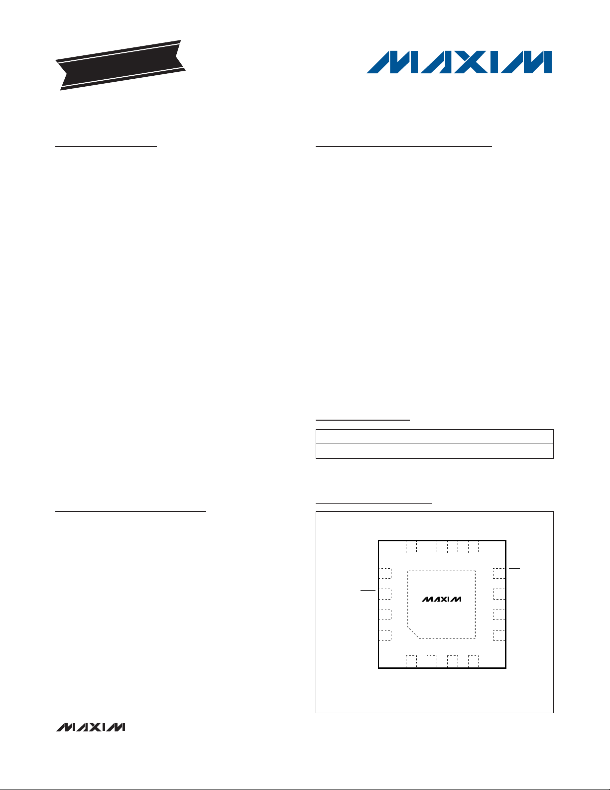
Pin Configuration
Ordering Information
19-4299; Rev 1; 3/09
For pricing, delivery, and ordering information, please contact Maxim Direct at 1-888-629-4642,
or visit Maxim’s website at www.maxim-ic.com.
EVALUATION KIT
AVAILABLE
PART TEMP RANGE
PIN-PACKAGE
MAX15031ATE+
-40°C to +125°C 16 TQFN-EP*
+
Denotes a lead(Pb)-free/RoHS-compliant package.
*
EP = Exposed pad.
Typical Operating Circuits appear at end of data sheet.
TOP VIEW
BIAS
13
14
SHDN
PGND
15
16
LX
*EXPOSED PAD
APD
12 11 9
+
12
PWR
(4mm
CLAMP
MAX15031
CP
THIN QFN
× 4mm)
10
3
CN MOUT
*EP
4
RLIM
IN
ILIM
8
7
CNTRL
FB
6
SGND
5
Page 2
MAX15031
80V, 300mW Boost Converter and Current
Monitor for APD Bias Applications
2 _______________________________________________________________________________________
ABSOLUTE MAXIMUM RATINGS
ELECTRICAL CHARACTERISTICS
(VIN= V
PWR
= 3.3V. V
SHDN
= 3.3V. CIN= C
PWR
= 10µF. CCP= 10nF, V
CNTRL
= VIN. V
RLIM
= 0. V
PGND
= V
SGND
= 0. V
BIAS
= 40V.
APD = unconnected. CLAMP = unconnected. ILIM = unconnected, MOUT = unconnected. T
A
= TJ= -40°C to +125°C, unless other-
wise noted. Typical values are at T
A
= +25°C.) (Note 2)
Stresses beyond those listed under “Absolute Maximum Ratings” may cause permanent damage to the device. These are stress ratings only, and functional
operation of the device at these or any other conditions beyond those indicated in the operational sections of the specifications is not implied. Exposure to
absolute maximum rating conditions for extended periods may affect device reliability.
Note 1: Package thermal resistances were obtained using the method described in JEDEC specification JESD51-7, using a four-
layer board. For detailed information on package thermal considerations, refer to www.maxim-ic.com/thermal-tutorial
.
PWR, IN to SGND ...................................................-0.3V to +12V
LX to PGND ............................................................-0.3V to +80V
BIAS, APD to SGND ...............................................-0.3V to +80V
SHDN to SGND............................................-0.3V to (V
IN
+ 0.3V)
CLAMP to SGND......................................-0.3V to (V
BIAS
+ 0.3V)
FB, ILIM, RLIM, CP, CN, CNTRL to SGND .............-0.3V to +12V
PGND to SGND .....................................................-0.3V to +0.3V
MOUT to SGND ....................................-0.3V to (V
CLAMP
+ 0.3V)
Continuous Power Dissipation
16-Pin TQFN (derate 25mW/°C above +70°C) ............2000mW
Thermal Resistance (Note 1)
θ
JA
....................................................................................40°C/W
θ
JC
......................................................................................6°C/W
Operating Temperature Range .........................-40°C to +125°C
Junction Temperature......................................................+150°C
Storage Temperature Range .............................-65°C to +150°C
Lead Temperature (soldering, 10s) .................................+300°C
Supply Voltage Range VIN, V
Supply Current I
Undervoltage Lockout Threshold V
Undervoltage Lockout Hysteresis V
Shutdown Current I
Shutdown Input Bias Current I
BOOST CONVERTER
Output-Voltage Adjustment
Range
Switching Frequency f
Maximum Duty Cycle D
FB Set-Point Voltage V
FB Input Bias Current I
Internal Switch On-Resistance R
Peak Switch Current Limit I
LX Leakage Current VLX = 36V 1 µA
Line Regulation
Load Regulation 0 ≤ I
PARAMETER SYMBOL CONDITIONS MIN TYP MAX UNITS
PWR
CP connected to IN, CCP = open 5.5 11
VFB = 1.4V, no switching 1 2
SUPPLY
UVLO
UVLO_HYS
IN_SHDN
BIAS_SHDNVBIAS
SW
CLK
FB
FB
VIN = 11V, VFB = 1.4V (no switching),
C
= open, CP = IN
CP
VIN rising 2.375 2.5 2.675 V
SHDN pulled low 2 µA
= 3.3V, V
VIN = V
PWR
2.9V ≤ V
2.9V ≤ V
PWR
PWR
ILX = 100mA
ON
ILX = 100mA,
= V
V
CP
IN V
LIM_LX
2.9V ≤ V
I
LOAD
PWR
= 4.5mA
≤ 4.5mA 1 %
LOAD
2.7 5.5
1.2 3
100 mV
= 0 30 µA
SHDN
VIN +
1V
76 V
= 5V 360 400 440
≤ 11V, V
≤ 11V, VIN = V
= V
IN
PWR
PWR
352 400 448
86 90 94 %
1.2201 1.245 1.2699 V
100 nA
V
= VIN = 2.9V,
PWR
V
= 5.5V
CP
= VIN = 5.5V,
V
PWR
= 10V
V
CP
V
= VIN = VCP = 5.5V 1 2
PWR
= VIN = VCP = 11V 1 2
PWR
12
12
0.8 1.2 1.6 A
≤ 11V, V
PWR
= VIN,
0.2 %
V
mA
kHz
Ω
Page 3
MAX15031
80V, 300mW Boost Converter and Current
Monitor for APD Bias Applications
_______________________________________________________________________________________ 3
Note 2: All minimum/maximum parameters are tested at TA= +125°C. Limits over temperature are guaranteed by design.
Note 3: Guaranteed by design and not production tested.
ELECTRICAL CHARACTERISTICS (continued)
(VIN= V
PWR
= 3.3V. V
SHDN
= 3.3V. CIN= C
PWR
= 10µF. CCP= 10nF, V
CNTRL
= VIN. V
RLIM
= 0. V
PGND
= V
SGND
= 0. V
BIAS
= 40V.
APD = unconnected. CLAMP = unconnected. ILIM = unconnected, MOUT = unconnected. T
A
= TJ= -40°C to +125°C, unless other-
wise noted. Typical values are at T
A
= +25°C.) (Note 2)
PARAMETER SYMBOL CONDITIONS MIN TYP MAX UNITS
Soft-Start Duration 8ms
Soft-Start Steps (0.25 x I
LIM_LX
) to I
LIM_LX
32 Steps
CONTROL INPUT (CNTRL)
Maximum Control Input Voltage
Range
FB set point is regulated to V
CNTRL
1.25 V
CURRENT MONITOR
Bias Voltage Range V
Bias Quiescent Current I
Voltage Drop V
Dynamic Output Resistance at
MOUT
BIAS
BIAS
DROPIAPD
R
MOUT
I
= 500nA 100 µA
APD
I
= 2mA 3.2 mA
APD
= 2mA, V
I
= 500nA 1 GΩ
APD
I
= 2.5mA 890 MΩ
APD
DROP
= V
BIAS
- V
APD
10 76 V
1V
MOUT Output Leakage APD is unconnected 1 nA
V
-
Output Clamp Voltage
Output Clamp Leakage Current V
Output-Voltage Range V
Current Gain I
Power-Supply Rejection Ratio PSRR
APD Input Current Limit I
Current-Limit Adjustment Range 12.45kΩ ≥ R
Power-Up Settling Time t
MOUT
V
CLAMP
MOUT
MOUT/IAPD
Forward diode current = 1mA 0.5 0.73 0.95 V
10V ≤ V
is unconnected
I
APD
I
APD
(∆I
V
LIM_APDVAPD
I
MOUT
0.1%, 10nF connected
S
from APD to ground
BIAS
= V
BIAS
= 76V 1 nA
CLAMP
≤ 76V, 0 ≤ I
≤ 1mA, CLAMP
APD
V
BIAS
-
1V
= 500nA 0.095 0.1 0.11
= 2mA 0.965 0.1 0.1035
I
= 500nA
MOUT/IMOUT
= 10V to 76V
BIAS
= 35V, R
settles to within
APD
BIAS
,
(Note 3)
= 5µA to
I
APD
)/∆V
1mA
= 3.3kΩ 3.15 3.75 4.35 mA
LIM
≥ 2.5kΩ 15mA
LIM
I
= 500nA 7.5 ms
APD
I
= 2.5mA 90 µs
APD
-1000 +300 +1500
-250 +24 +250
V
ppm/V
LOGIC INPUTS/OUTPUTS
SHDN Input-Voltage Low V
SHDN Input-Voltage High V
ILIM Output-Voltage Low V
ILIM Output Leakage Current I
OL
OH
IL
IH
I
= 2mA 0.3 V
LIM
V
= 11V 1 µA
ILIM
2.4 V
0.8 V
THERMAL PROTECTION
Thermal Shutdown Temperature rising +160 °C
Thermal Shutdown Hysteresis 10 °C
Page 4
MAX15031
80V, 300mW Boost Converter and Current
Monitor for APD Bias Applications
4 _______________________________________________________________________________________
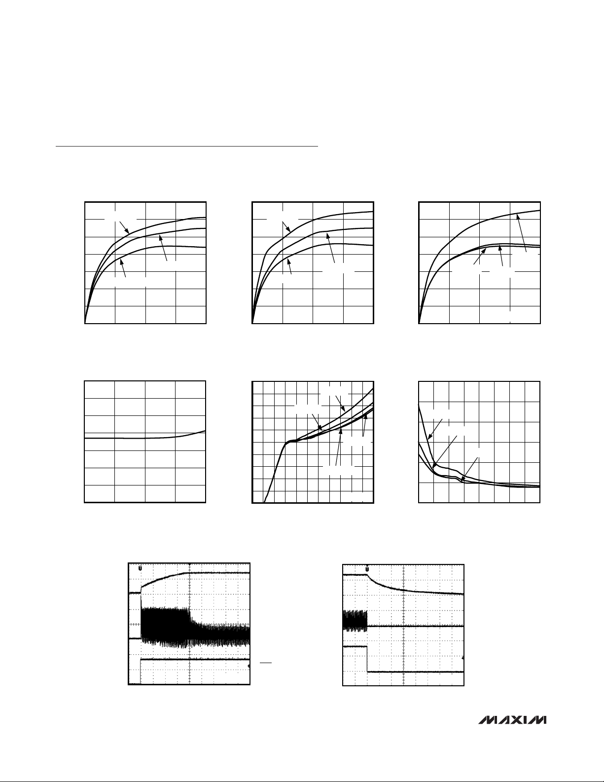
Typical Operating Characteristics
(V
PWR
= VIN= 3.3V, V
OUT
= 70V, circuit of Figure 3 (Figure 4 for VIN> 5.5V), unless otherwise noted.)
EFFICIENCY vs. LOAD CURRENT
MAX15031 toc01
LOAD CURRENT (mA)
EFFICIENCY (%)
321
10
20
30
40
50
60
70
0
04
V
OUT
= 30V
V
OUT
= 55V
V
OUT
= 70V
V
IN
= 3.3V
EFFICIENCY vs. LOAD CURRENT
MAX15031 toc02
LOAD CURRENT (mA)
EFFICIENCY (%)
321
10
20
30
40
50
60
70
0
04
V
OUT
= 30V
V
OUT
= 55V
V
OUT
= 70V
V
IN
= 5V
EFFICIENCY vs. LOAD CURRENT
MAX15031 toc03
LOAD CURRENT (mA)
EFFICIENCY (%)
321
10
20
30
40
50
60
70
0
04
VIN = 3.3V
VIN = 5V
VIN = 8V
V
OUT
= 70V
MINIMUM STARTUP VOLTAGE
vs. LOAD CURRENT
MAX15031 toc04
LOAD CURRENT (mA)
MINIMUM STARTUP VOLTAGE (V)
321
2.49
2.50
2.51
2.52
2.53
2.54
2.55
2.48
04
SUPPLY CURRENT
vs. SUPPLY VOLTAGE
MAX15031 toc05
SUPPLY VOLTAGE (V)
SUPPLY CURRENT (mA)
1097 82 3 4 5 61
0.2
0.4
0.6
0.8
1.0
1.2
1.4
1.6
1.8
2.0
0
011
VFB = 1.4V
TA = +125°C
TA = +85°C
TA = -40°C
TA = +25°C
NO-LOAD SUPPLY CURRENT
vs. SUPPLY VOLTAGE
XMAX15031 toc06
SUPPLY VOLTAGE (V)
NO-LOAD SUPPLY CURRENT (mA)
10987654
10
20
30
40
50
60
0
311
TA = +85°C
TA = -40°C
TA = +25°C
EXITING SHUTDOWN
MAX15031 toc07
1ms/div
V
OUT
50V/div
I
L
500mA/div
V
SHDN
2V/div
3V
0V
0mA
I
OUT
= 1mA
ENTERING SHUTDOWN
MAX15031 toc08
4ms/div
OUTPUT VOLTAGE
50V/div
INDUCTOR CURRENT
500mA/div
SHUTDOWN VOLTAGE
2V/div
3V
70V
0V
0mA
I
LOAD
= 1mA
Page 5
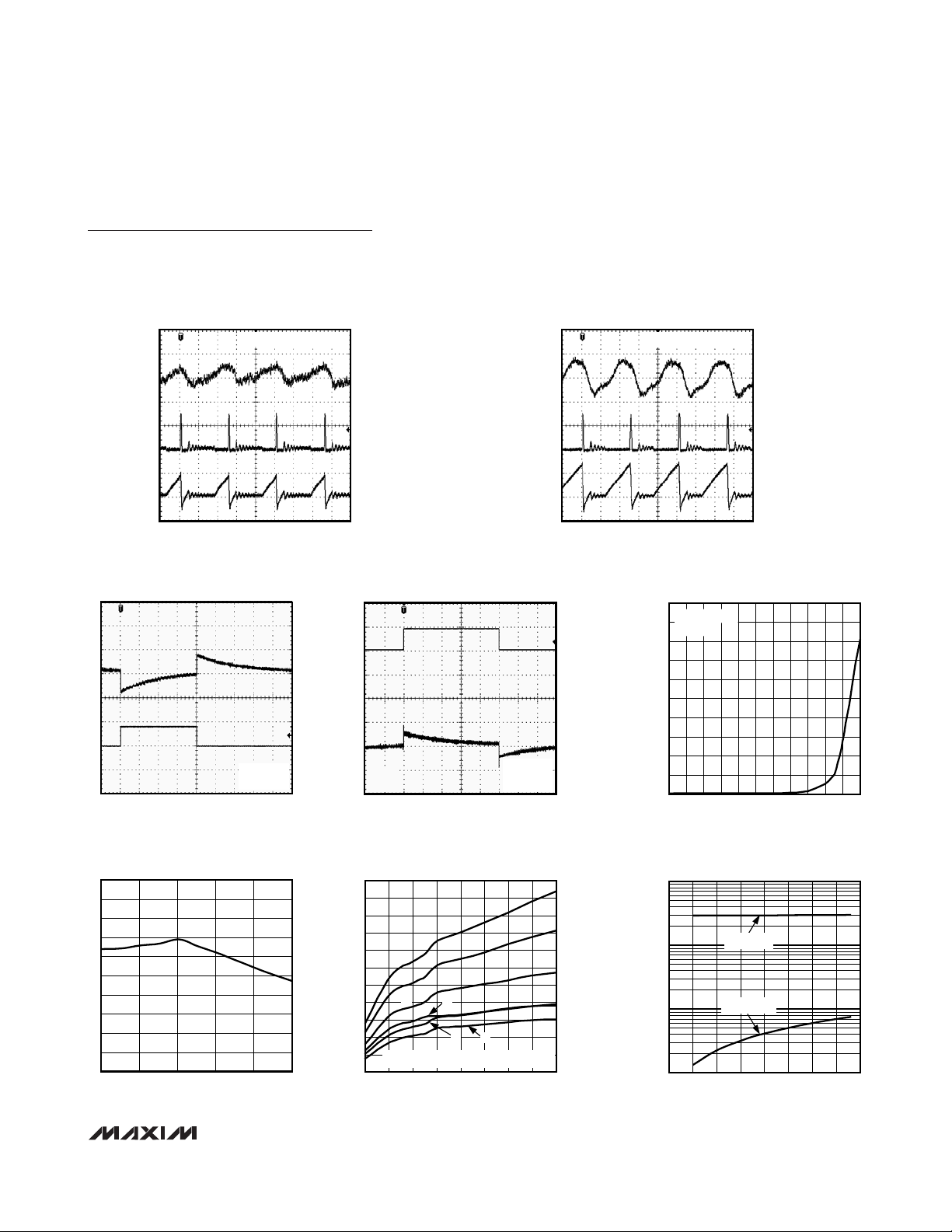
LIGHT-LOAD SWITCHING
WAVEFORM WITH RC FILTER
MAX15031 toc09
1µs/div
V
BIAS
AC-COUPLED
V
LX
50V/div
I
L
500mA/div
1mV/div
0mA
0V
I
OUT
= 0.1mA, V
BIAS
= 70V
MAX15031
80V, 300mW Boost Converter and Current
Monitor for APD Bias Applications
_______________________________________________________________________________________ 5
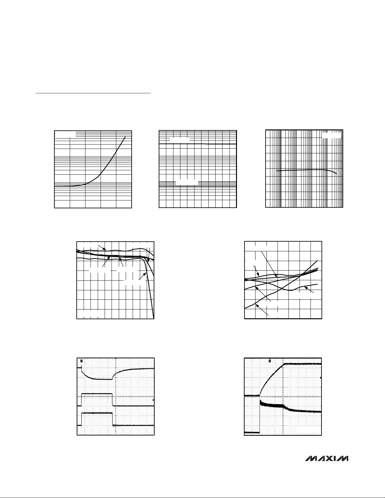
Typical Operating Characteristics (continued)
(V
PWR
= VIN= 3.3V, V
OUT
= 70V, circuit of Figure 3 (Figure 4 for VIN> 5.5V), unless otherwise noted.)
MAXIMUM LOAD CURRENT
vs. INPUT VOLTAGE
MAX15031 toc15
INPUT VOLTAGE (V)
MAXIMUM LOAD CURRENT (mA)
1097 85 64
10
20
30
40
50
60
70
80
90
100
110
0
311
A
B
C
A: V
OUT
= 30V, B: V
OUT
= 35V, C: V
OUT
= 45V,
D: V
OUT
= 55V, E: V
OUT
= 60V, F: V
OUT
= 72V
D
E
F
LOAD REGULATION
MAX15031 toc14
LOAD CURRENT (mA)
OUTPUT VOLTAGE (V)
4321
68.2
68.4
68.6
68.8
69.0
69.2
69.4
69.6
69.8
70.0
68.0
05
BIAS CURRENT
vs. BIAS VOLTAGE
MAX15031 toc16
BIAS VOLTAGE (V)
BIAS CURRENT (mA)
70605040302010
0.1
1
10
0.01
080
I
APD
= 2mA
I
APD
= 500nA
LOAD-TRANSIENT RESPONSE
100ms/div
HEAVY-LOAD SWITCHING
WAVEFORM WITH RC FILTER
MAX15031 toc11
V
OUT
= 3.3V
V
IN
= 70V
V
OUT
AC-COUPLED
200mV/div
I
LOAD
5mA/div
0mA
LINE-TRANSIENT RESPONSE
100ms/div
MAX15031 toc12
V
OUT
I
OUT
t
RISE
= 70V
= 1mA
= 50µs
V
IN
2V/div
3.3V
V
OUT
AC-COUPLED
100mV/div
MAX15031 toc10
I
OUT
1µs/div
= 4mA, V
BIAS
= 70V
V
BIAS
AC-COUPLED
1mV/div
V
LX
50V/div
0V
I
L
500mA/div
0mA
LX LEAKAGE CURRENT
vs. TEMPERATURE
200
CURRENT INTO
180
LX PIN
160
140
120
100
80
60
LX LEAKAGE CURRENT (nA)
40
20
0
-40 125
TEMPERATURE (°C)
MAX15031 toc13
1109565 80-10 5 20 35 50-25
Page 6
MAX15031
80V, 300mW Boost Converter and Current
Monitor for APD Bias Applications
6 _______________________________________________________________________________________
Typical Operating Characteristics (continued)
(V
PWR
= VIN= 3.3V, V
OUT
= 70V, circuit of Figure 3 (Figure 4 for VIN> 5.5V), unless otherwise noted.)
BIAS CURRENT
vs. APD CURRENT
MAX15031 toc17
APD CURRENT (mA)
BIAS CURRENT (mA)
10.10.010.001
0.1
1
10
0.01
0.0001 10
V
BIAS
= 70V
BIAS CURRENT
vs. TEMPERATURE
MAX15031 toc18
TEMPERATURE (°C)
BIAS CURRENT (mA)
1109580655035205-10-25
0.1
1
10
0.01
-40 125
I
APD
= 2mA
I
APD
= 500nA
GAIN ERROR
vs. APD CURRENT
MAX15031 toc19
I
APD
(µA)
GAIN ERROR (%)
1000100101
-4
-3
-2
-1
0
1
2
3
4
5
-5
0.1 10,000
V
BIAS
= 70V
GAIN ERROR
vs. TEMPERATURE
MAX15031 toc20
TEMPERATURE (°C)
GAIN ERROR (%)
11095-25 -10 5 35 50 6520 80
-2.5
-2.0
-1.5
-1.0
-0.5
0
0.5
1.0
-3.0
-40 125
V
BIAS
= 70V
I
APD
= 500nA
I
APD
= 50µA
I
APD
= 5µA
I
APD
= 2mA
I
APD
= 500µA
GAIN ERROR
vs. BIAS VOLTAGE
MAX15031 toc21
BIAS VOLTAGE (V)
GAIN ERROR (%)
706020 30 40 50
-0.60
-0.40
-0.20
0
0.20
0.40
0.60
0.80
-0.80
10 80
I
APD
= 500nA
I
APD
= 50µA
I
APD
= 5µA
I
APD
= 2mA
I
APD
= 500µA
APD TRANSIENT RESPONSE
MAX15031 toc22
20µs/div
V
APD
AC-COUPLED
70V
2V/div
I
APD
2.5mA/div
I
MOUT
0.25mA/div
0mA
0mA
STARTUP DELAY
MAX15031 toc23
200µs/div
V
BIAS
20V/div
I
MOUT
20nA/div
3V
0nA
I
APD
= 500nA
Page 7

MAX15031
80V, 300mW Boost Converter and Current
Monitor for APD Bias Applications
_______________________________________________________________________________________ 7
Typical Operating Characteristics (continued)
(V
PWR
= VIN= 3.3V, V
OUT
= 70V, circuit of Figure 3 (Figure 4 for VIN> 5.5V), unless otherwise noted.)
VOLTAGE DROP
vs. APD CURRENT
MAX15031 toc28
I
APD
(µA)
V
BIAS
- V
APD
(V)
1000100101
0.20
0.40
0.60
0.80
1.00
1.20
1.40
0
0.1 10,000
TA = +25°C
TA = -40°C
TA = +125°C
TA = +85°C
SWITCHING FREQUENCY
vs. TEMPERATURE
MAX15031 toc29
TEMPERATURE (°C)
SWITCHING FREQUENCY (kHz)
1109565 80-10 5 20 35 50-25
320
340
360
380
400
420
440
460
480
500
300
-40 125
STARTUP DELAY
100µs/div
STARTUP DELAY
MAX15031 toc24
I
APD
MAX15031 toc26
= 2mA
V
APD
20V/div
3V
I
MOUT
50µA/div
0nA
V
BIAS
2V/div
SHORT-CIRCUIT RESPONSE
STARTUP DELAY
100µs/div
I
V
APD
BIAS
MAX15031 toc25
= 500nA
= 5V
MAX15031 toc27
V
APD
2V/div
0V
I
MOUT
20nA/div
0nA
I
LIM
2V/div
0V
40µs/div
I
V
APD
BIAS
= 2mA
= 5V
0V
I
MOUT
50µA/div
0nA
40ms/div
V
BIAS
T
A
R
LIM
= 70V
= +85°C
= 2kΩ
I
BIAS
2mA/div
0mA
Page 8

MAX15031
80V, 300mW Boost Converter and Current
Monitor for APD Bias Applications
8 _______________________________________________________________________________________
Typical Operating Characteristics (continued)
(V
PWR
= VIN= 3.3V, V
OUT
= 70V, circuit of Figure 3 (Figure 4 for VIN> 5.5V), unless otherwise noted.)
SWITCHING FREQUENCY
vs. INPUT VOLTAGE
500
480
460
440
420
400
380
360
SWITCHING FREQUENCY (kHz)
340
320
300
212
INPUT VOLTAGE (V)
FB SET-POINT VARIATION
vs. TEMPERATURE
1.277
VIN = 2.9V
1.257
1.247
1.237
1.227
VIN = 5.5V
VIN = 2.9V
VIN = 5.5V
10864
FB RISING
FB FALLING
MAX15031 toc30
MAX15031 toc32
SWITCHING FREQUENCY AND
DUTY CYCLE vs. LOAD CURRENT
420
415
410
405
400
395
390
SWITCHING FREQUENCY (kHz)
385
380
04
SWITCHING FREQUENCY
LOAD CURRENT (mA)
APD OUTPUT RIPPLE VOLTAGE
MAX15031 toc31
DUTY CYCLE
MEASURED AT CN
321
MAX15031 toc33
60
50
40
DUTY CYCLE
30
20
10
0
V
APD
AC-COUPLED, 55V
200µV/div
1.217
FB SET-POINT VOLTAGE VARIATION (V)
1.207
-40 125
TEMPERATURE (°C)
APD OUTPUT RIPPLE VOLTAGE
0.1µF CAPACITOR CONNECTED
FROM APD TO GND.
2µs/div
1109580655035205-10-25
MAX15031 toc34
V
APD
AC-COUPLED, 55V
100µV/div
2µs/div
APD OUTPUT RIPPLE VOLTAGE
0.1µF CAPACITOR CONNECTED
FROM APD TO GND.
2µs/div
MAX15031 toc35
V
APD
AC-COUPLED, 70V
500µV/div
Page 9

MAX15031
80V, 300mW Boost Converter and Current
Monitor for APD Bias Applications
_______________________________________________________________________________________ 9
Pin Description
PIN NAME FUNCTION
1 PWR
2CP
3CN
4IN
5 SGND
6FB
7 CNTRL
8 ILIM Open-Drain Current-Limit Indicator. ILIM asserts low when the APD current limit has been exceeded.
9 RLIM
10 MOUT Current-Monitor Output. MOUT sources a current 1/10th of I
11 CLAMP Clamp Voltage Input. CLAMP is the external potential used for voltage clamping of MOUT.
12 APD Reference Current Output. APD provides the source current to the cathode of the photodiode.
13 BIAS
14 SHDN
15 PGND
16 LX
—EP
Boost Converter Input Voltage. PWR powers the switch driver and charge pump. Bypass PWR to PGND with a
ceramic capacitor of 1µF minimum value.
Positive Terminal of the Charge-Pump Flying Capacitor for 2.7V to 5.5V Supply Voltage Operation. Connect
CP to IN when the input voltage is in the 5.5V to 11V range.
Negative Terminal of the Charge-Pump Flying Capacitor for 2.7V to 5.5V Supply Voltage Operation. Leave CN
unconnected when the input voltage is in the 5.5V to 11V range.
Input Supply Voltage. IN powers all blocks of the MAX15031 except the switch driver and charge pump.
Bypass IN to PGND with a ceramic capacitor of 1µF minimum value.
Signal Ground. Connect directly to the local ground plane. Connect SGND to PGND at a single point, typically
near the return terminal of the output capacitor.
Feedback Regulation Input. Connect FB to the center tap of a resistive voltage-divider from the output (V
to SGND to set the output voltage. The FB voltage regulates to 1.245V (typ) when V
and to V
Control Input for Boost Converter Output-Voltage Programmability. Allows the feedback set-point voltage to be
set externally by CNTRL when CNTRL is less than 1.245V. Pull CNTRL above 1.5V (typ) to use the internal
1.245V (typ) feedback set-point voltage.
Current-Limit Resistor Connection. Connect a resistor from RLIM to SGND to program the APD current-limit
threshold.
Bias Voltage Input. Connect BIAS to the boost converter output (V
filter for ripple attenuation. BIAS provides the voltage bias for the current monitor and is the current source for
APD.
Active-Low Shutdown Control Input. Apply a logic-low voltage to SHDN to shut down the device and reduce
the supply current to 2µA (max). Connect SHDN to IN for normal operation. Ensure that V
than the input voltage, V
Power Ground. Connect the negative terminals of the input and output capacitors to PGND. Connect PGND
externally to SGND at a single point, typically at the return terminal of the output capacitor.
Drain of Internal 80V n-Channel DMOS. Connect inductor and diode to LX. Minimize the trace area at LX to
reduce switching noise emission.
Exposed Pad. Connect EP to a large contiguous copper plane at SGND potential to improve thermal
dissipation. Do not use as the main SGND connection.
voltage when V
CNTRL
.
IN
is below 1.245V (typ).
CNTRL
APD
.
) either directly or through a lowpass
OUT
is above 1.5V (typ)
CNTRL
is not greater
SHDN
OUT
)
Page 10

MAX15031
80V, 300mW Boost Converter and Current
Monitor for APD Bias Applications
10 ______________________________________________________________________________________
Functional Diagram
Detailed Description
The MAX15031 constant-frequency, current-mode, PWM
boost converter is intended for low-voltage systems that
require a locally generated high voltage. This device can
generate a low-noise, high output voltage required for
PIN and varactor diode biasing and LCD displays. The
MAX15031 operates either from +2.7V to +5.5V or from
+5.5V to +11V. For 2.7V to 5.5V operation, an internal
charge pump with an external 10nF ceramic capacitor is
used. For 5.5V to 11V operation, connect CP to IN and
leave CN unconnected.
The MAX15031 operates in discontinuous mode in
order to reduce the switching noise caused by reversevoltage recovery charge of the rectifier diode. Other
continuous mode boost converters generate large voltage spikes at the output when the LX switch turns on
because there is a conduction path between the output, diode, and switch to ground during the time needed for the diode to turn off and reverse its bias voltage.
To reduce the output noise even further, the LX switch
turns off by taking 10ns typically to transition from ON
to OFF. As a consequence, the positive slew rate of the
LX node is reduced and the current from the inductor
does not “force” the output voltage as hard as would
be the case if the LX switch were to turn off faster.
The constant-frequency (400kHz) PWM architecture
generates an output voltage ripple that is easy to filter.
An 80V vertical DMOS device used as the internal
power switch is ideal for boost converters with output
voltages up to 76V. The MAX15031 can also be used in
other topologies where the PWM switch is grounded,
like SEPIC and flyback converters.
PWR
OUTPUT ERROR AND CURRENT
FB
CNTRL
SGND
V
REF
V
REF
MUX
REFERENCE
COMPARATOR
COMPARATOR
-A
+A
-C
+C
SOFTSTART
PEAK CURRENT-LIMIT
COMPARATOR
SWITCH
CONTROL
LOGIC
80V
DMOS
CURRENT
LX
PGND
SWITCH
SENSE
CN
CP
IN
CHARGE
PUMP
(DOUBLER)
UVLO
THERMAL
SHUTDOWN
MAX15031
BIAS AND
REFERENCE
CLK
OSCILLATOR
400kHz
SHDN BIAS
1x
V
REF
CURRENT
MONITOR
10x
CURRENT-
LIMIT
ADJUSTMENT
CURRENT
LIMIT
CLAMP
MOUT
RLIM
APD
ILIM
Page 11

MAX15031
The MAX15031 includes a versatile current monitor
intended for monitoring the APD, PIN, or varactor diode
DC current in fiber and other applications. The
MAX15031 features more than three decades of
dynamic current ranging from 500nA to 4mA and provides an output current accurately proportional to the
APD current at MOUT.
The MAX15031 also features a shutdown logic input to
disable the device and reduce its standby current to
2µA (max).
Fixed-Frequency PWM Controller
The heart of the MAX15031 current-mode PWM controller is a BiCMOS multiple-input comparator that
simultaneously processes the output-error signal and
switch current signal. The main PWM comparator uses
direct summing, lacking a traditional error amplifier and
its associated phase shift. The direct summing configuration approaches ideal cycle-by-cycle control over the
output voltage since there is no conventional error
amplifier in the feedback path.
The device operates in PWM mode using a fixed-frequency, current-mode operation. The current-mode frequency loop regulates the peak inductor current as a
function of the output error signal.
The current-mode PWM controller is intended for DCM
(discontinuous conduction mode) operation. No internal
slope compensation is added to the current signal.
Charge Pump
At low supply voltages (2.7V to 5.5V), internal chargepump circuitry and an external 10nF ceramic capacitor
connected between CP and CN double the available internal supply voltage to drive the internal switch efficiently.
In the 5.5V to 11V supply voltage range, the charge
pump is not required. In this configuration, disable the
charge pump by connecting CP to IN and leaving CN
unconnected.
Monitor Current Limit (RLIM)
The current limit of the current monitor is programmable
from 1mA to 5mA. Connect a resistor from RLIM to
ground to program the current-limit threshold up to 5mA.
The current monitor mirrors the current out of APD with
a 1:10 ratio, and the MOUT current can be converted to
a voltage signal by connecting a resistor from MOUT to
SGND.
The APD current-monitor range is from 500nA to 4mA,
and the MOUT current-mirror output accuracy is ±10%
from 500nA to 1mA of APD current and ±3.5% from
1mA to 4mA of APD current.
Clamping the Monitor
Output Voltage (CLAMP)
CLAMP provides a means for diode clamping the voltage at MOUT; thus V
MOUT
is limited to (V
CLAMP
+
0.6V). CLAMP can be connected to either an external
supply or BIAS. CLAMP can be left unconnected if voltage clamping is not required.
Adjusting the Boost Converter
Output Voltage (FB/CNTRL)
The boost converter output voltage can be set by connecting FB to a resistor-divider from V
OUT
to ground.
The set-point feedback reference is the 1.245 (typ)
internal reference voltage when V
CNTRL
> 1.5V and is
equal to the CNTRL voltage when V
CNTRL
< 1.25V.
To change the converter output on the fly, apply a voltage lower than 1.25V (typ) to the CNTRL input and
adjust the CNTRL voltage, which is the reference input
of the error amplifier when V
CNTRL
< 1.25V (see the
Functional Diagram
). This feature can be used to adjust
the APD voltage based on the APD mirror current,
which compensates for the APD avalanche gain variation with temperature and manufacturing process. As
shown in Figure 4, the voltage signal proportional to the
MOUT current is connected to the ADC (analog to digital) input of the APD module, which then controls the
reference voltage of the boost converter error amplifier
through a DAC (digital to analog) block connected to
the CNTRL input. The BIAS voltage and, therefore, the
APD current, are controlled based on the MOUT mirror
current, forming a negative feedback loop.
Shutdown (
SHDN
)
The MAX15031 features an active-low shutdown input
(SHDN). Pull SHDN low to enter shutdown. During shut-
down, the supply current drops to 2µA (30µA from
BIAS) (max). However, the output remains connected to
the input through the inductor and the output diode,
holding the output voltage to one diode drop below
PWR when the MAX15031 shuts down. Connect SHDN
to IN for always-on operation.
80V, 300mW Boost Converter and Current
Monitor for APD Bias Applications
______________________________________________________________________________________ 11
Page 12

MAX15031
80V, 300mW Boost Converter and Current
Monitor for APD Bias Applications
12 ______________________________________________________________________________________
Design Procedure
Setting the Output Voltage
Set the MAX15031 output voltage by connecting a resistive divider from the output to FB to SGND (Figure 1).
Select R1(FB to SGND resistor) between 200kΩ and
400kΩ. Calculate R2(V
OUT
to FB resistor) using the fol-
lowing equation:
where V
OUT
can range from (VIN+ 1V) to 76V and V
REF
= 1.245V or V
CNTRL
depending on the V
CNTRL
value.
For V
CNTRL
> 1.5V, the internal 1.245V (typ) reference
voltage is used as the feedback set point (V
REF
=
1.245V) and for V
CNTRL
< 1.25V, V
REF
= V
CNTRL
.
Determining Peak Inductor Current
If the boost converter remains in the discontinuous
mode of operation, then the approximate peak inductor
current, I
LPEAK
(in amperes), is represented by the for-
mula below:
where TSis the switching period in microseconds,
V
OUT
is the output voltage in volts, V
IN_MIN
is the mini-
mum input voltage in volts, I
OUT_MAX
is the maximum
output current in amperes, L is the inductor value in
microhenrys, and η is the efficiency of the boost converter (see the
Typical Operating Characteristics
).
Determining the Inductor Value
Three key inductor parameters must be specified for
operation with the MAX15031: inductance value (L),
inductor saturation current (I
SAT
), and DC resistance
(DCR). In general, the inductor should have a saturation
current rating greater than the maximum switch peak
current-limit value (I
LIM-LX
= 1.6A). Choose an inductor
with a low-DCR resistance for reasonable efficiency.
Use the following formula to calculate the lower bound
of the inductor value at different output voltages and
output currents. This is the minimum inductance value
for discontinuous mode operation for supplying full
300mW of output power.
where V
IN_MIN
, V
OUT
(both in volts), and I
OUT
(in
amperes) are typical values (so that efficiency is optimum for typical conditions), TS(in microseconds) is the
period, η is the efficiency, and I
LIM_LX
is the peak
switch current in amperes (see the
Electrical
Characteristics
table).
Calculate the optimum value of L (L
OPTIMUM
) to ensure
the full output power without reaching the boundary
between continuous conduction mode (CCM) and DCM
using the following formula:
For a design in which VIN= 3.3V, V
OUT
= 70V, I
OUT
=
3mA, η = 45%, I
LIM-LX
= 1.3A, and TS= 2.5µs: L
MIN
=
1.3µH and L
MAX
= 23µH.
For a worse-case scenario in which VIN= 2.9V, V
OUT
=
70V, I
OUT
= 4mA, η = 43%, I
LIM-LX
= 1.3A, and TS=
2.5µs: L
MIN
= 1.8µH and L
MAX
= 15µH.
The choice of 4.7µH is reasonable given the worst-case
scenario above. In general, the higher the inductance,
the lower the switching noise. Load regulation is also
better with higher inductance.
Figure 1. Adjustable Output Voltage
V
OUT
R
2
FB
MAX15031
R
1
RR
21
⎡
⎛
V
=
OUT
⎢
⎜
V
⎝
REF
⎣
⎤
⎞
1
−
⎥
⎟
⎠
⎦
2T I (V V )
×× ×
S OUT OUT IN_MIN
L[H]
µη=
MIN
−
2
I
×
LIM-LX
L[H]
OPTIMUM
where L [ H]
MAX
µη=
2
V(VV)T
IN_MIN
L
MAX
µµ=
−
OUT IN_MIN S
×××IV
2
OUT
I
LPEAK
×× ×
=
S OUT IN_MIN OUT_MAX
−
L
×
η
2T (V V )I
[]
.H225
××
2
OUT
Page 13

MAX15031
Diode Selection
The MAX15031’s high switching frequency demands a
high-speed rectifier. Schottky diodes are recommended for most applications because of their fast recovery
time and low forward-voltage drop. Ensure that the
diode’s peak current rating is greater than the peak
inductor current. Also the diode reverse-breakdown
voltage must be greater than V
OUT
. The output voltage
of the boost converter.
Output Filter Capacitor Selection
For most applications, use a small output capacitor of
0.1µF or greater. To achieve low output ripple, a capacitor with low ESR, low ESL, and high capacitance value
should be selected. If tantalum or electrolytic capacitors
are used to achieve high capacitance values, always
add a smaller ceramic capacitor in parallel to bypass
the high-frequency components of the diode current.
The higher ESR and ESL of electrolytic capacitors
increase the output ripple and peak-to-peak transient
voltage. Assuming the contribution from the ESR and
capacitor discharge equals 50% (proportions may vary),
calculate the output capacitance and ESR required for a
specified ripple using the following equations:
For very low output ripple applications, the output of the
boost converter can be followed by an RC filter to further
reduce the ripple. Figure 2 shows a 100Ω (RF), 0.1µF
(CF) filter used to reduce the switching output ripple to
1mV
P-P
with a 0.1mA load or 2mV
P-P
with a 4mA load.
The output-voltage regulation resistor-divider must remain
connected to the diode and output capacitor node.
Use X7R ceramic capacitors for more stability over the full
temperature range. Use an X5R capacitor for -40°C to
+85°C applications.
Input Capacitor Selection
Bypass PWR to PGND with a 1µF (min) ceramic capacitor and bypass IN to PGND with a 1µF (min) ceramic
capacitor. Depending on the supply source impedance, higher values may be needed. Make sure that the
input capacitors are close enough to the IC to provide
adequate decoupling at IN and PWR as well. If the layout cannot achieve this, add another 0.1µF ceramic
capacitor between IN and PGND (or PWR and PGND)
in the immediate vicinity of the IC. Bulk aluminum electrolytic capacitors may be needed to avoid chattering
at low input voltage. In case of aluminum electrolytic
capacitors, calculate the capacitor value and ESR of
the input capacitor using the following equations:
OOU
Figure 2. Typical Operating Circuit with RC Filter
80V, 300mW Boost Converter and Current
Monitor for APD Bias Applications
______________________________________________________________________________________ 13
OUT
Ω
⎡
IxL
LPEAK OPTIM
T
⎢
S
⎢
⎣
0.5 x
∆V
=ESR m
I
(V V )−
OUT IN_MIN
OUT
T
I
C
[]µFV=−
OUT
0.5 x
OUT
∆
[]
UUM
⎤
⎥
⎥
⎦
VxI
C
[]µηFV=
IN
OUT OUT
xV x0.5x
IN_MIN IN
[]
⎡
TT
⎢
∆
⎢
⎣
0.5 xΩ∆ x η
VxV
=ESR m
VxI
OUT
IxL xV
LPEAK OPTIMUM OUT
−
S
V(VV
IN_MIN OUT I
IN IN_M
OUT
−
NN_MIN
IIN
)
⎤
⎥
⎥
⎦
VIN = 2.7V TO 5.5V V
C
PWR
C
CP
PWR
CNTRL
SHDN
CP
CN
PGND
IN
MAX15031
SGND
L1
C
IN
BIAS
R
F
LX
FB
D1
R
2
R
1
100Ω
C
OUT1
C
F
0.1µF
OUT
Page 14

MAX15031
80V, 300mW Boost Converter and Current
Monitor for APD Bias Applications
14 ______________________________________________________________________________________
Determining Monitor Current Limit
Calculate the value of the monitor current-limit resistor,
R
LIM
, for a given APD current limit, I
LIMIT
, using the fol-
lowing equation:
The R
LIM
resistor, R
LIM
, ranges from 12.45kΩ to 2.5Ω
for APD currents from 1mA to 5mA.
Applications Information
Using APD or PIN Photodiodes
in Fiber Applications
When using the MAX15031 to monitor APD or PIN photodiode currents in fiber applications, several issues
must be addressed. In applications where the photodiode must be fully depleted, keep track of voltages budgeted for each component with respect to the available
supply voltage(s). The current monitors require as
much as 1.1V between BIAS and APD, which must be
considered part of the overall voltage budget.
Additional voltage margin can be created if a negative
supply is used in place of a ground connection, as long
as the overall voltage drop experienced by the
MAX15031 is less than or equal to 76V. For this type of
application, the MAX15031 is suggested so the output
can be referenced to “true” ground and not the negative
supply. The MAX15031’s output current can be referenced as desired with either a resistor to ground or a
transimpedance amplifier. Take care to ensure that output voltage excursions do not interfere with the required
margin between BIAS and MOUT. In many fiber applications, MOUT is connected directly to an ADC that operates from a supply voltage that is less than the voltage
at BIAS. Connecting the MAX15031’s clamping diode
output, CLAMP, to the ADC power supply helps avoid
damage to the ADC. Without this protection, voltages
can develop at MOUT that might destroy the ADC. This
protection is less critical when MOUT is connected
directly to subsequent transimpedance amplifiers (linear
or logarithmic) that have low-impedance, near-groundreferenced inputs. If a transimpedance amplfier is used
on the low side of the photodiode, its voltage drop must
also be considered. Leakage from the clamping diode
is most often insignificant over nominal operating conditions, but grows with temperature.
To maintain low levels of wideband noise, lowpass filtering the output signal is suggested in applications where
only DC measurements are required. Connect the filter
capacitor at MOUT. Determining the required filtering
components is straightforward, as the MAX15031
exhibits a very high output impedance of 890MΩ.
In some applications where pilot tones are used to identify specific fiber channels, higher bandwidths are desired
at MOUT to detect these tones. Consider the minimum
and maximum currents to be detected, then consult the
frequency response and noise typical operating curves.
If the minimum current is too small, insufficient bandwidth
could result, while too high a current could result in
excessive noise across the desired bandwidth.
Layout Considerations
Careful PCB layout is critical to achieve low switching
losses and clean and stable operation. Protect sensitive
analog grounds by using a star ground configuration.
Connect SGND and PGND together close to the device
at the return terminal of the output bypass capacitor.
Do not connect them together anywhere else. Keep all
PCB traces as short as possible to reduce stray capacitance, trace resistance, and radiated noise. Ensure that
the feedback connection to FB is short and direct.
Route high-speed switching nodes away from the sensitive analog areas. Use an internal PCB layer for SGND
as an EMI shield to keep radiated noise away from the
device, feedback dividers, and analog bypass capacitors. Refer to the MAX15031 evaluation kit data sheet
for a layout example.
R10
=×
LIM
1.245V
I (mA)
LIMIT
Page 15

MAX15031
MAX15031
CNTRL
CP
CN
IN
PGND
FB
BIAS
SHDN
MOUTAPDSGNDRLIM
PWR
LX
GPIO
ILIM
GPIO
CLAMP
V
DD
µC
V
DD
APD
C
IN
1µF
C
CP
10nF
R
MOUT
10kΩ
C
OUT
0.1µF
C
MOUT
(OPTIONAL)
R
1
6.34kΩ
R
LIM
2.87kΩ
R
2
348kΩ
V
IN
C
PWR
1µF
L1
4.7µH
D1
V
OUT
(70V MAX)
DAC
ADC
R
F
100Ω
R
ADJ
C
F
0.1µF
Typical Operating Circuits
Figure 3. Typical Operating Circuit for VIN= 2.7V to 5.5V
80V, 300mW Boost Converter and Current
Monitor for APD Bias Applications
______________________________________________________________________________________ 15
Page 16

MAX15031
80V, 300mW Boost Converter and Current
Monitor for APD Bias Applications
16 ______________________________________________________________________________________
Typical Operating Circuits (continued)
Package Information
For the latest package outline information and land patterns, go
to www.maxim-ic.com/packages
.
PACKAGE TYPE PACKAGE CODE DOCUMENT NO.
16 TQFN T1644-4
21-0139
Chip Information
PROCESS: BiCMOS
Figure 4. Typical Operating Circuit for VIN= 5.5V to 11V
L1
= 5.5V TO 11V
V
IN
4.7µH
D1
V
OUT
(70V MAX)
C
IN
1µF
R
2.87kΩ
LIM
PWR
CNTRL
IN
CP
CN
C
1µF
MAX15031
PWR
APD
LX
PGND
BIAS
SHDN
ILIM
CLAMP
MOUTAPDSGNDRLIM
R
FB
MOUT
10kΩ
V
DD
C
OUT
0.1µF
C
MOUT
(OPTIONAL)
R
F
100Ω
C
F
0.1µF
GPIO
GPIO
V
DD
ADC
R
2
348kΩ
R
1
634kΩ
µC
DAC
Page 17

MAX15031
80V, 300mW Boost Converter and Current
Monitor for APD Bias Applications
Maxim cannot assume responsibility for use of any circuitry other than circuitry entirely embodied in a Maxim product. No circuit patent licenses are
implied. Maxim reserves the right to change the circuitry and specifications without notice at any time.
Maxim Integrated Products, 120 San Gabriel Drive, Sunnyvale, CA 94086 408-737-7600 ____________________
17
© 2009 Maxim Integrated Products Maxim is a registered trademark of Maxim Integrated Products, Inc.
Revision History
REVISION
NUMBER
0 10/08 Initial release —
1 3/09 Updated Electrical Characteristics and added new Note 3. 3
REVISION
DATE
DESCRIPTION
PAGES
CHANGED
 Loading...