

Page 1
General Description
The MAX15029/MAX15030 low-dropout linear regulators operate from input voltages as low as 1.425V and
deliver up to 500mA of continuous output current with a
typical dropout voltage of only 40mV. The output voltage is adjustable from 0.5V to VINand is ±2% accurate
over load and line variations, from -40°C to +125°C.
The MAX15030 features a BIAS input of 3V to 5.5V from
an always-on power supply. The BIAS input current is
reduced down to less than 2µA during the shutdown.
These regulators use small, 1µF ceramic input capacitors and 2.2µF ceramic output capacitors to deliver
500mA output current. High bandwidth provides excellent transient response and limits the output voltage deviation to 10mV for a 100mA to 500mA load step, with only
a 2.2µF ceramic output capacitor, and the voltage deviations can be reduced further by increasing the output
capacitor.
These devices offer a logic-controlled shutdown input
to reduce input current (I
IN
) consumption down to less
than 5.5µA in standby mode. Other features include a
soft-start to reduce inrush current, short-circuit protection, and thermal-overload protection.
The MAX15030 features a BIAS input allowing a secondary supply to keep the LDO’s internal circuitry alive
if the voltage on IN goes to 0. Both devices are fully
specified from -40°C to +125°C and are available in a
10-pin thermally enhanced TDFN package (3mm x
3mm) that includes an exposed pad for optimal power
dissipation. For a 1A version of these LDOs, refer to the
MAX15027/MAX15028 data sheet.
Applications
Automotive (Dead-Man LDO)
Servers
Storage
Networking
Base Stations
Optical Modules
ATE
Features
o 1.425V to 3.6V Input Voltage Range
o Output Voltage Programmable from 0.5V to V
IN
o Guaranteed Maximum 150mV Dropout at 500mA
Output Current
o 2% Output Accuracy Over Load, Line, and
Temperature
o Stable with Ceramic Capacitors
o Fast Transient Response
o 60µA Operating Bias Supply Current
o 1.2µA Shutdown Bias Supply Current
o Short-Circuit and Thermal Protection
o -40°C to +125°C Operating Temperature Range
o Soft-Start Limits Inrush Current
o Thermally Enhanced 3mm x 3mm TDFN Package
MAX15029/MAX15030
1.425V to 3.6V Input, 500mA Low-Dropout
Regulators with BIAS Input
________________________________________________________________
Maxim Integrated Products
1
Pin Configurations
Ordering Information
19-4586; Rev 0; 4/09
For pricing, delivery, and ordering information, please contact Maxim Direct at 1-888-629-4642,
or visit Maxim’s website at www.maxim-ic.com.
Pin Configurations continued at end of data sheet.
PART
TEMP RANGE
PIN-
TOP
MARK
MAX15029ATB+
+AUF
MAX15030ATB+
+AUG
+
Denotes a lead(Pb)-free/RoHS-compliant package.
For tape-and-reel orders, add a “T” after the “+.”
*
EP = Exposed pad.
Typical Operating Circuits appear at end of data sheet.
PACKAGE
- 40°C to + 125°C 10 TDFN-EP*
- 40°C to + 125°C 10 TDFN-EP*
TOP VIEW
+
IN
1
29
IN
3
I.C.
4
56
MAX15029
TDFN
(3mm x 3mm)
OUT
10
OUTIN
GND
8
FB
7
SSEN
Page 2
MAX15029/MAX15030
1.425V to 3.6V Input, 500mA Low-Dropout
Regulators with BIAS Input
2 _______________________________________________________________________________________
ABSOLUTE MAXIMUM RATINGS
ELECTRICAL CHARACTERISTICS
(Circuit of Figure 1; VIN= 1.8V, V
OUT
= 1.2V, EN = IN for MAX15029, EN = BIAS for MAX15030, I
OUT
= 100mA, T
A
=
T
J
= -40°C to
+125°C. Typical values are at T
A
= +25°C, unless otherwise noted.) (Note 2)
Stresses beyond those listed under “Absolute Maximum Ratings” may cause permanent damage to the device. These are stress ratings only, and functional
operation of the device at these or any other conditions beyond those indicated in the operational sections of the specifications is not implied. Exposure to
absolute maximum rating conditions for extended periods may affect device reliability.
IN, FB, SS, I.C. to GND..........................................-0.3V to +4.0V
BIAS to GND.............................................................-0.3V to +6V
EN to GND ................-0.3V to the lower of (V
BIAS
+ 0.3V) or +6V
OUT to GND ................................................-0.3V to (V
IN
+ 0.3V)
Output Short-Circuit Duration.....................................Continuous
Continuous Power Dissipation (T
A
= +70°C)
10-Pin TDFN, Multilayer Board
(derate 24.4mW/°C above +70°C)..............................1951mW
Junction-to-Case Thermal Resistance, θ
JC
(Note 1)..........9°C/W
Junction-to-Ambient Thermal Resistance, θ
JA
(Note 1)...41°C/W
Operating Junction Temperature Range...........-40°C to +125°C
Maximum Junction Temperature .....................................+150°C
Storage Temperature Range .............................-65°C to +150°C
Lead Temperature (soldering, 10s) .................................+300°C
Note 1: Package thermal resistances were obtained using the method described in JEDEC specification JESD51-7, using a four-
layer board. For detailed information on package thermal considerations, refer to www.maxim-ic.com/thermal-tutorial
.
PARAMETER SYMBOL CONDITIONS MIN TYP MAX UNITS
IN
Input Voltage Range V
Undervoltage Lockout V
Undervoltage Lockout Hysteresis V
Quiescent GND Current I
Input Supply Current in Shutdown I
BIAS (MAX15030)
Input Voltage Range V
Undervoltage Lockout V
Undervoltage Lockout Hysteresis I
Quiescent Input Supply Current I
Input Supply Current in Shutdown I
MAX15029 1.425 3.600
V
IN
UVLO
UVLO_HYSTIOUT
MAX15030
VIN rising
VIN = 1.425V to 3.6V, V
I
GND
OUT
VIN = 3.6V, V
VIN = 3.3V, V
IN_SD
BIAS
BIAS_UVLOVBIAS
BIAS
BIAS_SD
VEN = 0 (TA = -40°C to 85°C) 0.1 5.5 µA
OUT
VEN = V
EN = GND
= 2mA 50 mV
= 1mA, V
BIAS
OUT
OUT
= 3.3V, I
= 3.3V, I
rising 2.3 2.5 2.7 V
= 2mA 110 mV
BIAS
= 3V to 5.5V 1.425 3.600
BIAS
BIAS = IN 3.000 3.600
MAX15029 1.275 1.325 1.375
MAX15030 1.04 1.09 1.14
= 1.2V,
OUT
= 3.3V
= 100mA 180 325 560
OUT
= 500mA 170 315 470
OUT
VIN = 0, V
V
BIAS
V
I N
V
B I AS
V
I N
V
B I AS
OUT
= 3.3V
= 3.3V , V
= 3.3V
= 3.3V , V
= 5V
= 0,
OU T
OU T
= 0,
= 0,
160 275 410
3 5.5 V
20 60 120 µA
1.2 2
1.2 2
1.5 3
V
V
µA
µA
Page 3
MAX15029/MAX15030
1.425V to 3.6V Input, 500mA Low-Dropout
Regulators with BIAS Input
_______________________________________________________________________________________ 3
ELECTRICAL CHARACTERISTICS (continued)
(Circuit of Figure 1; VIN= 1.8V, V
OUT
= 1.2V, EN = IN for MAX15029, EN = BIAS for MAX15030, I
OUT
= 100mA, T
A
=
T
J
= -40°C to
+125°C. Typical values are at T
A
= +25°C, unless otherwise noted.) (Note 2)
Note 2: All devices are production tested at T
A
= +25°C. Limits over the operating temperature range are guaranteed by design
and characterization.
PARAMETER SYMBOL CONDITIONS MIN TYP MAX UNITS
OUT
Output Voltage Range V
Load Regulation I
Line Regulation
Dropout Voltage (VIN - V
(Note 3)
Output Current Limit I
FB
Threshold Accuracy V
Input Current I
EN/SOFT-START
Enable Input Threshold
(MAX15030)
Enable Input Threshold
(MAX15029)
Soft-Start Charging Current I
Soft-Start Reference Voltage V
THERMAL SHUTDOWN
Thermal Shutdown Threshold TJ rising 165 °C
Thermal Shutdown Hysteresis 15 °C
OUT
)
OUT
= 1mA to 500mA 0.01 mV/mA
OUT
V
V
LIM
V
V
V
V
DO
FB
FB
IH
IL
IH
IL
SS
SS
= 1.425V to 3.6V, V
IN
= 1mA
I
OUT
I
= 500mA, V
OUT
VFB = 300mV 0.7 0.85 1.0 A
= 1.125V to 3.3V, V
V
OUT
0.3V) to 3.6V, I
VFB = 0.488V 0.1 0.2 µA
V
= 5V
BIAS
VIN = 1.8V
OUT
= 1mA to 500mA
OUT
= 1.2V,
OUT
= 1.2V, V
= (V
IN
IN
0.5 3.3 V
4mV
= 1.5V 40 150 mV
+
OUT
0.489 0.499 0.509 V
1.05
1.05
5µA
0.499 V
0.4
0.4
V
V
Page 4

MAX15029/MAX15030
1.425V to 3.6V Input, 500mA Low-Dropout
Regulators with BIAS Input
4 _______________________________________________________________________________________
Typical Operating Characteristics
(Circuit of Figure 1, VIN= 1.8V, V
OUT
= 1.5V, I
OUT
= 500mA, TA= +25°C, unless otherwise noted.)
OUTPUT VOLTAGE
vs. INPUT VOLTAGE
MAX15029 toc01
OUTPUT VOLTAGE (V)
MAX15029 toc04
BIAS CURRENT (µA)
1.51
1.50
1.49
1.48
1.47
1.46
1.45
0 800
60
59
58
57
56
55
54
53
52
51
50
0 800
1.6
1.4
1.2
1.0
0.8
0.6
OUTPUT VOLTAGE (V)
0.4
I
= 0
0.2
0
04.0
INPUT VOLTAGE (V)
70
60
50
40
30
BIAS CURRENT (µA)
20
10
0
16
BIAS CURRENT
vs. BIAS VOLTAGE
BIAS VOLTAGE (V)
OUT
= 3.3V
V
BIAS
VIN = 1.8V
V
OUT
= 0
I
OUT
5432
3.53.00.5 1.0 1.5 2.0 2.5
= 1.5V
OUTPUT VOLTAGE
vs. OUTPUT CURRENT
OUTPUT CURRENT (mA)
BIAS CURRENT
vs. OUTPUT CURRENT
V
= 5.5V
BIAS
V
= 3.3V
BIAS
OUTPUT CURRENT (mA)
INPUT CURRENT
vs. INPUT VOLTAGE
MAX15029 toc02
INPUT CURRENT (mA)
1.4
1.2
1.0
0.8
0.6
0.4
0.2
0
04.0
INPUT VOLTAGE (V)
V
BIAS
= 0
I
OUT
MAX15029 toc03
= 3.3V
3.53.02.52.01.51.00.5
V
= 3.3V
BIAS
600400200
GROUND CURRENT
vs. OUTPUT CURRENT
1.4
1.2
MAX15029 toc05
1.0
0.8
0.6
0.4
GROUND CURRENT (mA)
0.2
0
600400200
0 500
OUTPUT CURRENT (mA)
V
= 3.3V
BIAS
MAX15029 toc06
400300200100
DROPOUT VOLTAGE
vs. OUTPUT CURRENT
90
80
70
60
50
40
30
DROPOUT VOLTAGE (mV)
20
10
0
0 800
OUTPUT CURRENT (mA)
499.5
MAX15029 toc07
V
= 1.5V
OUT
= 3.3V
V
BIAS
600400200
499.0
498.5
498.0
497.5
FEEDBACK VOLTAGE (mV)
497.0
496.5
-50 150
FEEDBACK VOLTAGE
vs. TEMPERATURE
I
OUT
TEMPERATURE (°C)
I
= 0
OUT
= 500mA
MAX15029 toc08
1251007550250-25
Page 5
Typical Operating Characteristics (continued)
(Circuit of Figure 1, VIN= 1.8V, V
OUT
= 1.5V, I
OUT
= 500mA, TA= +25°C, unless otherwise noted.)
MAX15029/MAX15030
1.425V to 3.6V Input, 500mA Low-Dropout
Regulators with BIAS Input
_______________________________________________________________________________________
5
OUTPUT VOLTAGE
vs. TEMPERATURE
1.53
1.52
1.51
1.50
1.49
OUTPUT VOLTAGE (V)
1.48
1.47
-50 150
I
= 0
OUT
I
= 500mA
OUT
TEMPERATURE (°C)
CURRENT LIMIT
vs. TEMPERATURE
950
930
910
890
870
850
830
CURRENT LIMIT (mA)
810
790
770
750
-50 150
TEMPERATURE (°C)
1251007550250-25
12510050 750 25-25
OUTPUT VOLTAGE
vs. OUTPUT CURRENT
VIN = 1.8V
VIN = 1.2V
TA = +125°C
= 1.5V
V
OUT
0 800
OUTPUT CURRENT (mA)
LOAD-TRANSIENT RESPONSE
I
= 100mA TO 500mA TO 100mA
OUT
20µs/div
600400200
MAX15029 toc12
MAX15029 toc10
20mA/div
0
10mV/div
AC-COUPLED
MAX15029 toc09
MAX15029 toc11
1.6
1.4
1.2
1.0
0.8
0.6
OUTPUT VOLTAGE (V)
0.4
0.2
0
I
OUT
V
OUT
POWER-UP RESPONSE
V
OUT
V
IN
I
= 500mA
OUT
2ms/div
MAX15029 toc13
1V/div
0
1V/div
0
V
OUT
V
IN
POWER-DOWN RESPONSE
I
= 500mA
OUT
20ms/div
MAX15029 toc14
1V/div
0
2V/div
0
Page 6

MAX15029/MAX15030
1.425V to 3.6V Input, 500mA Low-Dropout
Regulators with BIAS Input
6 _______________________________________________________________________________________
Pin Description
Typical Operating Characteristics (continued)
(Circuit of Figure 1, VIN= 1.8V, V
OUT
= 1.5V, I
OUT
= 500mA, TA= +25°C, unless otherwise noted.)
TURN-ON WITH ENABLE RESPONSE
V
OUT
V
EN
I
= 500mA
OUT
2ms/div
MAX15029 toc15
1V/div
0
2V/div
0
PIN
MAX15029 MAX15030
1, 2, 3 1, 2 IN
— 3 BIAS
4 4 I.C. Internally Connected. Connect I.C. directly to GND.
55EN
NAME FUNCTION
Regulator Input. 1.425V to 3.6V voltage range. Bypass to GND with at least 1µF
of ceramic capacitance. IN is high impedance when the LDO is shut down.
Internal Circuitry Supply Input. BIAS supplies the power for the internal circuitry.
3V to 5.5V voltage range.
LDO Enable. Drive EN high to enable the LDO or connect to IN (BIAS for
MAX15030) for always-on operation. Drive EN low to disable the LDO and place
the IC in low-power shutdown mode.
TURN-OFF WITH ENABLE RESPONSE
V
OUT
V
EN
I
= 500mA
OUT
4µs/div
MAX15029 toc16
1V/div
0
2V/div
0
Soft-Start Input. For typical operation, connect a 0.1µF capacitor from SS to
66SS
GND. The soft-start timing is dependent on the value of this capacitor. See the
Soft-Start section.
Feedback Input. Connect FB to the center of a resistor-divider connected
77FB
between OUT and GND to set the output voltage. See the Programming the
Output Voltage section.
8 8 GND Ground
9, 10 9, 10 OUT
——EP
Regulator Output. Bypass OUT to GND with at least 2.2µF of ceramic
capacitance for 500mA load operation.
Exposed Pad. Connect EP to GND and a large copper ground plane to facilitate
package power dissipation.
Page 7
MAX15029/MAX15030
1.425V to 3.6V Input, 500mA Low-Dropout
Regulators with BIAS Input
_______________________________________________________________________________________ 7
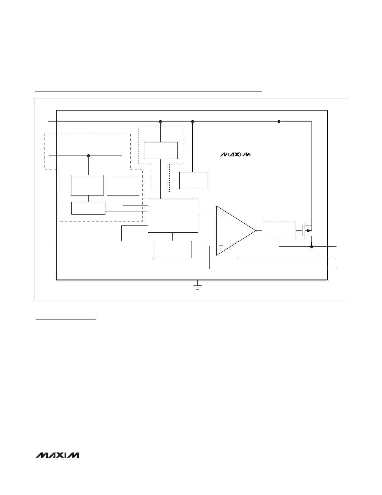
Functional Diagram
Detailed Description
The MAX15029/MAX15030 low-dropout linear regulators operate from input voltages as low as 1.425V and
deliver up to 500mA of continuous output current with a
maximum dropout voltage of only 150mV.
The MAX15030 operates with an input voltage as low
as 1.425V if the bias voltage (V
BIAS
) of 3V to 5.5V is
available. The power is applied at IN while the control
is provided through BIAS input. The current drawn by
BIAS is negligible when the LDO goes into the shutdown. This feature is especially useful in automotive
applications where the BIAS input is derived from an
always-on LDO that expects to provide minimal power
during the key-off condition.
The pMOS output stage can be driven from input voltages down to +1.425V without sacrificing stability or
transient performance. The output voltage of all the
regulators is adjustable from 0.5V to VINand is ±2%
accurate over load and line variations, from -40°C to
+125°C. Since these regulators have a pMOS output
device, supply current is not a significant function of
load or input headroom.
IN
BIAS
EN
MAX15030
ONLY
INTERNAL
SUPPLY
GENERATOR
REF
BIAS
UVLO
MAX15029
ONLY
REF
CONTROL
LOGIC
OVERTEMPERATURE
PROTECTION
IN
UVLO
MAX15029
MAX15030
ERROR
AMPLIFIER
WITH
SOFT-START
MOS DRIVER
WITH I
LIMIT
P
OUT
SS
FB
GND
Page 8

MAX15029/MAX15030
Internal p-Channel Pass Transistor
The MAX15029/MAX15030 feature a 75mΩ (typ)
p-channel MOSFET pass transistor. Unlike similar
designs using pnp pass transistors, p-channel
MOSFETs require no base drive, reducing quiescent
current. pnp-based regulators also waste considerable
current in dropout when the pass transistor saturates
and uses high base-drive currents under large loads.
The MAX15029/MAX15030 do not suffer from these
problems and consume only 315µA (typ) of quiescent
current under heavy loads, as well as in dropout.
Short-Circuit/
Thermal Fault Protection
The MAX15029/MAX15030 are fully protected from a
short circuit at the output through current-limiting and
thermal-overload circuitry. In the fault condition when
the output is shorted to ground, the output current is
limited to a maximum of 1A. Under these conditions,
the device quickly heats up. When the junction temperature reaches +165°C (typ), the thermal-overload circuitry turns off the output, allowing the part to cool
down. When the junction temperature cools to +150°C
(typ), the output turns back on and reestablishes regulation. Current limiting and thermal protection continue
until the fault is removed. For continuous operation, do
not exceed the absolute maximum junction-temperature rating of TJ= +150°C.
Soft-Start
The MAX15029/MAX15030 feature a soft-start function
that slowly ramps up the output voltage of the regulator
based on the value of the capacitor (CSS) connected
from SS to GND. Upon power-up, CSSis charged with
a 5µA (typ) current source through SS. The voltage at
SS is compared to the internal 0.5V reference (V
REF
).
The feedback voltage for regulation (V
REG
) is the lower
of VSSor V
REF
. As VSSrises, the regulation voltage
(V
REG
) rises at the same rate. Once VSSreaches and
rises above V
REF
, the regulation voltage then tracks the
reference voltage since it is the lower of VSSand V
REF
.
The value of CSSdetermines the length of the soft-start
time, tSS. Use the following formula to determine CSS.
C
SS
= 10-5x t
SS
where CSSis in farads and tSSis in seconds.
Shutdown Mode
The MAX15029/MAX15030 include an enable input. To
shut down the IC, drive EN low. In shutdown mode, the
current drawn by BIAS is less than 2µA. This feature is
extremely useful in an automotive application where the
BIAS input is derived from an always-on LDO expecting
to provide minimal dark current. For normal operation,
drive EN high or connect EN to IN for continuous on
operation. During shutdown, an internal 10kΩ resistor is
connected between OUT and GND.
Applications Information
Programming the Output Voltage
The MAX15029/MAX15030 feature an adjustable output
voltage from 0.5V to VINusing two external resistors
connected as a voltage-divider to FB as shown in
Figure 1. The output voltage is set by the following
equation:
where typically VFB= 0.5V. Choose R2 to be 10kΩ. Or,
to optimize load-transient response for no load to full
load transients, use the resistor-divider as a minimum
load and choose R2 to be 500Ω. To simplify resistor
selection:
1.425V to 3.6V Input, 500mA Low-Dropout
Regulators with BIAS Input
8 _______________________________________________________________________________________
Figure 1. MAX15030 Typical Application Circuit
R
1
⎛
VV
=+
OUT FB
⎛
V
RR
12 1=
ALWAYS-ON
INPUT
3V TO 5.5V
INPUT
1.425V TO 3.6V
1µF
BIAS
IN
OUT
⎜
V
⎝
MAX15030
ENABLE
EN
SHUTDOWN
SS
0.1uF
⎜
⎝
FB
⎞
1
⎟
⎠
R
2
⎞
−
⎟
⎠
OUT
FB
I.C.
GND
OUTPUT
R1
2.2µF
R2
Page 9

Capacitor Selection and
Regulator Stability
Capacitors are required at the MAX15029/MAX15030’s
inputs and outputs for stable operation over the full
temperature range and with load currents up to
500mA. Connect a 1µF capacitor between IN and
ground and a 2.2µF capacitor with low equivalent
series resistance (ESR) between OUT and ground for
500mA output current.
The input capacitor (C
IN
) lowers the source impedance
of the input supply. If input supply source impedance is
high, place a larger input capacitor close to IN to prevent VINsagging due to load transients. Smaller output
capacitors can be used for output currents less than
500mA. Calculate the minimum C
OUT
as follows:
Operating Region and
Power Dissipation
The maximum power dissipation depends on the thermal resistance of the IC package and circuit board, the
temperature difference between the die junction and
ambient air, and the rate of airflow. The power dissipated in the device is P
DISS
= I
OUT(VIN
- V
OUT
). The
package features an exposed thermal pad on its
underside. This pad lowers the thermal resistance of
the package by providing a direct heat conduction
path from the die to the PCB. Additionally, the ground
pins (GND) perform the dual function of providing an
electrical connection to system ground and channeling
heat away. Connect the exposed backside pad and
GND to the system ground using a large pad or ground
plane and multiple vias to the ground plane layer.
Noise, PSRR, and Transient Response
The MAX15029/MAX15030 are designed to operate
with low-dropout voltages and low quiescent currents
while still maintaining good noise performance, transient response, and AC rejection (see the
Typical
Operating Characteristics
). When operating from noisy
sources, improved supply-noise rejection and transient
response can be achieved by increasing the values of
the input and output bypass capacitors and through
passive filtering techniques. The MAX15029/MAX15030
load-transient response graphs (see the
Typical
Operating Characteristic
s) show two components of the
output response: a DC shift from the output impedance
due to the load current change, and the transient
response. A typical transient overshoot for a step
change in the load current from 100mA to 500mA is
10mV. Use ceramic output capacitors greater than
2.2µF (up to 100µF) to attenuate the overshoot.
Layout Guidelines
The TDFN package has an exposed thermal pad on its
underside. This pad provides a low thermal resistance
path for heat transfer into the PCB. This low thermally
resistive path carries a majority of the heat away from
the IC. The PCB is effectively a heatsink for the IC. The
exposed pad should be connected to a large ground
plane for proper thermal and electrical performance.
The minimum size of the ground plane is dependent
upon many system variables. To create an efficient
path, the exposed pad should be soldered to a thermal
landing, which is connected to the ground plane by
thermal vias. The thermal landing should be at least as
large as the exposed pad.
MAX15029/MAX15030
1.425V to 3.6V Input, 500mA Low-Dropout
Regulators with BIAS Input
_______________________________________________________________________________________ 9
CI
OUT OUT MAX
µ
F
=×
()
⎛
⎜
⎝
.1025
⎞
⎟
⎠
A
Page 10
MAX15029/MAX15030
1.425V to 3.6V Input, 500mA Low-Dropout
Regulators with BIAS Inputa
Maxim cannot assume responsibility for use of any circuitry other than circuitry entirely embodied in a Maxim product. No circuit patent licenses are
implied. Maxim reserves the right to change the circuitry and specifications without notice at any time.
10
____________________Maxim Integrated Products, 120 San Gabriel Drive, Sunnyvale, CA 94086 408-737-7600
© 2009 Maxim Integrated Products Maxim is a registered trademark of Maxim Integrated Products, Inc.
Chip Information
PROCESS: BiCMOS
INPUT
1.425V TO 3.6V
OUTPUT
0.5V TO V
IN
2.2µF
1µF
IN
OUT
FB
GND
EN
SS
MAX15029
INPUT
1.425V TO 3.6V
ALWAYS-ON INPUT
3V TO 5.5V
OUTPUT
0.5V TO V
IN
2.2µF
1µF
IN
BIAS
OUT
FB
GND
EN
SS
MAX15030
Typical Operating Circuits
1
3
4
10
8
7
OUT
GND
FB
IN
BIAS
I.C.
MAX15030
29
OUTIN
56
SSEN
TDFN
(3mm x 3mm)
TOP VIEW
Pin Configurations (continued)
Package Information
For the latest package outline information and land patterns, go
to www.maxim-ic.com/packages
.
PACKAGE TYPE PACKAGE CODE DOCUMENT NO.
10 TDFN-EP* T1033-1
21-0137
*
EP = Exposed pad.
+
 Loading...