

Page 1
General Description
The MAX15026 synchronous step-down controller operates from a 4.5V to 28V input voltage range and generates an adjustable output voltage from 85% of the input
voltage down to 0.6V while supporting loads up to 25A.
The device allows monotonic startup into a prebiased
bus without discharging the output and features adaptive internal digital soft-start.
The MAX15026 offers the ability to adjust the switching
frequency from 200kHz to 2MHz with an external resistor. The MAX15026’s adaptive synchronous rectification
eliminates the need for an external freewheeling
Schottky diode. The device also utilizes the external
low-side MOSFET’s on-resistance as a current-sense
element, eliminating the need for a current-sense resistor. This protects the DC-DC components from damage
during output overloaded conditions or output shortcircuit faults without requiring a current-sense resistor.
Hiccup-mode current limit reduces power dissipation
during short-circuit conditions. The MAX15026 includes
a power-good output and an enable input with precise
turn-on/turn-off threshold, which can be used for input
supply monitoring and for power sequencing.
Additional protection features include sink-mode current limit and thermal shutdown.
Sink-mode current limit prevents reverse inductor current from reaching dangerous levels when the device is
sinking current from the output.
The MAX15026 is available in a space-saving and thermally enhanced 3mm x 3mm, 14-pin TDFN-EP package. The MAX15026 operates over the -40°C to +85°C
temperature range.
Applications
Set-Top Boxes
LCD TV Secondary Supplies
Switches/Routers
Power Modules
DSP Power Supplies
Points-of-Load Regulators
Features
o 4.5V to 28V or 5V ±10% Input Supply Range
o 0.6V to (0.85 x V
IN
) Adjustable Output
o Adjustable 200kHz to 2MHz Switching Frequency
o Ability to Start into a Prebiased Load
o Lossless, Cycle-by-Cycle Valley Mode Current
Limit with Adjustable, Temperature-Compensated
Threshold
o Sink-Mode Current-Limit Protection
o Adaptive Internal Digital Soft-Start
o ±1% Accurate Voltage Reference
o Internal Boost Diode
o Adaptive Synchronous Rectification Eliminates
External Freewheeling Schottky Diode
o Hiccup-Mode Short-Circuit Protection
o Thermal Shutdown
o Power-Good Output and Enable Input for Power
Sequencing
o ±5% Accurate Enable Input Threshold
MAX15026
Low-Cost, Small, 4.5V to 28V Wide Operating
Range, DC-DC Synchronous Buck Controller
________________________________________________________________
Maxim Integrated Products
1
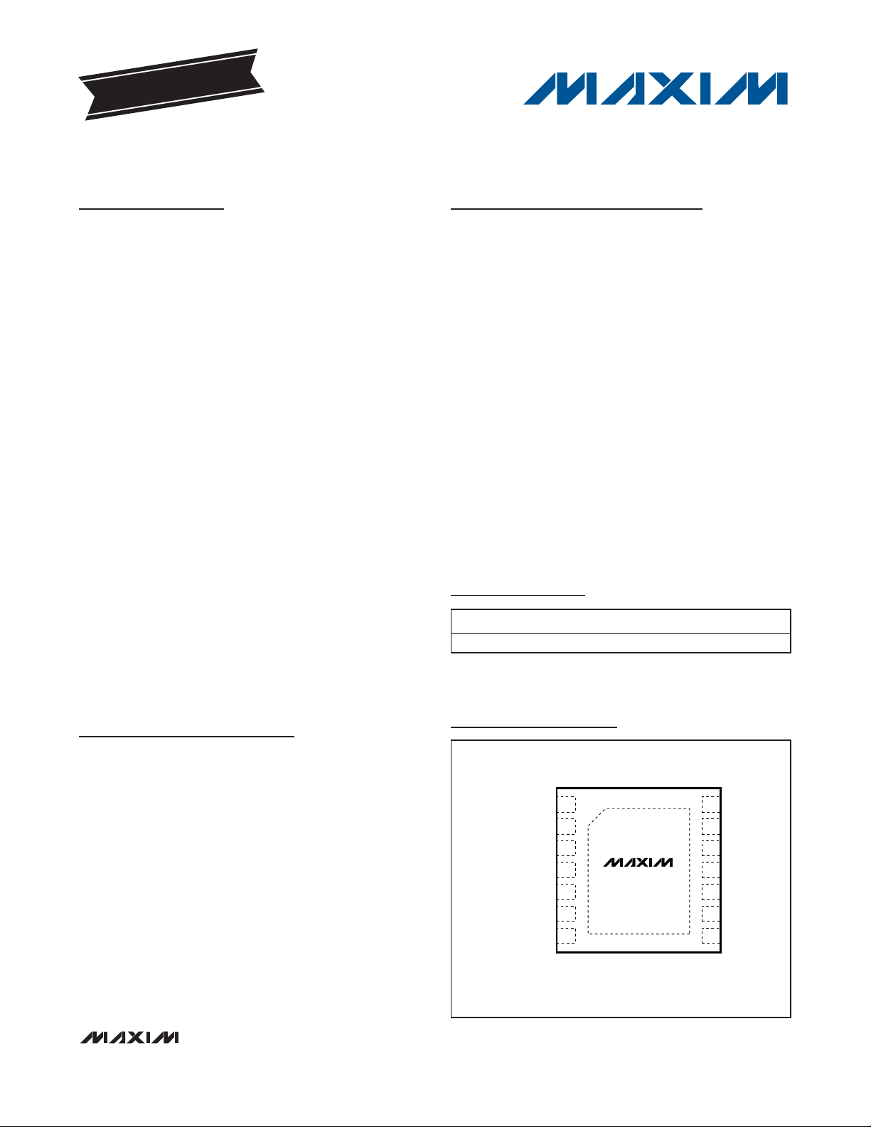
Pin Configuration
Ordering Information
19-4108; Rev 0; 5/08
For pricing, delivery, and ordering information, please contact Maxim Direct at 1-888-629-4642,
or visit Maxim’s website at www.maxim-ic.com.
EVALUATION KIT
AVAILABLE
PART TEMP RANGE
PIN-PACKAGE
-40°C to +85°C 14 TDFN-EP*
+
Denotes a lead-free package.
*
EP = Exposed pad.
MAX15026BETD+
TOP VIEW
1
+
V
2
CC
312
EN
4
LIM
5
69
78
MAX15026
*EP
DHIN
14
LX
13
BSTPGOOD
DL
11
DRV
10
GNDCOMP
RTFB
*EP = EXPOSED PAD.
TDFN
(3mm x 3mm)
Page 2
MAX15026
Low-Cost, Small, 4.5V to 28V Wide Operating
Range, DC-DC Synchronous Buck Controller
2 _______________________________________________________________________________________
ABSOLUTE MAXIMUM RATINGS
ELECTRICAL CHARACTERISTICS
(VIN= 12V, R
RT
= 27kΩ, R
LIM
= 30kΩ, C
VCC
= 4.7µF, CIN= 1µF, TA= -40°C to +85°C, unless otherwise noted. Typical values are at
T
A
= +25°C.) (Note 2)
Stresses beyond those listed under “Absolute Maximum Ratings” may cause permanent damage to the device. These are stress ratings only, and functional
operation of the device at these or any other conditions beyond those indicated in the operational sections of the specifications is not implied. Exposure to
absolute maximum rating conditions for extended periods may affect device reliability.
Note 1: Dissipation wattage values are based on still air with no heatsink. Actual maximum power dissipation is a function of heat
extraction technique and may be substantially higher. Package thermal resistances were obtained using the method
described in JEDEC specification JESD51-7, using a four-layer board. For detailed information on package thermal considerations, refer to www.maxim-ic.com/thermal-tutorial
.
IN to GND ...............................................................-0.3V to +30V
BST to GND ............................................................-0.3V to +36V
LX to GND .................................................................-1V to +30V
EN to GND................................................................-0.3V to +6V
PGOOD to GND .....................................................-0.3V to +30V
BST to LX..................................................................-0.3V to +6V
DH to LX ...............................................….-0.3V to (V
BST
+ 0.3V)
DRV to GND .............................................................-0.3V to +6V
DL to GND ................................................-0.3V to (V
DRV
+ 0.3V)
V
CC
to GND...............-0.3V to the lower of +6V and (VIN+ 0.3V)
All Other Pins to GND.................................-0.3V to (V
CC
+ 0.3V)
V
CC
Short Circuit to GND...........................................Continuous
DRV Input Current.............................................................600mA
PGOOD Sink Current ............................................................5mA
Continuous Power Dissipation (T
A
= +70°C) (Note 1)
14-Pin TDFN-EP, Multilayer Board
(derate 24.4mW/°C above +70°C)..............................1951mW
Operating Temperature Range ...........................-40°C to +85°C
Junction Temperature......................................................+150°C
Storage Temperature Range .............................-60°C to +150°C
Lead Temperature (soldering, 10s) .................................+300°C
GENERAL
Input Voltage Range V
Quiescent Supply Current V
Shutdown Supply Current I
Enable to Output Delay 480 µs
VCC High to Output Delay EN = V
VCC REGULATOR
Output Voltage V
VCC Regulator Dropout VIN = 4.5V, I
VCC Short-Circuit Output Current VIN = 5V 100 200 300 mA
VCC Undervoltage Lockout V
VCC Undervoltage Lockout
Hysteresis
ERROR AMPLIFIER (FB, COMP)
FB Input Voltage Set-Point V
FB Input Bias Current I
FB to COMP Transconductance g
Amplifier Open-Loop Gain 80 dB
Amplifier Unity-Gain Bandwidth Capacitor from COMP to GND = 50pF 4 MHz
V
COMP-RAMP
COMP Source/Sink Current I
PARAMETER SYMBOL CONDITIONS MIN TYP MAX UNITS
Minimum Voltage 160 mV
IN
IN_SBY
CC
CC_UVLOVCC
FB
FB
M
COMP
VIN = VCC = V
= 0.9V, no switching 1.75 2.75 mA
FB
EN = GND 290 500 µA
6V < VIN < 28V, I
VIN = 12V, 1mA < I
rising 3.8 4.0 4.2 V
V
= 0.6V -250 +250 nA
FB
I
COMP
V
COMP
DRV
CC
LOAD
= ±20µA 600 1200 1800 µS
= 1.4V 50 80 110 µA
= 25mA
LOAD
< 70mA
LOAD
= 70mA 0.28 V
4.5 28
4.5 5.5
375 µs
5.0 5.25 5.5 V
400 mV
582 592 597 mV
V
Page 3
MAX15026
Low-Cost, Small, 4.5V to 28V Wide Operating
Range, DC-DC Synchronous Buck Controller
_______________________________________________________________________________________ 3
ELECTRICAL CHARACTERISTICS (continued)
(VIN= 12V, R
RT
= 27kΩ, R
LIM
= 30kΩ, C
VCC
= 4.7µF, CIN= 1µF, TA= -40°C to +85°C, unless otherwise noted. Typical values are at
T
A
= +25°C.) (Note 2)
ENABLE (EN)
EN Input High V
EN Input Low V
EN Input Leakage Current I
OSCILLATOR
Switching Frequency f
1MHz Switching Frequency RRT = 15.7kΩ 0.9 1 1.1 MHz
2MHz Switching Frequency RRT = 7.2kΩ 1.8 2.0 2.4 MHz
Switching Frequency Adjustment
Range (Note 3)
RT Voltage V
PWM Ramp Peak-to-Peak
DRV Undervoltage Lockout
Hysteresis
DH On-Resistance
DL On-Resistance
DH Peak Current C
DL Peak Current C
DH/DL Break-Before-Make Time
SOFT-START
Soft-Start Duration 2048
Reference Voltage Steps 64 Steps
CURRENT LIMIT/HICCUP
Current-Limit Threshold
Adjustment Range
PARAMETER SYMBOL CONDITIONS MIN TYP MAX UNITS
EN_H
EN_L
LEAK_ENVEN
SW
RT
V
DRV_UVLOVDRV
V
VEN falling 0.997 1.05 1.103 V
RRT = 27kΩ 540 600 660 kHz
Low, sinking 100mA, V
High, sourcing 100mA, V
Low, sinking 100mA, V
High, sourcing 100mA, V
Time from high side at 1V to low side at
1V
Cycle-by-cycle valley currentlimit threshold adjustment range
valley limit = V
rising 1.14 1.20 1.26 V
EN
= 5.5V -1 +1 µA
200 2000 kHz
1.19 1.205 1.22 V
rising 4.0 4.2 4.4 V
400 mV
= 5V 1 3
BST
= 5V 1.5 4.5
BST
= 5.2V 1 3
DRV
= 5.2V 1.5 4.5
DRV
LOAD
LOAD
= 10nF
= 10nF
LIM
Sinking 1.8
Sourcing 2
Sinking 3
Sourcing 2.4
10 ns
30 300 mV
/10
Switching
Cycles
Ω
Ω
A
A
Page 4
MAX15026
Low-Cost, Small, 4.5V to 28V Wide Operating
Range, DC-DC Synchronous Buck Controller
4 _______________________________________________________________________________________
ELECTRICAL CHARACTERISTICS (continued)
(VIN= 12V, R
RT
= 27kΩ, R
LIM
= 30kΩ, C
VCC
= 4.7µF, CIN= 1µF, TA= -40°C to +85°C, unless otherwise noted. Typical values are at
T
A
= +25°C.) (Note 2)
Note 2: All devices are 100% tested at room temperature and guaranteed by design over the specified temperature range.
Note 3: Select R
RT
as: where fSWis in Hertz.
Note 4: T
A
= +25°C.
LIM Reference Current I
LIM Reference Current Tempco V
Number of Consecutive CurrentLimit Events to Hiccup
Soft-Start Timeout 4096
Soft-Start Restart Timeout 8192
Hiccup Timeout Out of soft-start 4096
Peak Low-Side Sink Current
Limit
BOOST
Boost Switch Resistance VIN = VCC = 5V, I
POWER-GOOD OUTPUT
PARAMETER SYMBOL CONDITIONS MIN TYP MAX UNITS
V
LIM
= 0.3V to 3V (Note 4) 45 50 55 µA
LIM
= 0.3V to 3V 2300 ppm/°C
LIM
7 Events
Sink limit = 1.5V, R
= 30kΩ (Note 4) 75 mV
LIM
= 10mA 3 8 Ω
BST
Switching
Cycles
Switching
Cycles
Switching
Cycles
PGOOD Threshold Rising 88 93 97 % V
PGOOD Threshold Falling 86 90 94 %V
PGOOD Output Leakage I
PGOOD Output Low Voltage V
THERMAL SHUTDOWN
Thermal-Shutdown Threshold Temperature rising +150 °C
Thermal-Shutdown Hysteresis Temperature falling 20 °C
R
=
RT
LEAK_PGD
PGOOD_LIPGOOD
17.3 10
()
f 1x10 )x(f
+
SW
VIN = V
9
×
SW
2
7
−
= 28V, VEN = 5V, VFB = 1V -1 +1 µA
PGOOD
= 2mA, EN = GND 0.4 V
FB
FB
Page 5
MAX15026
Low-Cost, Small, 4.5V to 28V Wide Operating
Range, DC-DC Synchronous Buck Controller
_______________________________________________________________________________________ 5
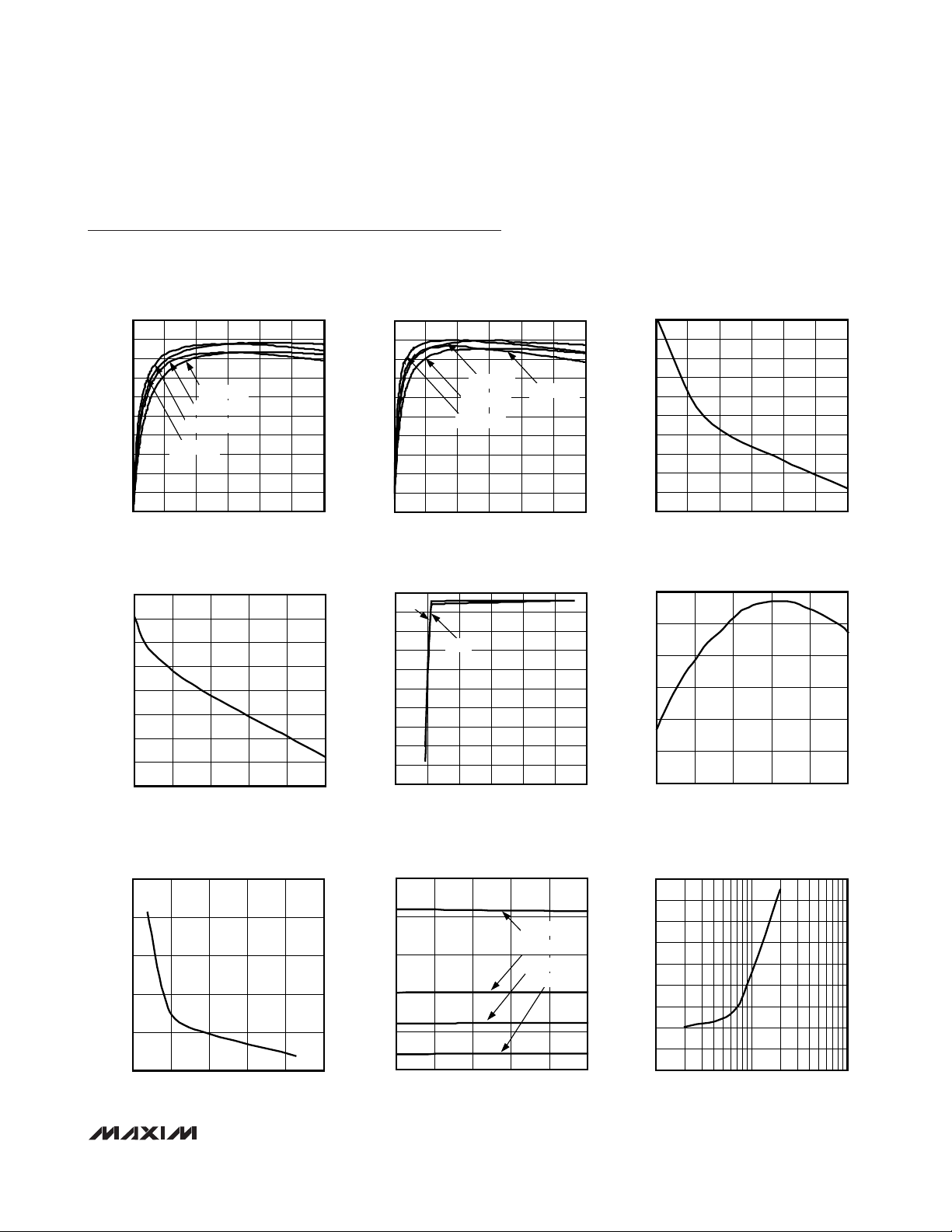
Typical Operating Characteristics
(VIN= 12V, TA= +25°C, unless otherwise noted.) (See the circuit of Figure 5.)
EFFICIENCY vs. LOAD CURRENT
100
90
80
70
60
50
40
EFFICIENCY (%)
30
20
10
0
012
V
OUT
V
= 1.2V
OUT
V
= 5V
OUT
V
= 1.8V
OUT
4
LOAD CURRENT (A)
= 3.3V
62
810
MAX15026 toc01
EFFICIENCY (%)
VCC vs. LOAD CURRENT
5.265
5.260
5.255
5.250
(V)
5.245
CC
V
5.240
5.235
5.230
5.225
0 100
LOAD CURRENT (mA)
60
40
8020
MAX15026 toc04
(V)
V
CC
EFFICIENCY vs. LOAD CURRENT
= 12V, VCC = V
(V
100
IN
90
80
70
60
50
40
30
20
10
0
V
V
OUT
4
2012
LOAD CURRENT (A)
V
OUT
= 5V
OUT
= 3.3V
= 1.8V
6
DRV
8
VCC LINE REGULATION
5.3
5mA
5.2
5.1
5.0
4.9
4.8
4.7
4.6
4.5
4.4
4.3
030
50mA
VIN (V)
= 5V)
V
OUT
10
= 1.2V
252015105
0
-0.1
-0.2
MAX15026 toc02
-0.3
-0.4
-0.5
-0.6
-0.7
% OUTPUT FROM NOMINAL
-0.8
-0.9
-1.0
5.248
5.246
MAX15026 toc05
5.244
(V)
5.242
CC
V
5.240
5.238
5.236
-40 85
V
vs. LOAD CURRENT
OUT
LOAD CURRENT (A)
VCC vs. TEMPERATURE
TEMPERATURE (°C)
MAX15026 toc03
106842012
MAX15026 toc06
603510-15
SWITCHING FREQUENCY
vs. RESISTANCE
2500
2000
1500
1000
SWITCHING FREQUENCY (kHz)
500
0
0 100
RESISTANCE (kΩ)
SWITCHING FREQUENCY
vs. TEMPERATURE
2500
2000
MAX15026 toc07
1500
1000
SWITCHING FREQUENCY (kHz)
500
0
80604020
-40 85
TEMPERATURE (°C)
RRT = 7.2k
RRT = 15.7k
RRT = 27k
RRT = 85k
603510-15
Ω
Ω
Ω
Ω
90
80
MAX15026 toc08
70
60
50
40
30
SUPPLY CURRENT (mA)
20
10
0
100 10,000
SUPPLY CURRENT
vs. SWITCHING FREQUENCY
MAX15026 toc09
1000
SWITCHING FREQUENCY (kHz)
Page 6
MAX15026
Low-Cost, Small, 4.5V to 28V Wide Operating
Range, DC-DC Synchronous Buck Controller
6 _______________________________________________________________________________________
Typical Operating Characteristics (continued)
(VIN= 12V, TA= +25°C, unless otherwise noted.) (See the circuit of Figure 5.)
LIM REFERENCE CURRENT
vs. TEMPERATURE
MAX15026 toc10
TEMPERATURE (°C)
LIM REFERENCE CURRENT (µA)
603510-15
10
20
30
40
50
60
70
0
-40 85
SINK AND SOURCE CURRENT-LIMIT
THRESHOLDS vs. RESISTANCE (R
ILIM
)
MAX15026 toc11
RESISTANCE (kΩ)
CURRENT-LIMIT THRESHOLDS (V)
605040302010
-0.3
-0.2
-0.1
0
0.1
0.2
-0.4
070
SINK CURRENT-LIMIT
SOURCE CURRENT-LIMIT
LOAD TRANSIENT ON OUT
MAX15026 toc12
400µs/div
AC-COUPLED
V
OUT
200mV/div
I
OUT
10A
1A
STARTUP AND DISABLE FROM EN
(R
LOAD
= 1.5Ω)
MAX15026 toc13
4ms/div
V
OUT
1V/div
V
IN
5V/div
PGOOD
5V/div
STARTUP RISE TIME
MAX15026 toc14
1ms/div
V
IN
5V/div
V
OUT
1V/div
POWER-DOWN FALL TIME
MAX15026 toc15
4ms/div
V
IN
5V/div
V
OUT
1V/div
STARTUP WITH PREBIASED
OUTPUT (1.5V)
MAX15026 toc16
1ms/div
V
IN
5V/div
V
OUT
1V/div
0.5V OUTPUT PREBIAS
STARTUP WITH PREBIASED
OUTPUT (1.5V)
MAX15026 toc17
2ms/div
V
IN
5V/div
V
OUT
1V/div
2V OUTPUT PREBIAS
OUTPUT SHORT-CIRCUIT BEHAVIOR MONITOR
OUTPUT VOLTAGE AND CURRENT
MAX15026 toc18
4ms/div
500mV/div
0
V
OUT
I
OUT
20A/div
0
Page 7
MAX15026
Low-Cost, Small, 4.5V to 28V Wide Operating
Range, DC-DC Synchronous Buck Controller
_______________________________________________________________________________________ 7
Pin Description
PIN NAME FUNCTION
1IN
2V
3 PGOOD Open-Drain Power-Good Output. Connect PGOOD with an external resistor to any supply voltage.
4EN
5 LIM
6 COMP
7FB
8RT
9 GND Ground
10 DRV
11 DL Low-Side Gate-Driver Output. DL swings from DRV to GND. DL is low during UVLO.
12 BST
CC
Regulator Input. Bypass IN to GND with a 1µF minimum ceramic capacitor. Connect IN to V
operating in the 5V ±10% range.
5.25V Linear Regulator Output. Bypass VCC to GND with a minimum of 4.7µF low-ESR ceramic
capacitor to ensure stability up to the regulated rated current when V
DRV. Bypass V
minimum ceramic capacitor.
Active-High Enable Input. Pull EN to GND to disable the output. Connect EN to V
operation. EN can be used for power sequencing and as a UVLO adjustment input.
Current-Limit Adjustment. Connect a resistor from LIM to GND to adjust current-limit threshold from
30mV (R
Compensation Input. Connect compensation network from COMP to FB or from COMP to GND. See
the Compensation section.
Feedback Input. Connect FB to a resistive divider between output and GND to adjust the output
voltage between 0.6V and (0.85 x Input Voltage). See the Setting the Output Voltage section.
Oscillator Timing Resistor Input. Connect a resistor from RT to GND to set the oscillator frequency
from 200kHz to 2MHz. See the Setting the Switching Frequency section.
Drive Supply Voltage. DRV is internally connected to the anode terminal of the internal boost diode.
Bypass DRV to GND with a 2.2µF minimum ceramic capacitor (see the Typical Application Circuits).
Boost Flying Capacitor. Connect a ceramic capacitor with a minimum value of 100nF between BST
and LX.
LIM
to GND when VCC supplies the device core quiescent current with a 2.2µF
CC
= 6kΩ) to 300mV (R
= 60kΩ). See the Setting the Valley Current Limit section.
LIM
supplies the drive current at
CC
for always-on
CC
CC
when
External Inductor Connection. Connect LX to the switching side of the inductor. LX serves as the
13 LX
14 DH High-Side Gate-Driver Output. DH swings from LX to BST. DH is low during UVLO.
—EP
lower supply rail for the high-side gate driver and as a sensing input of the drain to source voltage
drop of the synchronous MOSFET.
Exposed Paddle. Internally connected to GND. Connect EP to a large copper plane at GND potential
to improve thermal dissipation. Do not use EP as the only GND ground connection.
Page 8

MAX15026
Low-Cost, Small, 4.5V to 28V Wide Operating
Range, DC-DC Synchronous Buck Controller
8 _______________________________________________________________________________________
Functional Diagram
MAX15026
V
RT
EN
V
REF
V
BGAP
GENERATOR
ENABLE
COMPARATOR
BANDGAP
OK
REF
EN_INT
BGAP_OK
BGAP_OK
OSCILLATOR
CK
OSC_ENABLE
V
REF
HICCUP
CK
ENABLE
V
REF
CK
SOFT-START/
SOFT-STOP
LOGIC AND
HICCUP LOGIC
RAMP
GENERATOR
FB1
DAC_VREF
HICCUP TIMEOUT
DH_DL_ENABLE
RAMP
g
M
PWM
COMPARATOR
PWM
COMP
V
LIM
CC
IN
VIN_OK
V
BGAP
BGAP_OK
BGAP_OK
V
DRV
VIN_OK
INTERNAL
VOLTAGE
REGULATOR
V
CC
UVLO
DRV
UVLO
THERMAL
SHUTDOWN
AND ILIM
CURRENT
GEN
IN
UVLO
VL_OK
VDRV_OK
SHUTDOWN
VIN_OK
V
V
BGAP
REF
DC-DC
AND
OSCILLATOR
ENABLE
LOGIC
VIN_OK
I
BIAS
= 0.6V
= 1.24V
DH_DL_ENABLE
MAIN
BIAS
CURRENT
GENERATOR
BANDGAP
REFERENCE
HICCUP
TIMEOUT
CK
SINK
CURRENT-LIMIT
COMPARATOR
VALLEY
CURRENT-LIMIT
COMPARATOR
PWM
CONTROL
LOGIC
HICCUP
LIM/20
LIM/10
BOOST
DRIVER
V
REF
GATEP
HIGH-
SIDE
DRIVER
LOW-
SIDE
DRIVER
ENABLE
PGOOD
COMPARATOR
BST
DH
LX
DRV
DL
GND
FB
PGOOD
GND
Page 9

MAX15026
Low-Cost, Small, 4.5V to 28V Wide Operating
Range, DC-DC Synchronous Buck Controller
_______________________________________________________________________________________ 9
Detailed Description
The MAX15026 synchronous step-down controller operates from a 4.5V to 28V input voltage range and generates an adjustable output voltage from 85% of the input
voltage down to 0.6V while supporting loads up to 25A.
As long as the device supply voltage is within 5.0V to
5.5V, the input power bus (VIN) can be as low as 3.3V.
The MAX15026 offers adjustable switching frequency
from 200kHz to 2MHz with an external resistor. The
adjustable switching frequency provides design flexibility in selecting passive components. The MAX15026
adopts an adaptive synchronous rectification to eliminate an external freewheeling Schottky diode and
improve efficiency. The device utilizes the on-resistance of the external low-side MOSFET as a currentsense element. The current-limit threshold voltage is
resistor-adjustable from 30mV to 300mV and is temperature-compensated, so that the effects of the MOSFET
R
DS(ON)
variation over temperature are reduced. This
current-sensing scheme protects the external components from damage during output overloaded conditions or output short-circuit faults without requiring a
current-sense resistor. Hiccup-mode current limit
reduces power dissipation during short-circuit conditions. The MAX15026 includes a power-good output
and an enable input with precise turn-on/-off threshold
to be used for monitoring and for power sequencing.
The MAX15026 features internal digital soft-start that
allows prebias startup without discharging the output.
The digital soft-start function employs sink current limiting to prevent the regulator from sinking excessive current when the prebias voltage exceeds the
programmed steady-state regulation level. The digital
soft-start feature prevents the synchronous rectifier
MOSFET and the body diode of the high-side MOSFET
from experiencing dangerous levels of current while the
regulator is sinking current from the output. The
MAX15026 shuts down at a junction temperature of
+150°C to prevent damage to the device.
DC-DC PWM Controller
The MAX15026 step-down controller uses a PWM voltage-mode control scheme (see the
Functional Diagram
).
Control-loop compensation is external for providing maximum flexibility in choosing the operating frequency and
output LC filter components. An internal transconductance error amplifier produces an integrated error voltage at COMP that helps to provide higher DC accuracy.
The voltage at COMP sets the duty cycle using a PWM
comparator and a ramp generator. On the rising edge of
an internal clock, the high-side n-channel MOSFET turns
on and remains on until either the appropriate duty cycle
or the maximum duty cycle is reached. During the ontime of the high-side MOSFET, the inductor current
ramps up. During the second-half of the switching cycle,
the high-side MOSFET turns off and the low-side n-channel MOSFET turns on. The inductor releases the stored
energy as the inductor current ramps down, providing
current to the output. Under overload conditions, when
the inductor current exceeds the selected valley currentlimit threshold (see the
Current-Limit Circuit (LIM)
section), the high-side MOSFET does not turn on at the
subsequent clock rising edge and the low-side MOSFET
remains on to let the inductor current ramp down.
Internal 5.25V Linear Regulator
An internal linear regulator (VCC) provides a 5.25V nominal supply to power the internal functions and to drive
the low-side MOSFET. Connect IN and V
CC
together
when using an external 5V ±10% power supply. The
maximum regulator input voltage (VIN) is 28V. Bypass IN
to GND with a 1µF ceramic capacitor. Bypass the output
of the linear regulator (VCC) with a 4.7µF ceramic capacitor to GND. The VCCdropout voltage is typically 125mV.
When VINis higher than 5.5V, VCCis typically 5.25V. The
MAX15026 also employs an undervoltage lockout circuit
that disables the internal linear regulator when VCCfalls
below 3.6V (typ). The 400mV UVLO hysteresis prevents
chattering on power-up/power-down.
The internal VCClinear regulator can source up to
70mA to supply the IC, power the low-side gate driver,
recharge the external boost capacitor, and supply small
external loads. The current available for external loads
depends on the current consumed by the MOSFET
gate drivers.
For example, when switching at 600kHz, a MOSFET
with 18nC total gate charge (at V
GS
= 5V) requires
(18nC x 600kHz) = 11mA. The internal control functions
consume 5mA maximum. The current available for
external loads is:
(70 – (2 x 11) – 5)mA ≅ 43mA
MOSFET Gate Drivers (DH, DL)
DH and DL are optimized for driving large-size n-channel power MOSFETs. Under normal operating conditions and after startup, the DL low-side drive waveform
is always the complement of the DH high-side drive
waveform, with controlled dead-time to prevent crossconduction or shoot-through. An adaptive dead-time
circuit monitors the DH and DL outputs and prevents
the opposite-side MOSFET from turning on until the
other MOSFET is fully off. Thus, the circuit allows the
high-side driver to turn on only when the DL gate driver
has turned off, preventing the low-side (DL) from turning on until the DH gate driver has turned off.
Page 10

MAX15026
The adaptive driver dead-time allows operation without
shoot-through with a wide range of MOSFETs, minimizing delays and maintaining efficiency. There must be a
low-resistance, low-inductance path from DL and DH to
the MOSFET gates for the adaptive dead-time circuits
to function properly. The stray impedance in the gate
discharge path can cause the sense circuitry to interpret the MOSFET gate as off while the VGSof the
MOSFET is still high. To minimize stray impedance, use
very short, wide traces.
Synchronous rectification reduces conduction losses in
the rectifier by replacing the normal low-side Schottky
catch diode with a low-resistance MOSFET switch. The
MAX15026 features a robust internal pulldown transistor with a typical 1Ω R
DS(ON)
to drive DL low. This low
on-resistance prevents DL from being pulled up during
the fast rise time of the LX node, due to capacitive coupling from the drain to the gate of the low-side synchronous rectifier MOSFET.
High-Side Gate-Drive Supply (BST)
and Internal Boost Switch
An internal switch between BST and DH turns on to
boost the gate voltage above VINproviding the necessary gate-to-source voltage to turn on the high-side
MOSFET. The boost capacitor connected between BST
and LX holds up the voltage across the floating gate
driver during the high-side MOSFET on-time.
The charge lost by the boost capacitor for delivering the
gate charge is replenished when the high-side MOSFET
turns off and LX node goes to ground. When LX is low,
an internal high-voltage switch connected between
V
DRV
and BST recharges the boost capacitor. See the
Boost Capacitor
section in the
Applications Information
to choose the right size of the boost capacitor.
Enable Input (EN), Soft-Start,
and Soft-Stop
Drive EN high to turn on the MAX15026. A soft-start
sequence starts to increase step-wise the reference
voltage of the error amplifier. The duration of the softstart ramp is 2048 switching cycles and the resolution
is 1/64th of the steady-state regulation voltage allowing
a smooth increase of the output voltage. A logic-low on
EN initiates a soft-stop sequence by stepping down the
reference voltage of the error amplifier. After the soft-
stop sequence is completed, the MOSFET drivers are
both turned off. See Figure 1.
Connect EN to VCCfor always-on operation. Owing to
the accurate turn-on/-off thresholds, EN can be used as
UVLO adjustment input, and for power sequencing
together with the PGOOD output.
When the valley current limit is reached during soft-start
the MAX15026 regulates to the output impedance times
the limited inductor current and turns off after 4096
clock cycles. When starting up into a large capacitive
load (for example) the inrush current will not exceed the
current-limit value. If the soft-start is not completed
before 4096 clock cycles, the device will turn off. The
device remains off for 8192 clock cycles before trying
to soft-start again. This implementation allows the softstart time to be automatically adapted to the time necessary to keep the inductor current below the limit while
charging the output capacitor.
Power-Good Output (PGOOD)
The MAX15026 includes a power-good comparator to
monitor the output voltage and detect the power-good
threshold, fixed at 93% of the nominal FB voltage. The
open-drain PGOOD output requires an external pullup
resistor. PGOOD sinks up to 2mA of current while low.
PGOOD goes high (high-impedance) when the regulator output increases above 93% of the designed nominal regulated voltage. PGOOD goes low when the
regulator output voltage drops to below 90% of the
nominal regulated voltage. PGOOD asserts low during
hiccup timeout period.
Startup into a Prebiased Output
When the MAX15026 starts into a prebiased output, DH
and DL are off so that the converter does not sink current from the output. DH and DL do not start switching
until the PWM comparator commands the first PWM
pulse. The first PWM pulse occurs when the ramping
reference voltage increases above the FB voltage.
When the output voltage is biased above the output
set-point, the controller tries to pull the output down to
the set-point once the internal soft-start is complete.
This pulldown is limited by the sink current limit, which
is slowly increased to its normal value to minimize output undershoot.
Low-Cost, Small, 4.5V to 28V Wide Operating
Range, DC-DC Synchronous Buck Controller
10 ______________________________________________________________________________________
Page 11
Current-Limit Circuit (LIM)
The current-limit circuit employs a valley and sink current-sensing algorithm that uses the on-resistance of
the low-side MOSFET as a current-sensing element, to
eliminate costly sense resistors. The current-limit circuit
is also temperature compensated to track the on-resistance variation of the MOSFET over temperature. The
current limit is adjustable with an external resistor at
LIM, and accommodates MOSFETs with a wide range
of on-resistance characteristics (see the
Setting the
Valley Current Limit
section). The adjustment range is
from 30mV to 300mV for the valley current limit, corresponding to resistor values of 6kΩ to 60kΩ. The valley
current-limit threshold across the low-side MOSFET is
precisely 1/10th of the voltage at LIM, while the sink
current-limit threshold is 1/20th of the voltage at LIM.
Valley current limit acts when the inductor current flows
towards the load, and LX is more negative than GND
during the low-side MOSFET on-time. If the magnitude
of current-sense signal exceeds the valley current-limit
threshold at the end of the low-side MOSFET on-time,
the MAX15026 does not initiate a new PWM cycle and
lets the inductor current decay in the next cycle. The
controller also rolls back the internal reference voltage
so that the controller finds a regulation point determined by the current-limit value and the resistance of
the short. In this manner, the controller acts as a constant current source. This method greatly reduces
inductor ripple current during the short event, which
reduces inductor sizing restrictions, and reduces the
possibility for audible noise. After a timeout, the device
goes into hiccup mode. Once the short is removed, the
internal reference voltage soft-starts back up to the normal reference voltage and regulation continues.
MAX15026
Low-Cost, Small, 4.5V to 28V Wide Operating
Range, DC-DC Synchronous Buck Controller
______________________________________________________________________________________ 11
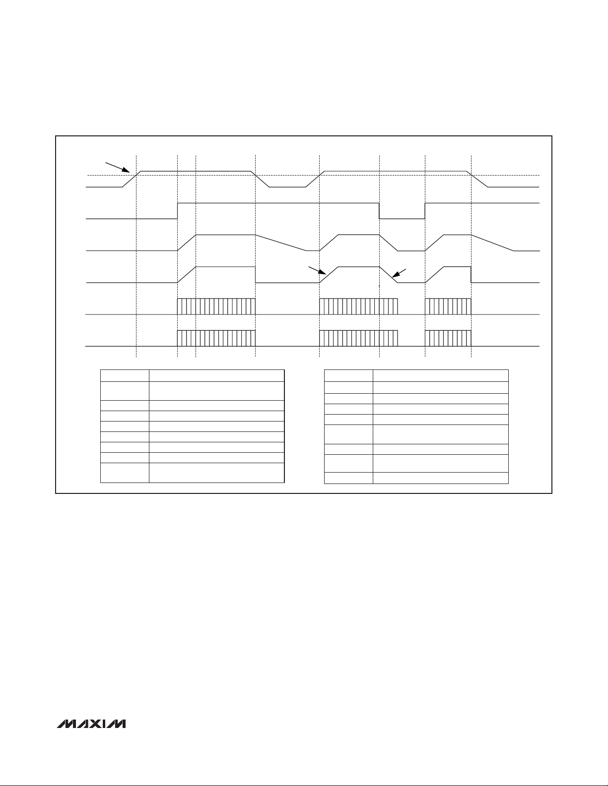
Figure 1. Power-On/-Off Sequencing
UVLO
V
EN
V
OUT
DAC_VREF
DH
CD
B
CC
DL
SYMBOL DEFINITION
UVLO
V
CC
EN
V
OUT
DAC_VREF
DH
DL
A
Undervoltage threshold value is provided in
the Electrical Characteristics table.
Internal 5.25V linear regulator output.
Active-high enable input.
Regulator output voltage.
Regulator internal soft-start and soft-stop signal.
Regulator high-side gate-driver output.
Regulator low-side gate-driver output.
V
rising while below the UVLO threshold.
CC
EN is low.
E
2048 CLK
CYCLES
F
SYMBOL DEFINITION
B
C
D
E
F
G
H
I
G
2048 CLK
CYCLES
V
is higher than the UVLO threshold. EN is low.
CC
EN is pulled high. DH and DL start switching.
Normal operation.
drops below UVLO.
V
CC
V
goes above the UVLO threshold. DH and DL
CC
start switching. Normal operation.
EN is pulled low. V
EN is pulled high. DH and DL start switching.
Normal operation.
V
drops below UVLO.
CC
HIA
enters soft-stop.
OUT
Page 12

MAX15026
Sink current limit is implemented by monitoring the voltage drop across the low-side MOSFET when LX is more
positive than GND. When the voltage drop across the
low-side MOSFET exceeds 1/20th of the voltage at LIM
at any time during the low-side MOSFET on-time, the
low-side MOSFET turns off, and the inductor current
flows from the output through the body diode of the highside MOSFET. When the sink current limit activates, the
DH/DL switching sequence is no longer complementary.
Carefully observe the PCB layout guidelines to ensure
that noise and DC errors do not corrupt the currentsense signals at LX and GND. Mount the MAX15026
close to the low-side MOSFET with short, direct traces
making a Kelvin-sense connection so that trace resistance does not add to the intended sense resistance of
the low-side MOSFET.
Hiccup-Mode Overcurrent Protection
Hiccup-mode overcurrent protection reduces power dissipation during prolonged short-circuit or deep overload
conditions. An internal three-bit counter counts up on
each switching cycle when the valley current-limit
threshold is reached. The counter counts down on each
switching cycle when the threshold is not reached, and
stops at zero (000). The counter reaches 111 (= 7
events) when the valley mode current-limit condition
persists. The MAX15026 stops both DL and DH drivers
and waits for 4096 switching cycles (hiccup timeout
delay) before attempting a new soft-start sequence. The
hiccup-mode protection remains active during the softstart time.
Undervoltage Lockout
The MAX15026 provides an internal undervoltage lockout
(UVLO) circuit to monitor the voltage on VCC. The UVLO
circuit prevents the MAX15026 from operating when V
CC
is lower than V
UVLO
. The UVLO threshold is 4V, with
400mV hysteresis to prevent chattering on the rising/falling
edge of the supply voltage. DL and DH stay low to inhibit
switching when the device is in undervoltage lockout.
Thermal-Overload Protection
Thermal-overload protection limits total power dissipation
in the MAX15026. When the junction temperature of the
device exceeds +150°C, an on-chip thermal sensor shuts
down the device, forcing DL and DH low, allowing the
device to cool. The thermal sensor turns the device on
again after the junction temperature cools by 20°C. The
regulator shuts down and soft-start resets during thermal
shutdown. Power dissipation in the LDO regulator and
excessive driving losses at DH/DL trigger thermal-overload protection. Carefully evaluate the total power dissipation (see the
Power Dissipation
section) to avoid
unwanted triggering of the thermal-overload protection in
normal operation.
Applications Information
Effective Input Voltage Range
The MAX15026 operates from input supplies up to 28V
and regulates down to 0.6V. The minimum voltage conversion ratio (V
OUT/VIN
) is limited by the minimum controllable on-time. For proper fixed-frequency PWM
operation, the voltage conversion ratio must obey the
following condition,
where t
ON(MIN)
is 125ns and fSWis the switching frequency in Hertz. Pulse-skipping occurs to decrease the
effective duty cycle when the desired voltage conversion does not meet the above condition. Decrease the
switching frequency or lower VINto avoid pulse skipping.
The maximum voltage conversion ratio is limited by the
maximum duty cycle (D
max
):
where V
DROP1
is the sum of the parasitic voltage drops
in the inductor discharge path, including synchronous
rectifier, inductor, and PCB resistance. V
DROP2
is the
sum of the resistance in the charging path, including
high-side switch, inductor, and PCB resistance. In
practice, provide adequate margin to the above conditions for good load-transient response.
Setting the Output Voltage
Set the MAX15026 output voltage by connecting a
resistive divider from the output to FB to GND (Figure
2). Select R2from between 1kΩ and 50kΩ. Calculate
R1with the following equation:
where V
FB
= 0.592V (see the
Electrical Characteristics
table) and V
OUT
can range from 0.592V to (0.85 x VIN).
Resistor R1also plays a role in the design of the Type III
compensation network. Review the values of R
1
and R
2
when using a Type III compensation network (see the
Type III Compensation Network (See Figure 4)
section).
Low-Cost, Small, 4.5V to 28V Wide Operating
Range, DC-DC Synchronous Buck Controller
12 ______________________________________________________________________________________
V
OUT
<
D
V
IN
max
V
OUT
>×
tf
N
I
ON(MIN) SW
V
×+ ×
D V (1 D ) V
max DROP2 max DROP1
−
−
V
IN
RR
12
⎡
⎛
V
OUT
⎢
⎜
V
⎝
⎢
FB
⎣
⎤
⎞
1=
−
⎥
⎟
⎠
⎥
⎦
Page 13

MAX15026
Low-Cost, Small, 4.5V to 28V Wide Operating
Range, DC-DC Synchronous Buck Controller
______________________________________________________________________________________ 13
Setting the Switching Frequency
An external resistor connecting RT to GND sets the
switching frequency (fSW). The relationship between
fSWand RRTis:
where fSWis in kHz and RRTis in kΩ. For example, a
600kHz switching frequency is set with RRT= 27.2kΩ.
Higher frequencies allow designs with lower inductor
values and less output capacitance. Peak currents and
I2R losses are lower at higher switching frequencies,
but core losses, gate-charge currents, and switching
losses increase.
Inductor Selection
Three key inductor parameters must be specified for
operation with the MAX15026: inductance value (L),
inductor saturation current (I
SAT
), and DC resistance
(RDC). To determine the inductance value, select the
ratio of inductor peak-to-peak AC current to DC average
current (LIR) first. For LIR values which are too high, the
RMS currents are high, and therefore I2R losses are
high. Use high-valued inductors to achieve low LIR values. Typically, inductance is proportional to resistance
for a given package type, which again makes I2R losses
high for very low LIR values. A good compromise
between size and loss is a 30% peak-to-peak ripple current to average-current ratio (LIR = 0.3). The switching
frequency, input voltage, output voltage, and selected
LIR determine the inductor value as follows,
where V
IN
, V
OUT
, and I
OUT
are typical values (so that
efficiency is optimum for typical conditions). The switching frequency is set by R
RT
(see the
Setting the
Switching Frequency
section). The exact inductor value
is not critical and can be adjusted to make trade-offs
among size, cost, and efficiency. Lower inductor values
minimize size and cost, but also improve transient
response and reduce efficiency due to higher peak currents. On the other hand, higher inductance increases
efficiency by reducing the RMS current.
Find a low-loss inductor having the lowest possible DC
resistance that fits in the allotted dimensions. The saturation current rating (I
SAT
) must be high enough to ensure
that saturation can occur only above the maximum current-limit value (I
CL(MAX)
), given the tolerance of the onresistance of the low-side MOSFET and of the LIM
reference current (I
LIM
). Combining these conditions,
select an inductor with a saturation current (I
SAT
) of:
I
SAT
≥ 1.35 x I
CL(TYP
)
where I
CL(TYP)
is the typical current-limit set-point. The
factor 1.35 includes R
DS(ON)
variation of 25% and 10%
for the LIM reference current error. A variety of inductors
from different manufacturers are available to meet this
requirement (for example, Coilcraft MSS1278-142ML
and other inductors from the same series).
Setting the Valley Current Limit
The minimum current-limit threshold must be high
enough to support the maximum expected load current
with the worst-case low-side MOSFET on-resistance
value as the R
DS(ON)
of the low-side MOSFET is used
as the current-sense element. The inductor’s valley current occurs at I
LOAD(MAX)
minus one half of the ripple
current. The minimum value of the current-limit threshold voltage (V
ITH
) must be higher than the voltage on
the low-side MOSFET during the ripple-current valley:
where R
DS(ON)
is the on-resistance of the low-side
MOSFET in ohms. Use the maximum value for R
DS(ON)
from the data sheet of the low-side MOSFET.
Figure 2. Adjustable Output Voltage
OUT
R
1
FB
R
MAX15026
2
9
×
SW
2
7
−
R
=
RT
f 1x10 )x(f
SW
17.3 10
()
+
−()
VVV
OUT IN OUT
L
=
V f I LIR
IN SW OUT
VR I
>××
ITH DS ONMAX LOAD MAX
(, ) ( )
⎛
⎜
⎝
⎞
−
1
⎟
⎠
2
LIR
Page 14

MAX15026
Low-Cost, Small, 4.5V to 28V Wide Operating
Range, DC-DC Synchronous Buck Controller
14 ______________________________________________________________________________________
Connect an external resistor (R
LIM
) from LIM to GND to
adjust the current-limit threshold. The relationship
between the current-limit threshold (V
ITH
) and R
LIM
is:
where R
LIM
is in kΩ and V
ITH
is in mV.
An R
LIM
resistance range of 6kΩ to 60kΩ corresponds
to a current-limit threshold of 30mV to 300mV. Use 1%
tolerance resistors when adjusting the current limit to
minimize error in the current-limit threshold.
Input Capacitor
The input filter capacitor reduces peak currents drawn
from the power source and reduces noise and voltage
ripple on the input caused by the switching circuitry.
The input capacitor must meet the ripple current
requirement (I
RMS
) imposed by the switching currents
as defined by the following equation,
I
RMS
attains a maximum value when the input voltage
equals twice the output voltage (VIN= 2V
OUT
), so
I
RMS(MAX)
= I
LOAD(MAX)
/2. For most applications,
non-tantalum capacitors (ceramic, aluminum, polymer, or OS-CON) are preferred at the inputs due to
the robustness of non-tantalum capacitors to accommodate high inrush currents of systems being powered from very low-impedance sources. Additionally,
two (or more) smaller-value low-ESR capacitors can
be connected in parallel for lower cost.
Output Capacitor
The key selection parameters for the output capacitor are
capacitance value, ESR, and voltage rating. These parameters affect the overall stability, output ripple voltage, and
transient response. The output ripple has two components:
variations in the charge stored in the output capacitor, and
the voltage drop across the capacitor’s ESR caused by
the current flowing into and out of the capacitor:
∆V
RIPPLE
≅ ∆V
ESR + ∆VQ
The output voltage ripple as a consequence of the ESR
and the output capacitance is:
where I
P-P
is the peak-to-peak inductor current ripple
(see the
Inductor Selection
section). Use these equations for initial capacitor selection. Decide on the final
values by testing a prototype or an evaluation circuit.
Check the output capacitor against load-transient
response requirements. The allowable deviation of the
output voltage during fast load transients determines
the capacitor output capacitance, ESR, and equivalent
series inductance (ESL). The output capacitor supplies
the load current during a load step until the controller
responds with a higher duty cycle. The response time
(t
RESPONSE
) depends on the closed-loop bandwidth of
the converter (see the
Compensation
section). The
resistive drop across the ESR of the output capacitor,
the voltage drop across the ESL (∆V
ESL
) of the capacitor, and the capacitor discharge, cause a voltage
droop during the load step.
Use a combination of low-ESR tantalum/aluminum electrolytic and ceramic capacitors for improved transient
load and voltage ripple performance. Nonleaded
capacitors and capacitors in parallel help reduce the
ESL. Keep the maximum output voltage deviation below
the tolerable limits of the load. Use the following equations to calculate the required ESR, ESL, and capacitance value during a load step:
where I
STEP
is the load step, t
STEP
is the rise time of the
load step, t
RESPONSE
is the response time of the con-
troller and fOis the closed-loop crossover frequency.
Compensation
The MAX15026 provides an internal transconductance
amplifier with the inverting input and the output available for external frequency compensation. The flexibility
of external compensation offers a wide selection of output filtering components, especially the output capacitor. Use high-ESR aluminum electrolytic capacitors for
cost-sensitive applications. Use low-ESR tantalum or
ceramic capacitors at the output for size sensitive
applications. The high switching frequency of the
MAX15026 allows the use of ceramic capacitors at the
output. Choose all passive power components to meet
the output ripple, component size, and component cost
R
LIM
=
V
×10
ITH
A
50µ
II
=
RMS LOAD MAX
()
OUT IN OUT
V
IN
−
()
VVV
∆∆V I ESR
ESR P P
V
Q
=
I
−
PP
=×
−
I
−
=
PP
××
8
Cf
OUT SW
⎛
−
VV
IN OUT
⎜
⎝
×
fLVV
SW
⎛
⎞
OUT
×
⎜
⎟
⎝
⎠
IN
⎞
⎟
⎠
ESR
=
C
OUT
=
ESL
t
RESPONSE
V
∆
ESR
=
I
STEP
×
It
STEP RESPONSE
∆
V
Q
×
∆
Vt
ESL STEP
I
STEP
1
≅
×
3
f
O
Page 15

requirements. Choose the small-signal components for
the error amplifier to achieve the desired closed-loop
bandwidth and phase margin.
To choose the appropriate compensation network type,
the power-supply poles and zeros, the zero crossover
frequency, and the type of the output capacitor must be
determined.
In a buck converter, the LC filter in the output stage introduces a pair of complex poles at the following frequency:
The output capacitor introduces a zero at:
where ESR is the equivalent series resistance of the
output capacitor.
The loop-gain crossover frequency (fO), where the loop
gain equals 1 (0dB) should be set below 1/10th of the
switching frequency:
Choosing a lower crossover frequency reduces the
effects of noise pick-up into the feedback loop, such as
jittery duty cycle.
To maintain a stable system, two stability criteria must
be met:
1) The phase shift at the crossover frequency fO, must
be less than 180°. In other words, the phase margin
of the loop must be greater than zero.
2) The gain at the frequency where the phase shift is
-180° (gain margin) must be less than 1.
Maintain a phase margin of around 60° to achieve a
robust loop stability and well-behaved transient
response.
When using an electrolytic or large-ESR tantalum output
capacitor the capacitor ESR zero fZOtypically occurs
between the LC poles and the crossover frequency f
O
(f
PO
< f
ZO
< fO). Choose Type II (PI—proportional-inte-
gral) compensation network.
When using a ceramic or low-ESR tantalum output
capacitor, the capacitor ESR zero typically occurs
above the desired crossover frequency fO, that is f
PO
<
fO < fZO. Choose Type III (PID—proportional, integral,
and derivative) compensation network.
Type II Compensation Network
(Figure 3)
If fZOis lower than fOand close to fPO, the phase lead
of the capacitor ESR zero almost cancels the phase
loss of one of the complex poles of the LC filter around
the crossover frequency. Use a Type II compensation
network with a midband zero and a high-frequency
pole to stabilize the loop. In Figure 3, RFand CFintroduce a midband zero (fZ1). RFand CCFin the Type II
compensation network provide a high-frequency pole
(f
P1
), which mitigates the effects of the output high-fre-
quency ripple.
Follow the instructions below to calculate the component
values for the Type II compensation network in Figure 3:
1) Calculate the gain of the modulator (GAIN
MOD
),
comprised of the regulator’s pulse-width modulator,
LC filter, feedback divider, and associated circuitry
at the crossover frequency:
where V
IN
is the input voltage of the regulator, V
RAMP
is
the amplitude of the ramp in the pulse-width modulator,
VFBis the FB input voltage set-point (0.592V typically,
see the
Electrical Characteristics
table), and V
OUT
is
the desired output voltage.
The gain of the error amplifier (GainEA) in midband frequencies is:
GAINEA= gMx R
F
where gMis the transconductance of the error amplifier.
The total loop gain, which is the product of the modulator gain and the error amplifier gain at f
O
, is 1.
So:
Solving for R
F
:
2) Set a midband zero (fZ1) at 0.75 x f
PO
(to cancel
one of the LC poles):
MAX15026
Low-Cost, Small, 4.5V to 28V Wide Operating
Range, DC-DC Synchronous Buck Controller
______________________________________________________________________________________ 15
f
PO
=
2π
1
LC
××
OUT OUT
f
ZO
=
2π
1
ESR C
××
OUT
f
SW
f
≤
O
10
GAIN
MOD
V
RAMP O OUT
V
IN
=×
ESR
××
2π
fLVV
()
GAIN GAIN
×=1
MOD EA
V
IN
V
×
RAMP O OUT
R
=
F
ESR
××
()21π
fLVV
VfLV
2π
×××
()
OSC O OUT OUT
×××
V V g ESR
FB IN M
FB
×××=
OUT
gR
MF
×
f
Z
RC
2
××
π
1
FF
=×
f
075=
.
PO1
FB
×
OUT
Page 16

MAX15026
Solving for CF:
3) Place a high-frequency pole at fP1= 0.5 x f
SW
(to
attenuate the ripple at the switching frequency, fSW)
and calculate CCFusing the following equation:
Type III Compensation Network
(See Figure 4)
When using a low-ESR tantalum or ceramic type, the
ESR-induced zero frequency is usually above the targeted zero crossover frequency (fO). Use Type III compensation. Type III compensation provides three poles
and two zeros at the following frequencies:
Two midband zeros (fZ1and fZ2) cancel the pair of
complex poles introduced by the LC filter:
f
P1
= 0
fP1introduces a pole at zero frequency (integrator) for
nulling DC output voltage errors:
Depending on the location of the ESR zero (fZO), use
fP2to cancel fZO, or to provide additional attenuation of
the high-frequency output ripple:
fP3attenuates the high-frequency output ripple.
Place the zeros and poles so the phase margin peaks
around fO.
Ensure that RF>>2/gMand the parallel resistance of R1,
R2, and RIis greater than 1/gM. Otherwise, a 180°
phase shift is introduced to the response making the
loop unstable.
Use the following compensation procedure:
1) With RF≥ 10kΩ, place the first zero (fZ1) at 0.8 x fPO.
So:
2) The gain of the modulator (GAIN
MOD
), comprises
the pulse-width modulator, LC filter, feedback
divider, and associated circuitry at the crossover
frequency is:
T
Low-Cost, Small, 4.5V to 28V Wide Operating
Range, DC-DC Synchronous Buck Controller
16 ______________________________________________________________________________________
Figure 3. Type II Compensation Network
Figure 4. Type III Compensation Network
C
=
F
2075π .
1
Rf
×× ×
FPO
C
CF
=
π
1
Rf
××
FSW
1
−
C
F
f
=
1
Z
f
=
2
Z
f
P
1
RC
2
××
π
FF
1
CRR
2
×× +
π ()
1
II
1
2
2=××π
RC
II
f
P
3
2=××
π
R
F
1
×
CC
FCF
+
CC
FCF
2
××
π
1
RC
FF
f
08=
=×
.
PO1
f
Z
C
=
F
208π .
1
Rf
×× ×
FPO
GAIN
MOD
V
RAMP
V
IN
=×
()π
×× ×
2
1
2
fL C
O OUT OU
V
OUT
R
1
R
g
R
2
V
REF
M
R
F
C
F
COMP
C
CF
I
C
I
V
OUT
R
1
R
2
V
REF
C
CF
R
F
g
M
C
F
COMP
Page 17

The gain of the error amplifier (GAINEA) in midband frequencies is:
GAINEA= 2π x fOx C1x R
F
The total loop gain as the product of the modulator gain
and the error amplifier gain at fOis 1.
So:
Solving for CI:
3) Use the second pole (fP2) to cancel f
ZO
when f
PO
<
fO < f
ZO
< fSW/2. The frequency response of the
loop gain does not flatten out soon after the 0dB
crossover, and maintains a -20dB/decade slope up
to 1/2 of the switching frequency. This is likely to
occur if the output capacitor is a low-ESR tantalum.
Set f
P2
= fZO.
When using a ceramic capacitor, the capacitor ESR
zero fZOis likely to be located even above 1/2 the
switching frequency, f
PO
< fO < fSW/2 < fZO. In this
case, place the frequency of the second pole (fP2) high
enough to not significantly erode the phase margin at
the crossover frequency. For example, set fP2at 5 x f
O
so that the contribution to phase loss at the crossover
frequency fOis only about 11°:
fP2= 5 x f
PO
Once fP2is known, calculate R
I:
4) Place the second zero (fZ2) at 0.2 x fOor at fPO,
whichever is lower, and calculate R1using the following equation:
5) Place the third pole (fP3) at 1/2 the switching frequency and calculate CCF:
6) Calculate R2as:
MOSFET Selection
The MAX15026 step-down controller drives two external
logic-level n-channel MOSFETs. The key selection
parameters to choose these MOSFETs include:
• On-Resistance (R
DS(ON)
)
• Maximum Drain-to-Source Voltage (V
DS(MAX)
)
• Minimum Threshold Voltage (V
TH(MIN)
)
• Total Gate Charge (QG)
• Reverse Transfer Capacitance (C
RSS
)
• Power Dissipation
The two n-channel MOSFETs must be a logic-level type
with guaranteed on-resistance specifications at VGS=
4.5V. For maximum efficiency, choose a high-side
MOSFET that has conduction losses equal to the
switching losses at the typical input voltage. Ensure
that the conduction losses at minimum input voltage do
not exceed the MOSFET package thermal limits, or violate the overall thermal budget. Also, ensure that the
conduction losses plus switching losses at the maximum input voltage do not exceed package ratings or
violate the overall thermal budget. Ensure that the DL
gate driver can drive the low-side MOSFET. In particular, check that the dv/dt caused by the high-side
MOSFET turning on does not pull up the low-side
MOSFET gate through the drain-to-gate capacitance
of the low-side MOSFET, which is the most frequent
cause of cross-conduction problems.
Check power dissipation when using the internal linear
regulator to power the gate drivers. Select MOSFETs
with low gate charge so that V
CC
can power both dri-
vers without overheating the device.
P
DRIVE
= VCCx Q
G_TOTAL
x f
SW
where Q
G_TOTAL
is the sum of the gate charges of the
two external MOSFETs.
MAX15026
Low-Cost, Small, 4.5V to 28V Wide Operating
Range, DC-DC Synchronous Buck Controller
______________________________________________________________________________________ 17
GAIN GAIN
×=1
MOD EA
V
V
RAMP
IN
×
()π
×× ×
2
1
2
fC L
O OUT OUT
VfLC
RAMP O OUT OUT
C
=
I
2π
××× ×
()
×
VR
IN F
R
=
I
fC
××
2
π
1
PI
2
R
1
fC
π
2=××
ZI
2
R
−
I1
C
C
=
CF
×× ××
()
F
fRC
SW F F
V
R
=×
21
FB
−
VV
OUT FB
R
−205 1π .
Page 18

MAX15026
Boost Capacitor
The MAX15026 uses a bootstrap circuit to generate the
necessary gate-to-source voltage to turn on the highside MOSFET. The selected n-channel high-side
MOSFET determines the appropriate boost capacitance value (C
BST
in the
Typical Application Circuits
)
according to the following equation:
where Q
G
is the total gate charge of the high-side
MOSFET and ∆V
BST
is the voltage variation allowed on
the high-side MOSFET driver after turn-on. Choose
∆V
BST
so the available gate-drive voltage is not signifi-
cantly degraded (e.g. ∆V
BST
= 100mV to 300mV) when
determining C
BST
. Use a low-ESR ceramic capacitor as
the boost flying capacitor with a minimum value of
100nF.
Power Dissipation
The maximum power dissipation of the device depends
on the thermal resistance from the die to the ambient
environment and the ambient temperature. The thermal
resistance depends on the device package, PCB copper area, other thermal mass, and airflow.
The power dissipated into the package (PT) depends
on the supply configuration (see the
Typical Application
Circuits
). Use the following equation to calculate power
dissipation:
P
T
= (VIN- VCC) x I
LDO
+ V
DRV
x I
DRV
+ VCCx I
IN
where I
LDO
is the current supplied by the internal regu-
lator, I
DRV
is the supply current consumed by the drivers at DRV, and IINis the supply current of the
MAX15026 without the contribution of the I
DRV
, as given
in the
Typical Operating Characteristics
. For example, in
the application circuit of Figure 5, I
LDO
= I
DRV
+ IINand
V
DRV
= VCCso that PT= VINx (I
DRV
+ IIN).
Use the following equation to estimate the temperature
rise of the die:
TJ= TA+ (PTx θJA)
where θJAis the junction-to-ambient thermal impedance of the package, PTis power dissipated in the
device, and TAis the ambient temperature. The θ
JA
is
24.4°C/W for 14-pin TDFN package on multilayer
boards, with the conditions specified by the respective
JEDEC standards (JESD51-5, JESD51-7). An accurate
estimation of the junction temperature requires a direct
measurement of the case temperature (TC) when actual
operating conditions significantly deviate from those
described in the JEDEC standards. The junction temperature is then:
TJ= TC+ (PTx θJC)
Use 8.7°C/W as θ
JC
thermal impedance for the 14-pin
TDFN package. The case-to-ambient thermal impedance (θ
CA
) is dependent on how well the heat is transferred from the PCB to the ambient. Solder the exposed
pad of the TDFN package to a large copper area to
spread heat through the board surface, minimizing the
case-to-ambient thermal impedance. Use large copper
areas to keep the PCB temperature low.
PCB Layout Guidelines
Place all power components on the top side of the
board, and run the power stage currents using traces
or copper fills on the top side only. Make a star connection on the top side of traces to GND to minimize voltage drops in signal paths.
Keep the power traces and load connections short,
especially at the ground terminals. This practice is
essential for high efficiency and jitter-free operation. Use
thick copper PCBs (2oz or above) to enhance efficiency.
Place the MAX15026 adjacent to the synchronous rectifier MOSFET, preferably on the back side, to keep LX,
GND, DH, and DL traces short and wide. Use multiple
small vias to route these signals from the top to the bottom side. Use an internal quiet copper plane to shield
the analog components on the bottom side from the
power components on the top side.
Make the MAX15026 ground connections as follows:
create a small analog ground plane near the device.
Connect this plane to GND and use this plane for the
ground connection for the VINbypass capacitor, compensation components, feedback dividers, VCCcapacitor, RT resistor, and LIM resistor.
Use Kelvin sense connections for LX and GND to the
synchronous rectifier MOSFET for current limiting to
guarantee the current-limit accuracy.
Route high-speed switching nodes (BST, LX, DH, and DL)
away from the sensitive analog areas (RT, COMP, LIM,
and FB). Group all GND-referred and feedback components close to the device. Keep the FB and compensation
network as small as possible to prevent noise pickup.
Low-Cost, Small, 4.5V to 28V Wide Operating
Range, DC-DC Synchronous Buck Controller
18 ______________________________________________________________________________________
G
C
BST
Q
=
∆
V
BST
Page 19

MAX15026
Low-Cost, Small, 4.5V to 28V Wide Operating
Range, DC-DC Synchronous Buck Controller
______________________________________________________________________________________ 19
Typical Application Circuits
Single 4.5V to 28V Supply Operation
Figure 5 shows an application circuit for a single 4.5V to 28V power-supply operation.
Figure 5. VIN= 4.5V to 28V
4.5V TO 28V
V
IN
PANASONIC
EEEFCIE331P
PGOOD
ENABLE
C1
330µF
C2
4.7µF
IN
V
CC
PGOOD
LIM
EN
COMP
MAX15026
DH
BST
DRV
GND
ON-SEMICONDUCTOR
Q1 ( )
NTMFS4835NTIG
LX
DL
R1*
C6
2.2µF
C3
0.47µF
L1
1.4µH
Q2
ON-SEMICONDUCTOR
( )
NTMFS4835NTIG
COILCRAFT
MSS1278-142ML
C4
470µF
SANYO
4C54701
C5
22µF
V
OUT
C7
68pF
R1
11.8kΩ
C10
4.7µF
4.02kΩ
0.022µF
RT
R4
27kΩ
R6
*R1 IS A SMALL-VALUE RESISTOR TO DECOUPLE
SWITCHING TRANSIENTS CAUSED BY THE
R7
C11
1500pF
MOSFET DRIVER (2.2Ω).
R5
10kΩ
FB
15.4kΩ
4.02kΩ
R3
C8
68pF
C9
Page 20

MAX15026
Low-Cost, Small, 4.5V to 28V Wide Operating
Range, DC-DC Synchronous Buck Controller
20 ______________________________________________________________________________________
Typical Application Circuits (continued)
Single 4.5V to 5.5V Supply Operation
Figure 6 shows an application circuit for a single 4.5V to 5.5V power-supply operation.
Figure 6. VCC= VIN= V
DRV
= 4.5V to 5.5V
4.5V TO 5.5V
V
IN
PGOOD
ENABLE
R
LIM
C4
R3
C2
C3
IN
MAX15026
V
CC
PGOOD
LIM
EN
COMP
FB
R1
DH
LX
C
BST
BST
DL
DRV
C1
GND
RT
R2
RT
Q1
L1
C
Q2
F1
V
OUT
Page 21

MAX15026
Low-Cost, Small, 4.5V to 28V Wide Operating
Range, DC-DC Synchronous Buck Controller
______________________________________________________________________________________ 21
Typical Application Circuits (continued)
Auxiliary 5V Supply Operation
Figure 7 shows an application circuit for a +12V supply to drive the external MOSFETs and an auxiliary +5V supply
to power the device.
Figure 7. Operation with Auxiliary 5V Supply
V
IN
+12V
PGOOD
ENABLE
R3
C2
C3
R
LIM
V
AUX
4.5V TO 5.5V
C4
IN
MAX15026
V
CC
PGOOD
LIM
EN
COMP
FB
R1
DH
LX
C
BST
BST
DL
DRV
C1
GND
RT
R2
RT
Q1
L1
C
Q2
F1
V
OUT
Page 22

MAX15026
Low-Cost, Small, 4.5V to 28V Wide Operating
Range, DC-DC Synchronous Buck Controller
Maxim cannot assume responsibility for use of any circuitry other than circuitry entirely embodied in a Maxim product. No circuit patent licenses are
implied. Maxim reserves the right to change the circuitry and specifications without notice at any time.
22
____________________Maxim Integrated Products, 120 San Gabriel Drive, Sunnyvale, CA 94086 408-737-7600
© 2008 Maxim Integrated Products is a registered trademark of Maxim Integrated Products, Inc.
Package Information
For the latest package outline information, go to
www.maxim-ic.com/packages
.
PACKAGE TYPE PACKAGE CODE DOCUMENT NO.
14 TDFN-EP T1433+2
21-0137
Chip Information
PROCESS: BiCMOS
 Loading...