

Page 1
General Description
The MAX15024/MAX15025 single/dual, high-speed
MOSFET gate drivers are capable of operating at frequencies up to 1MHz with large capacitive loads. The
MAX15024 includes internal source-and-sink output
transistors with independent outputs allowing for control
of the external MOSFET’s rise and fall time. The
MAX15024 is a single gate driver capable of sinking an
8A peak current and sourcing a 4A peak current. The
MAX15025 is a dual gate driver capable of sinking a 4A
peak current and sourcing a 2A peak current. An integrated adjustable LDO voltage regulator provides gatedrive amplitude control and optimization.
The MAX15024A/C and MAX15025A/C/E/G accept transistor-to-transistor (TTL) input logic levels while the
MAX15024B/D and MAX15025B/D/F/H accept CMOSinput logic levels. High sourcing/sinking peak currents, a
low propagation delay, and thermally enhanced packages make the MAX15024/MAX15025 ideal for high-frequency and high-power circuits. The MAX15024/
MAX15025 operate from a 4.5V to 28V supply. A separate output driver supply input enhances flexibility and
permits a soft-start of the power MOSFETs used in synchronous rectifiers.
The MAX15024/MAX15025 are available in 10-pin
TDFN packages and are specified over the -40°C to
+125°C automotive temperature range.
Applications
Synchronous Rectifier Drivers
Power-Supply Modules
Switching Power Supply
Features
o 8A Peak Sink Current/4A Peak Source Current
(MAX15024)
o 4A Peak Sink Current/2A Peak Source Current
(MAX15025)
o Low 16ns Propagation Delay
o 4.5V to 28V Supply Voltage Range
o On-Board Adjustable LDO for Gate-Drive
Amplitude Control and Optimization
o Separate Output Driver Supply
o Independent Source and Sink Outputs (MAX15024)
o Matched Delays Between Inverting and
Noninverting Inputs (MAX15024)
o Matched Delays Between Channels (MAX15025)
o CMOS or TTL Logic-Level Inputs with Hysteresis
for Noise Immunity
o -40°C to +125°C Operating Temperature Range
o Thermal-Shutdown Protection
o 1.95W Thermally Enhanced TDFN Power Packages
MAX15024/MAX15025
Single/Dual, 16ns, High Sink/Source
Current Gate Drivers
________________________________________________________________
Maxim Integrated Products
1
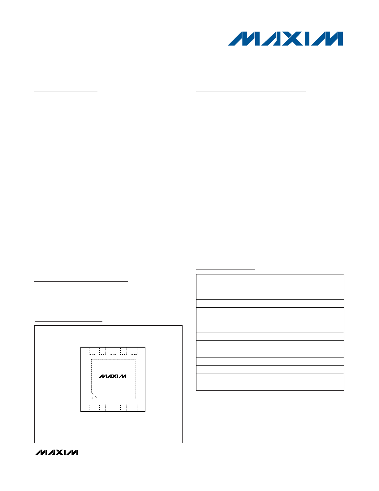
Pin Configurations
Ordering Information
19-1053; Rev 1; 3/08
For pricing, delivery, and ordering information, please contact Maxim Direct at 1-888-629-4642,
or visit Maxim’s website at www.maxim-ic.com.
Note: All devices are specified over the -40°C to +125°C operating
temperature range.
+
Denotes a lead-free package.
*
Future product—contact factory for availability.
**
EP = Exposed pad. T = Tape and reel.
See the Selector Guide at the end of the data sheet.
Pin Configurations continued at end of data sheet.
Block Diagrams appear at end of data sheet.
PART
PKG
CODE
TOP
MARK
ATX
ATY
—
—
ATZ
AUA
AUB
AUC
—
—
—
—
TOP VIEW
REG
10 87
1
FB/SET
*EP = EXPOSED PAD.
P_OUT
DRVV
9
MAX15024
EP*
CC
N_OUT
3425
IN+
GND
TDFN
PGNDIN-
6
PIN-PACKAGE
MAX15024AATB+T 10 TDFN-EP** T1033-1
MAX15024BATB+T 10 TDFN-EP** T1033-1
MAX15024CATB+T* 10 TDFN-EP** T1033-1
MAX15024DATB+T* 10 TDFN-EP** T1033-1
MAX15025AATB+T 10 TDFN-EP** T1033-1
MAX15025BATB+T 10 TDFN-EP** T1033-1
MAX15025CATB+T 10 TDFN-EP** T1033-1
MAX15025DATB+T 10 TDFN-EP** T1033-1
MAX15025EATB+T* 10 TDFN-EP** T1033-1
MAX15025FATB+T* 10 TDFN-EP** T1033-1
MAX15025GATB+T* 10 TDFN-EP** T1033-1
MAX15025HATB+T* 10 TDFN-EP** T1033-1
Page 2
MAX15024/MAX15025
Single/Dual, 16ns, High Sink/Source
Current Gate Drivers
2 _______________________________________________________________________________________
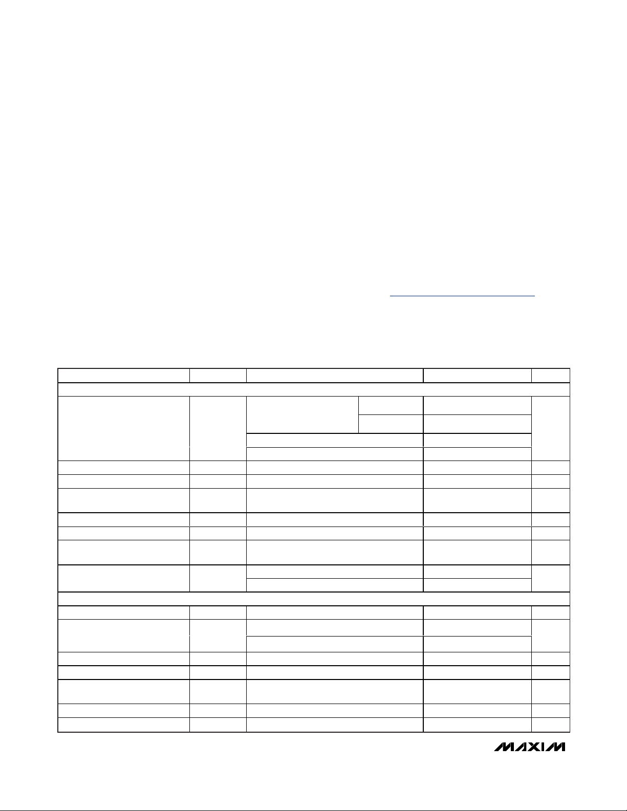
ABSOLUTE MAXIMUM RATINGS
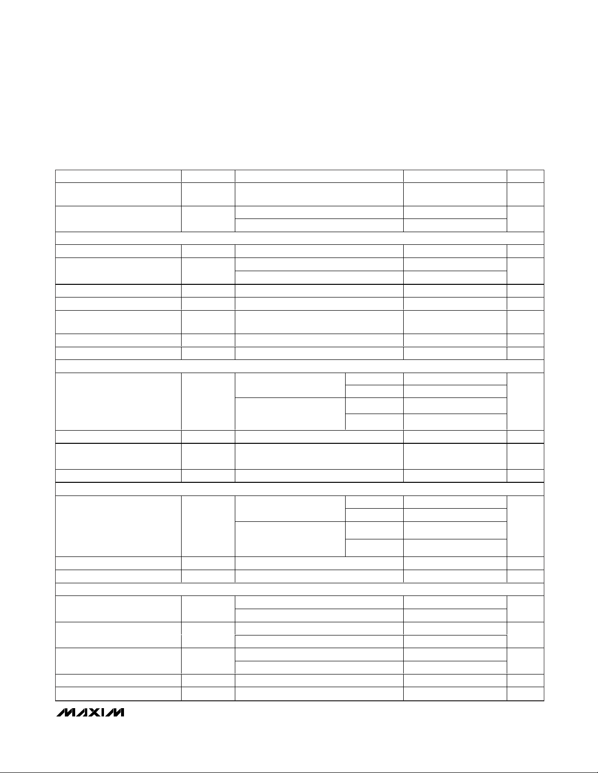
MAX15024 ELECTRICAL CHARACTERISTICS
(VCC= V
DRV
= V
REG
= 10V, FB/SET = GND, TA= TJ= -40°C to +125°C, unless otherwise noted. Typical values are at TA= TJ=
+ 25°C). (Note 2)
Stresses beyond those listed under “Absolute Maximum Ratings” may cause permanent damage to the device. These are stress ratings only, and functional
operation of the device at these or any other conditions beyond those indicated in the operational sections of the specifications is not implied. Exposure to
absolute maximum rating conditions for extended periods may affect device reliability.
VCCto GND............................................................-0.3V to +30V
REG to GND..............-0.3V to the lower of +22V or (V
CC
+ 0.3V)
DRV to PGND .........................................................-0.3V to +22V
IN_ ..........................................................................-0.3V to +22V
FB/SET to GND.........................................................-0.3V to +6V
P_OUT to DRV ........................................................-22V to +0.3V
N_OUT to PGND.....................................................-0.3V to +22V
OUT1, OUT2 to PGND ..............................-0.3V to (V
DRV
+ 0.3V)
PGND to GND .......................................................-0.3V to +0.3V
P_OUT, N_OUT Continuous Source/Sink Current* .......... 200mA
OUT1, OUT2 Continuous Source/Sink Current*................200mA
Continuous Power Dissipation (T
A
= +70°C)
10-Pin TDFN, Single-Layer Board
(derate 18.5mW/°C above +70°C)...........................1481.5mW
Junction-to-Case Thermal Resistance (Note 1) ..............8.5°C/W
10-Pin TDFN, Multilayer Board
(derate 24.4mW/°C above +70°C)...........................1951.2mW
Junction-to-Case Thermal Resistance (Note 1) ..............8.5°C/W
Operating Temperature Range .........................-40°C to +125°C
Junction Temperature......................................................+150°C
Storage Temperature Range .............................-65°C to +150°C
Lead Temperature (soldering, 10s) .................................+300°C
*
Continuous output current is limited by the power dissipation of the package.
Note 1: Package thermal resistances were obtained using the method described in JEDEC specification JESD51-7, using a four-
layer board. For detailed information on package thermal considerations, see www.maxim-ic.com/thermal.tutorial
.
SYSTEM SPECIFICATIONS
Input Voltage Range V
V
DRV
Quiescent Supply Current IN_ = VCC or GND 700 1350 µA
Quiescent Supply Current
Under UVLO Condition
Switching Supply Current Switching at 250kHz, CL = 0 1.5 3.0 mA
VCC Undervoltage Lockout UVLO_ VCCV
VCC Undervoltage-Lockout
Hysteresis
VCC Undervoltage Lockout to
Output Delay
REG REGULATOR (VCC = 12V, REG = V
Output Voltage V
Dropout Voltage VR_
Load Regulation VCC = 12V, I
Line Regulation 12V < VCC < 28V 10 mV
FB/SET Reference Voltage
FB/SET Threshold VFB falling 220 mV
FB/SET Input Leakage Current VFB = 4.5V (Note 3) -125 +125 nA
PARAMETER SYMBOL CONDITIONS MIN TYP MAX UNITS
Turn-On Voltage V
VCC powered only, V
V
DRV
CC
DRV_ONVCC
REG
minimum 1µF to GND
VCC = V
V
CC
IN_ = V
CC
V
CC
V
CC
, CL = 1µF, FB/SET = GND)
DRV
12V < VCC < 28V, 0 < I
VCC = 6.5V, I
DO
VCC = 4.5V, I
External resistive divider connected at
FB/SET
decoupled with
= V
REG
DRV
= V
= V
REG
DRV
= V
= 10V, IN+ = VCC, IN- = GND 1.7 2.3 V
REG
or GND 250 µA
CC
rising 3.0 3.4 3.8 V
rising 100
falling 2
LOAD
LOAD
LOAD
=
REG
(MAX15024D) 6.5 18.0
(MAX15024C) 4.5 18.0
= 100mA 0.4 0.9
= 50mA 0.2 0.5
= 0 to 100mA 1 %
MAX15024B/D 6.5 28.0
MAX15024A/C 4.5 28.0
< 10mA
LOAD
300 mV
91011 V
1.10 1.23 1.35 V
V
µs
V
Page 3
MAX15024/MAX15025
Single/Dual, 16ns, High Sink/Source
Current Gate Drivers
_______________________________________________________________________________________ 3
MAX15024 ELECTRICAL CHARACTERISTICS (continued)
(VCC= V
DRV
= V
REG
= 10V, FB/SET = GND, TA= TJ= -40°C to +125°C, unless otherwise noted. Typical values are at TA= TJ=
+ 25°C). (Note 2)
DRIVER OUTPUT (SINK)
Driver Output Resistance R
Peak Output Current I
Maximum Load Capacitance
Latchup Robustness 500 mA
DRIVER OUTPUT (SOURCE)
Driver Output Resistance R
Peak Output Current I
Latchup Robustness 500 mA
LOGIC INPUTS
Logic 1 Input Voltage V
Logic 0 Input Voltage V
Logic Input Hysteresis
Logic Input Current Leakage VIN = 18V or GND -75 0.01 +75 µA
Input Capacitance 10 pF
SWITCHING CHARACTERISTICS FOR VCC = V
(see Figure 1)
Rise Time t
Turn-On Delay Time t
Turn-Off Delay Time t
Mismatch Propagation Delays
from Inverting and Noninverting
Inputs to Output
PARAMETER SYMBOL CONDITIONS MIN TYP MAX UNITS
TA = +25°C 0.45 0.60
T
= +125°C 0.625 0.850
A
TA = +25°C 0.50 0.65
ON-N
VCC = V
REG
= V
sinking 100mA
VCC = V
REG
= V
DRV
DRV
= 10V,
= 4.5V,
sinking 100mA
T
= +125°C 0.7 0.9
A
2
≤ 20µJ,
200 nF
TA = +25°C 0.875 1.500
T
= +125°C 1.2 2.0
A
TA = +25°C 0.95 1.65
PK-N
ON-P
(MAX15024C/D)
V
= 10V 8 A
N_OUT
SOA condition: C
for V
VCC = V
DRV
= 10V
REG
= V
L
DRV
x V
= 10V,
DRV
sourcing 100mA
VCC = V
REG
= V
DRV
= 4.5V,
sourcing 100mA
T
= +125°C 1.25 2.20
A
PK-P
IH
IL
(MAX15024C/D)
V
= 0V 4 A
P_OUT
MAX15024A/C 2.0
MAX15024B/D 4.25
MAX15024A/C 0.8
MAX15024B/D 2
MAX15024A/C 0.4
MAX15024B/D 1
= 10V, P_OUT AND N_OUT ARE CONNECTED TOGETHER
REG
= 1nF 3
= 5nF 12
= 10nF 24
= 1nF 3
= 5nF 8Fall Time t
= 10nF 16
= 1nF (Note 3) 8 16 32 ns
= 1nF (Note 3) 8 16 32 ns
= 1nF 1 ns
R
F
D-ON
D-OFF
DRV
C
LOAD
C
LOAD
C
LOAD
C
LOAD
C
LOAD
C
LOAD
C
LOAD
C
LOAD
C
LOAD
= V
Ω
Ω
V
V
V
ns
ns
Page 4
MAX15024/MAX15025
Single/Dual, 16ns, High Sink/Source
Current Gate Drivers
4 _______________________________________________________________________________________
MAX15024 ELECTRICAL CHARACTERISTICS (continued)
(VCC= V
DRV
= V
REG
= 10V, FB/SET = GND, TA= TJ= -40°C to +125°C, unless otherwise noted. Typical values are at TA= TJ=
+ 25°C). (Note 2)
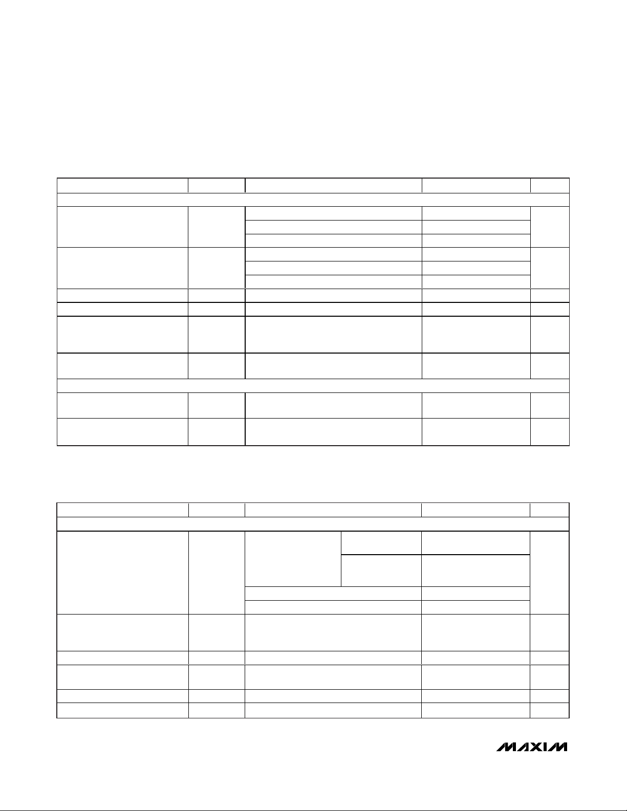
MAX15025 ELECTRICAL CHARACTERISTICS
(VCC= V
DRV
= V
REG
= 10V, FB/SET = GND, TA= TJ= -40°C to +125°C, unless otherwise noted. Typical values are at TA= TJ=
+25°C). (Note 2)
SWITCHING CHARACTERISTICS FOR VCC = V
Rise Time t
Fall Time t
Turn-On Delay Time t
Turn-Off Delay Time t
Mismatch Propagation Delays
from Inverting and Noninverting
Inputs to Output
Minimum Input Pulse Width that
Changes the Output
THERMAL CHARACTERISTICS
Thermal-Shutdown
Temperature
Thermal-Shutdown
Temperature Hysteresis
PARAMETER SYMBOL CONDITIONS MIN TYP MAX UNITS
R
F
D-ON
D-OFF
t
PW
= V
DRV
C
LOAD
C
LOAD
C
LOAD
C
LOAD
C
LOAD
C
LOAD
C
LOAD
C
LOAD
C
LOAD
Temperature rising +160 °C
= 4.5V (see Figure 1) (MAX15024C/D)
REG
= 1nF 3
= 5nF 11
= 10nF 22
= 1nF 2.5
= 5nF 8
= 10nF 16
= 1nF 18 ns
= 1nF 18 ns
= 1nF 2 ns
ns
ns
15 ns
15 °C
SYSTEM SPECIFICATIONS
Input Voltage Range V
V
DRV
Quiescent Supply Current IN_ = VCC or GND 700 1350 µA
Quiescent Supply Current
Under UVLO Condition
Switching Supply Current Switching at 250kHz, CL = 0 1.5 3.0 mA
VCC Undervoltage Lockout UVLO_ VCCV
PARAMETER SYMBOL CONDITIONS MIN TYP MAX UNITS
Turn-On Voltage V
CC
DRV_ON
VCC powered only,
V
= V
REG
decoupled with
minimum 1µF
to GND
VCC = V
VCC = V
VCC = V
(M AX 15025A/B/E /F) or G N D for
( M AX 15025C /D /G/H )
IN_ = V
DRV
= V
REG
DRV
= V
REG
DRV
= 10V, IN1 = VCC, IN2 = V
REG
or GND 250 µA
CC
rising 3.0 3.4 3.8 V
CC
MAX15025B/D/F/H 6.5 28
MAX15025A/C/E/G 4.5 28
(MAX15025F/H) 6.5 18.0
(MAX15025E/G) 4.5 18.0
CC
1.7 2.3 V
V
Page 5
MAX15024/MAX15025
Single/Dual, 16ns, High Sink/Source
Current Gate Drivers
_______________________________________________________________________________________ 5
MAX15025 ELECTRICAL CHARACTERISTICS (continued)
(VCC= V
DRV
= V
REG
= 10V, FB/SET = GND, TA= TJ= -40°C to +125°C, unless otherwise noted. Typical values are at TA= TJ=
+25°C). (Note 2)
VCC Undervoltage-Lockout
Hysteresis
VCC Undervoltage Lockout to
Output Delay
REG REGULATOR (VCC = 12V, V
Output Voltage V
Dropout Voltage VR_
Load Regulation VCC = 12V, I
Line Regulation 12V < VCC < 28V 10 mV
FB/SET Reference Voltage
FB/SET Threshold VFB rising 220 mV
FB/SET Input Leakage Current VFB = 4.5V -125 +125 nA
DRIVER OUTPUT SINK
Driver Output Resistance R
Peak Output Current I
Maximum Load Capacitance
Latchup Robustness 500 mA
DRIVER OUTPUT SOURCE
Driver Output Resistance R
Peak Output Current I
Latchup Robustness 500 mA
LOGIC INPUTS
Logic 1 Input Voltage V
Logic 0 Input Voltage V
Logic Input Hysteresis
Logic Input Current Leakage VIN = 18V or GND -75 +0.01 +75 µA
Input Capacitance 10 pF
PARAMETER SYMBOL CONDITIONS MIN TYP MAX UNITS
300 mV
V
rising 100
CC
falling 2
V
CC
REG
= V
, CL = 1µF, FB/SET = GND)
DRV
REG
12V < VCC < 28V, 0 < I
VCC = 6.5V, I
DO
VCC = 4.5V, I
External resistive divider connected at
FB/SET
VCC = V
sinking 100mA
ON-N
VCC = V
REG
REG
< 10mA 9 10 11 V
LOAD
= 100mA 0.4 0.9
LOAD
= 50mA 0.2 0.5
LOAD
= 0 to 100mA 1 %
LOAD
1.10 1.23 1.35 V
= V
= V
DRV
DRV
= 10V,
= 4.5V,
TA = +25°C 1.0 1.6
= +125°C 1.25 2.10
T
A
TA = +25°C 1.10 1.65
sinking 100mA
T
= +125°C 1.5 2.2
A
2
≤ 20µJ,
100 nF
TA = +25°C 1.75 2.50
T
= +125°C 2.25 3.50
A
TA = +25°C 1.85 2.60
PK-N
ON-P
(MAX15025E/F/G/H)
V
= 10V 4 A
OUT_
SOA condition: C
DRV
= 10V
REG
for V
VCC = V
= V
L
DRV
x V
= 10V,
DRV
sourcing 100mA
VCC = V
REG
= V
DRV
= 4.5V,
sourcing 100mA
T
= +125°C 2.50 3.75
A
PK-P
IH
IL
(MAX15025E/F/G/H)
V
= 0V 2 A
OUT_
MAX15025A/C/E/G 2.0
MAX15025B/D/F/H 4.25
MAX15025A/C/E/G 0.8
MAX15025B/D/F/H 2
MAX15025A/C/E/G 0.4
MAX15025B/D/F/H 1
µs
V
Ω
Ω
V
V
V
Page 6

MAX15024/MAX15025
Single/Dual, 16ns, High Sink/Source
Current Gate Drivers
6 _______________________________________________________________________________________
MAX15025 ELECTRICAL CHARACTERISTICS (continued)
(VCC= V
DRV
= V
REG
= 10V, FB/SET = GND, TA= TJ= -40°C to +125°C, unless otherwise noted. Typical values are at TA= TJ=
+25°C). (Note 2)
Note 2: All devices are 100% production tested at TA= +25°C. Limits over temperature are guaranteed by design.
Note 3: Design guaranteed by bench characterization. Limits are not production tested.
SWITCHING CHARACTERISTICS FOR VCC = V
Fall Time t
Turn-On Delay Time t
Turn-Off Delay Time t
Mismatch Propagation Delays
Between 2 Channels
SWITCHING CHARACTERISTICS FOR VCC = V
Rise Time t
Fall Time t
Turn-On Delay Time t
Turn-Off Delay Time t
Mismatch Propagation Delays
Between 2 Channels
Minimum Input Pulse Width that
Changes the Output
THERMAL CHARACTERISTICS
Thermal-Shutdown Temperature Temperature rising +160 °C
Thermal-Shutdown Temperature
Hysteresis
PARAMETER SYMBOL CONDITIONS MIN TYP MAX UNITS
= V
= 10V (see Figure 1)
REG
= 1nF 6
= 5nF 24Rise Time t
= 10nF 48
= 1nF 5
= 5nF 16
= 10nF 32
= 1nF (Note 3) 8 16 32 ns
= 1nF (Note 3) 8 16 32 ns
= 1nF 1 ns
= V
= 4.5V (see Figure 1) (MAX15025E/F/G/H)
REG
= 1nF 5
= 5nF 20
= 10nF 42
= 1nF 4
= 5nF 15
= 10nF 30
= 1nF 18 ns
= 1nF 18 ns
= 1nF 2 ns
15 ns
R
F
D-ON
D-OFF
R
F
D-ON
D-OFF
t
PW
DRV
C
LOAD
C
LOAD
C
LOAD
C
LOAD
C
LOAD
C
LOAD
C
LOAD
C
LOAD
C
LOAD
DRV
C
LOAD
C
LOAD
C
LOAD
C
LOAD
C
LOAD
C
LOAD
C
LOAD
C
LOAD
C
LOAD
15 °C
ns
ns
ns
ns
Page 7

MAX15024/MAX15025
Single/Dual, 16ns, High Sink/Source
Current Gate Drivers
_______________________________________________________________________________________
7
Typical Operating Characteristics
(TA = +25°C, unless otherwise noted.)
RISE TIME vs. SUPPLY VOLTAGE
FALL TIME vs. SUPPLY VOLTAGE
(DUAL DRIVER WITH 5nF LOAD)
40
TA = +125°C
30
20
RISE TIME (ns)
10
TA = -40°C
0
10 20
TA = +85°C
TA = 0°C
SUPPLY VOLTAGE (V)
TA = +25°C
MAX15025
MAX15024/25 toc01
191817161514131211
30
MAX15025
25
TA = +125°C
20
FALL TIME (ns)
15
TA = -40°C
10
10 20
SUPPLY CURRENT vs. SUPPLY VOLTAGE
(PROGRAMMED EXTERNALLY TO 5V)
2500
2000
1500
1000
SUPPLY CURRENT (μA)
500
1MHz
500kHz
100kHz
0
020
SUPPLY VOLTAGE (V)
75kHz
40kHz
MAX15024/25 toc04
18161412108642
30
VCC = V
24
18
12
SUPPLY CURRENT (mA)
6
0
0 10,000
(WITH 5nF LOAD)
TA = +85°C
TA = +25°C
TA = 0°C
SUPPLY VOLTAGE (V)
SUPPLY CURRENT
vs. LOAD CAPACITANCE
= V
= 10V
REG
DRV
SWITCHING
250kHz
NOT SWITCHING
LOAD CAPACITANCE (nF)
PROPAGATION DELAY TIME
vs. TEMPERATURE (1nF LOAD)
18
16
MAX15024/25 toc02
14
12
10
PROPAGATION DELAY TIME (ns)
8
1800
1600
1400
MAX15024/25 toc05
1200
1000
800
600
SUPPLY CURRENT (μA)
400
200
6
-60 140
VCC = V
0
-40 120
18161412
8000600040002000
RISING
FALLING
TEMPERATURE (°C)
SUPPLY CURRENT
vs. TEMPERATURE
= V
= 10V
REG
DRV
SWITCHING
250kHz
NOT SWITCHING
TEMPERATURE (°C)
MAX15024/25 toc03
120100806040200-20-40
MAX15024/25 toc06
80400
INPUT THRESHOLD VOLTAGE
vs. SUPPLY VOLTAGE (TTL)
3.0
2.5
2.0
1.5
1.0
INPUT THRESHOLD VOLTAGE (V)
0.5
0
420
RISING
FALLING
16128
SUPPLY VOLTAGE (V)
MAX15024/25 toc07
1600
1400
1200
1000
800
600
SUPPLY CURRENT (μA)
400
200
00
06
SUPPLY CURRENT
vs. LOGIC IN
INPUT
LOW TO HIGH
INPUT
HIGH TO LOW
INPUT VOLTAGE (V)
LOGIC INPUT VOLTAGE vs. OUTPUT VOLTAGE
(5nF RISING)
MAX15024/25 toc08
541 2 3
20ns/div
MAX15024/25 toc09
MAX15025
IN_
1V/div
OUT_
5V/div
Page 8

MAX15024/MAX15025
Single/Dual, 16ns, High Sink/Source
Current Gate Drivers
8 _______________________________________________________________________________________
Typical Operating Characteristics (continued)
(TA = +25°C, unless otherwise noted.)
LOGIC INPUT VOLTAGE vs. OUTPUT VOLTAGE
(5nF FALLING)
20ns/div
PROPAGATION DELAY MISMATCH
MAX15024/25 toc10
MAX15025
IN_
1V/div
OUT_
5V/div
vs. TEMPERATURE
3.0
2.5
2.0
1.5
1.0
0.5
PROPAGATION DELAY BETWEEN CHANNELS (ns)
0
-40 120
TEMPERATURE (°C)
80400
MAX15024/25 toc13
LOGIC INPUT VOLTAGE vs. OUTPUT VOLTAGE
(PROGRAMMED EXTERNALLY TO 5.04V)
5.3
5.2
5.1
(V)
5.0
REG
V
4.9
4.8
4.7
530
(10nF RISING)
20ns/div
LINE REGULATION OF V
SUPPLY VOLTAGE
MAX15024/25 toc11
MAX15025
REG
25201510
IN_
1V/div
OUT_
5V/div
MAX15024/25 toc14
LOGIC INPUT VOLTAGE vs. OUTPUT VOLTAGE
(10nF FALLING)
20ns/div
LOAD REGULATION OF V
11.0
10.5
(V)
10.0
REG
V
9.5
9.0
0 200
LOAD CURRENT (mA)
MAX15024/25 toc12
MAX15025
REG
IN_
1V/div
OUT_
5V/div
MAX15024/25 toc15
18016014012010080604020
FB/SET VOLTAGE
vs. TEMPERATURE
1.240
1.238
1.236
1.234
FB/SET VOLTAGE (V)
1.232
1.230
0120
TEMPERATURE (°C)
MAX15024/25 toc16
10080604020
20
15
10
FB/SET CURRENT (nA)
5
0
0 120
FB/SET CURRENT
vs. TEMPERATURE
TEMPERATURE (°C)
MAX15024/25 toc17
10080604020
Page 9

MAX15024/MAX15025
Single/Dual, 16ns, High Sink/Source
Current Gate Drivers
_______________________________________________________________________________________ 9
Pin Description
PIN
MAX15025A
MAX15024
1 1 1 FB/SET
22 2V
3 3 3 GND Signal Ground
4 — — IN+ Driver Noninverting Logic Input. Connect to VCC when not used.
— 4 4 IN1 Driver 1 Noninverting Logic Input
5 — — IN- Driver Inverting Logic Input. Connect to GND when not used.
— 5 — IN2 Driver 2 Noninverting Logic Input
—— 5IN2 Driver 2 Inverting Logic Input
6 6 6 PGND
7 — — N_OUT
— 7 7 OUT2 Driver 2 Output
8 — — P_OUT
— 8 8 OUT1 Driver 1 Output
9 9 9 DRV
MAX15025B
MAX15025E
MAX15025F
MAX15025C
MAX15025D
MAX15025G
MAX15025H
NAME FUNCTION
LDO Regulator Output Set. Feedback for V
Connect FB/SET to GND for a fixed 10V output REG. Connect FB/SET to a
resistor ladder to set V
Power-Supply Input. Bypass to GND with a low-ESR ceramic capacitor of
1µF. Input of the internal housekeeping regulator and of the main REG
CC
regulator.
Power Ground. Sink current return. Source of the internal pulldown
n-channel transistor.
Sink Output. Open-drain n-channel output. N_OUT sinks current for power
MOSFET turn-off.
Source Output. Pullup p-channel output (open drain). Sources current for
power MOSFET turn-on.
Output Driver Supply Voltage. Decouple DRV with a low ESR > 0.1µF
ceramic capacitor to PGND placed in close proximity to the device. DRV
can be powered independently from REG. Connect DRV, REG, and V
together when there is no need for special DRV supply sequencing and
the power-MOSFET gate voltage does not need to be regulated or limited.
REG
.
adjustment (V
REG
> 200mV).
FB
CC
Voltage Regulator Output. Connect to DRV for driving the power MOSFET
10 10 10 REG
—— —EP
with regulated V
ceramic capacitor to GND placed in close proximity to the device to
ensure regulator stability.
Exposed Pad. Internally connected to GND. Connect to GND plane or
thermal pad and use multiple vias to a solid copper area on the bottom of
the PCB.
amplitude. Bypass with a low-ESR 1µF (minimum)
GS
Page 10

MAX15024/MAX15025
Single/Dual, 16ns, High Sink/Source
Current Gate Drivers
10 ______________________________________________________________________________________
Detailed Description
The MAX15024 single gate driver’s internal source and
sink transistor outputs are brought out of the IC to independent outputs allowing control of the external
MOSFET’s rise and fall time. The MAX15024 single
gate driver is capable of sinking an 8A peak current
and sourcing a 4A peak current. The MAX15025 dual
gate drivers are capable of sinking a 4A peak current
and sourcing a 2A peak current.
An integrated adjustable low-dropout linear voltage
regulator (LDO) provides gate drive amplitude control
and optimization. The single gate-driver propagation
delay time is minimized and matched between the
inverting and noninverting inputs. The dual gate-driver
propagation delay is matched between channels.
The MAX15024 has a dual input (IN+ and IN-), allows
the use of an inverting or noninverting input, and is
offered in TTL or CMOS-logic standards. The
MAX15025 is offered with configurations of inverting
and noninverting inputs with TTL or CMOS standards
(see the
Selector Guide
).
The MAX15024A/B and MAX15025A/B/C/D can be powered using VCConly, whereas the MAX15024C/D and
MAX15025E/F/G/H can be used in two configurations:
•VCCpowered only
•VCC, REG, and DRV are connected together
LDO Voltage Regulator Feedback Control
The MAX15024/MAX15025 include an internal LDO
designed to deliver a stable reference voltage for use
as a supply voltage for the internal MOSFET gate drivers. Connect the LDO feedback FB/SET to GND to set
V
REG
to a stable 10V. Connect FB/SET to a resistor-
divider between V
REG
and GND to set V
REG
:
V
REG
= V
FB/SET
x (1 + R2 / R1) (see Figure 2)
VCCUndervoltage Lockout
When VCCis below the UVLO threshold, the internal nchannel transistor is ON and the internal p-channel transistor is OFF, holding the output at GND independent of
the state of the inputs so that the external MOSFETs
remain OFF in the UVLO condition. The UVLO threshold is
3.5V (typ) with 200mV (typ) hysteresis to avoid chattering.
When the device is operated at very low temperatures
and below the UVLO threshold, the driver output could
go high impedance. In this case, it is recommended
adding a 10kΩ resistor to PGND to discharge the gate
of the external MOSFET (see Figures 4 and 5).
Input Control
The MAX15024 features inverting and noninverting
input terminals. These inputs provide for flexibility of
design and use. Connect IN+ to VCCwhen using IN- as
an inverting input. Connect IN- to GND when using IN+
as a noninverting input.
Shoot-Through Protection
The MAX15024/MAX15025 provide protection that
avoids any cross-conduction between the internal pchannel and n-channel devices. It also eliminates shootthrough, thus reducing the quiescent supply current.
Exposed Pad (EP)
The MAX15024/MAX15025 include an exposed pad
allowing greater heat dissipation from the internal die to
the outside environment. Solder the exposed pad carefully to GND or thermal pad to enhance the thermal
performance.
Applications Information
Supply Bypassing, Device Grounding,
and Placement
Ample supply bypassing and device grounding are
extremely important because when large external
capacitive loads are driven, the peak current at the
V
DRV
pin can approach 4A, while at the PGND pin, the
peak current can approach 8A. V
DRV
drops and
ground shifts are forms of negative feedback for inverters and, if excessive, can cause multiple switching
when the inverting input is used and the input slew rate
is low. The device driving the input should be referenced to the MAX15024/MAX15025 GND. Ground
shifts due to insufficient device grounding can disturb
other circuits sharing the same AC ground return path.
Any series inductance in the V
DRV
, OUT_, and/or PGND
paths can cause oscillations due to the very high di/dt
that results when the MAX15024/MAX15025 are
switched with any capacitive load. A 0.1µF or larger
value ceramic capacitor is recommended for bypassing V
DRV
to GND and should be placed as close to the
pins as possible. When driving very large loads
(> 10nF) at minimum rise time, 10µF or more of parallel
storage capacitance is recommended. A ground plane
is highly recommended to minimize ground return resistance and series inductance. Care should be taken to
place the MAX15024/MAX15025 as close as possible to
the external MOSFET being driven to further minimize
board inductance and AC path resistance.
Page 11

Power Dissipation
Power dissipation of the MAX15024/MAX15025 consists of three components: the quiescent current,
capacitive charge and discharge of internal nodes, and
the output current (either capacitive or resistive load).
The sum of these components must be kept below the
maximum power-dissipation limit. The quiescent current is 700µA typ. The current required to charge and
discharge the internal nodes is frequency dependent
(see the
Typical Operating Characteristics
). The
MAX15024/MAX15025 power dissipation when driving
a ground-referenced resistive load is:
P = D x R
ON(MAX)
x I
LOAD
2
where D is the fraction of the period the MAX15024/
MAX15025s’ output pulls high, R
ON(MAX)
is the maximum on-resistance of the device with the output high
(p-channel), and I
LOAD
is the output load current of the
MAX15024/MAX15025. For capacitive loads, the power
dissipation for each driver is:
P = C
LOAD
x V
DRV
2
x FREQ
where C
LOAD
is the capacitive load, V
DRV
is the driver
supply voltage, and FREQ is the switching frequency.
Layout Information
The MAX15024/MAX15025 MOSFET drivers source and
sink large currents to create very fast rise and fall edges
at the gate of the switching MOSFET. The high di/dt can
cause unacceptable ringing if the trace lengths and
impedances are not well controlled. The following
printed-circuit board (PCB) layout guidelines are recommended when designing with the MAX15024/MAX15025:
• Place one or more 1µF decoupling ceramic capacitor(s) from V
DRV
to PGND as close to the device as
possible. At least one storage capacitor of 10µF (min)
should be located on the PCB with a low resistance
path to the V
CC
pin of the MAX15024/MAX15025.
• There are two AC current loops formed between the
device and the gate of the MOSFET being driven.
The MOSFET looks like a large capacitance from
gate to source when the gate is being pulled low.
The active current loop is from MOSFET gate to
OUT_ of the MAX15024/MAX15025 to PGND of the
MAX15024/MAX15025, and to the source of the
MOSFET. When the gate of the MOSFET is being
pulled high, the active current loop is from the V
DD
terminal of the V
DRV
terminal of decoupling capaci-
tor, to the V
DRV
of the MAX15024/MAX15025, to the
OUT_ of the MAX15024/MAX15025, to the MOSFET
gate, to the MOSFET source, and to the negative terminal of the decoupling capacitor. Both charging
current loop and discharging current loop are important. It is important to minimize the physical distance
and the impedance in these AC current paths.
• Keep the device as close as possible to the MOSFET.
• In the multilayer PCB, the inner layers should consist
of a GND plane containing the discharging and
charging current loops.
MAX15024/MAX15025
Single/Dual, 16ns, High Sink/Source
Current Gate Drivers
______________________________________________________________________________________ 11
Figure 1. Timing Diagram
IN+
P_OUT AND
N_OUT CONNECTED
TOGETHER
OR OUT1/OUT2
V
IH
V
IL
90%
10%
t
D-OFF
t
F
t
D-ON
t
R
Page 12

MAX15024/MAX15025
Single/Dual, 16ns, High Sink/Source
Current Gate Drivers
12 ______________________________________________________________________________________
Typical Operating Circuits
Figure 2. Connect FB/SET to GND for V
REG
= 10V (Connect EP
to GND)
Figure 3. Operation Using a Different Supply Rail for DRV
(Connect EP to GND)
Figure 4. Operation Using a VCC= DRV = REG (Connect EP
to GND)
Figure 5. Connect FB/SET to GND for V
REG
= 10V (Connect EP
to GND)
V
CC
(UP TO 18V)
V
CC
REG
FB/SET
GND
MAX15024
V
CC
(UP TO 28V)
REG
DRV
R2
R1
FB/SET
V
CC
MAX15024
P_OUT
N_OUT
PGND
DRV
P_OUT
N_OUT
< 18V
V
DRV
C1
GND
IN-
IN+
V
CC
(UP TO 28V)
V
CC
REG
MAX15024C/D
FB/SET
GND
IN-
IN+
DRV
P_OUT
N_OUT
PGND
IN-
IN+
PGND
REG
DRV
V
CC
(UP TO 28V)
R2
R1
FB/SET
V
CC
GND
IN1
IN2
MAX15025
OUT1
OUT2
PGND
Page 13

MAX15024/MAX15025
Single/Dual, 16ns, High Sink/Source
Current Gate Drivers
______________________________________________________________________________________ 13
Block Diagrams
V
IN+
GND
CC
UVLO
IN_ LOGIC
LEVEL SHIFT-UP
IN-
IN_ LOGIC
LEVEL SHIFT-UP
LDO
PREDRIVER
PREDRIVER
MAX15024A
MAX15024B
REG
DRV
VDRV
P
P_OUT
N_OUT
N
PGND
V
FB/SET
IN1
IN2
GND
CC
UVLO
IN_ LOGIC
LEVEL SHIFT-UP
IN_ LOGIC
LEVEL SHIFT-UP
IN_ LOGIC
LEVEL SHIFT-UP
IN_ LOGIC
LEVEL SHIFT-UP
LDO
PREDRIVER
PREDRIVER
PREDRIVER
PREDRIVER
P
N
REG
DRV
P
OUT1
N
OUT2
PGND
MAX15025
Page 14

MAX15024/MAX15025
Single/Dual, 16ns, High Sink/Source
Current Gate Drivers
14 ______________________________________________________________________________________
Selector Guide
Note: All devices operate in a -40°C to +125°C temperature range and come in a 10-pin TDFN package.
PART
MAX15024AATB+ 1 8A/4A Complementary TTL ATX ✔ —
MAX15024BATB+ 1 8A/4A Complementary CMOS ATY ✔ —
MAX15024CATB+ 1 8A/4A Complementary TTL — ✔✔
MAX15024DATB+ 1 8A/4A Complementary CMOS — ✔✔
MAX15025AATB+ 2 4A/2A Noninverting TTL ATZ ✔ —
MAX15025BATB+ 2 4A/2A Noninverting CMOS AUA ✔ —
MAX15025CATB+ 2 4A/2A
MAX15025DATB+ 2 4A/2A
MAX15025EATB+ 2 4A/2A Noninverting TTL — ✔✔
MAX15025FATB+ 2 4A/2A Noninverting CMOS — ✔✔
MAX15025GATB+ 2 4A/2A
MAX15025HATB+ 2 4A/2A
NO. OF
CHANNELS
PEAK
CURRENTS
(SINK/SOURCE)
INPUTS
Noninverting (1)/
Inverting (2)
Noninverting (1)/
Inverting (2)
Noninverting (1)/
Inverting (2)
Noninverting (1)/
Inverting (2)
LOGIC
LEVELS
TTL AUB ✔ —
CMOS AUC ✔ —
TTL — ✔✔
CMOS — ✔✔
TOP
MARK
-
V
CC
POWERED
ONLY
= V
V
CC
V
DRV
REG
=
Page 15

MAX15024/MAX15025
Single/Dual, 16ns, High Sink/Source
Current Gate Drivers
______________________________________________________________________________________ 15
Chip Information
PROCESS: BiCMOS
EP
TOP VIEW
10 87
REG
OUT1
OUT2
FB/SET
GND
IN1
MAX15025A/E
MAX15025B/F
9
DRVV
CC
6
13425
PGNDIN2
TDFN
EP
10 87
REG
OUT1
OUT2
FB/SET
GND
IN1
MAX15025C/G
MAX15025D/H
9
DRVV
CC
6
13425
PGNDIN2
TDFN
Pin Configurations (continued)
Package Information
For the latest package outline information, go to
www.maxim-ic.com/packages
.
PACKAGE TYPE PACKAGE CODE DOCUMENT NO.
10 TDFN T1033-1
21-0137
Page 16

MAX15024/MAX15025
Single/Dual, 16ns, High Sink/Source
Current Gate Drivers
Maxim cannot assume responsibility for use of any circuitry other than circuitry entirely embodied in a Maxim product. No circuit patent licenses are
implied. Maxim reserves the right to change the circuitry and specifications without notice at any time.
16
____________________Maxim Integrated Products, 120 San Gabriel Drive, Sunnyvale, CA 94086 408-737-7600
© 2008 Maxim Integrated Products is a registered trademark of Maxim Integrated Products, Inc.
Revision History
REVISION
NUMBER
0 10/07 Initial release —
1 3/08
REVISION
DATE
Updated Ordering Information and Electrical Characteristics tables and
revised Block Diagram.
DESCRIPTION
PAGES
CHANGED
1–6, 9, 13
 Loading...