

Page 1
General Description
The MAX15023 dual, synchronous step-down controller
operates from a 5.5V to 28V or 5V ±10% input voltage
range and generates two independent output voltages.
Each output is adjustable from 85% of the input voltage
down to 0.6V and supports loads of 12A or higher. Input
voltage ripple and total RMS input ripple current are
reduced by interleaved 180° out-of-phase operation.
The MAX15023 offers the ability to adjust the switching
frequency from 200kHz to 1MHz with an external resistor.
The MAX15023’s adaptive synchronous rectification eliminates the need for external freewheeling Schottky diodes.
The device also utilizes the external low-side MOSFET’s
on-resistance as a current-sense element, eliminating the
need for a current-sense resistor. This protects the DCDC components from damage during output overloaded
conditions or output short-circuit faults without requiring a
current-sense resistor. Hiccup-mode current limit reduces
power dissipation during short-circuit conditions. The
MAX15023 includes two independent power-good outputs and two independent enable inputs with precise
turn-on/turn-off thresholds, which can be used for supply
monitoring and for power sequencing.
Additional protection features include cycle-by-cycle,
low-side, sink peak current limit, and thermal shutdown.
Cycle-by-cycle, low-side, sink peak current limit prevents
reverse inductor current from reaching dangerous levels
when the device is sinking current from the output. The
MAX15023 also allows prebiased startup without discharging the output and features adaptive internal digital
soft-start. This new proprietary feature enables monotonic charging of externally large output capacitors at startup, and achieves good control of the peak inductor
current during hiccup-mode short-circuit protection.
The MAX15023 is available in a space-saving and thermally enhanced 4mm x 4mm, 24-pin TQFN-EP package. The device operates over the -40°C to +85°C
extended temperature range.
Applications
Point-of-Load Regulators
Set-Top Boxes
LCD TV Secondary Supplies
Switches/Routers
Power Modules
DSP Power Supplies
Features
o 5.5V to 28V or 5V ±10% Input Supply Range
o 0.6V to (0.85 x VIN) Adjustable Outputs
o Adjustable 200kHz to 1MHz Switching Frequency
o Guaranteed Monotonic Startup into a Prebiased
Load
o Lossless, Cycle-by-Cycle, Low-Side, Source Peak
Current Limit with Adjustable, TemperatureCompensated Threshold
o Cycle-by-Cycle, Low-Side, Sink Peak Current-
Limit Protection
o Proprietary Adaptive Internal Digital Soft-Start
o ±1% Accurate Voltage Reference
o Internal Boost Diodes
o Adaptive Synchronous Rectification Eliminates
External Freewheeling Schottky Diodes
o Hiccup-Mode Short-Circuit Protection and
Thermal Shutdown
o Power-Good Outputs and Analog Enable Inputs
for Power Sequencing
MAX15023
Wide 4.5V to 28V Input, Dual-Output
Synchronous Buck Controller
________________________________________________________________
Maxim Integrated Products
1
Pin Configuration
Ordering Information
19-4219; Rev 0; 7/08
For pricing, delivery, and ordering information, please contact Maxim Direct at 1-888-629-4642,
or visit Maxim’s website at www.maxim-ic.com.
EVALUATION KIT
AVAILABLE
PART TEMP RANGE
PIN-PACKAGE
MAX15023ETG+
24 TQFN-EP*
+
Denotes a lead-free/RoHS-compliant package.
*
EP = Exposed pad.
-40°C to +85°C
TOP VIEW
CC
SGND
LIM2
LIM1
COMP1
FB2
COMP2
1718 16 14 13
RT
19
20
IN
21
22
23
+
24
12
FB1
EN1
V
15
MAX15023
456
3
EN2
TQFN
PGOOD2
*EP
PGOOD1
DL2
DL1
PGND2
12
11
10
9
8
7
PGND1
LX2
BST2
DH2
DH1
BST1
LX1
*EXPOSED PAD (CONNECT TO GROUND).
Page 2
MAX15023
Wide 4.5V to 28V Input, Dual-Output
Synchronous Buck Controller
2 _______________________________________________________________________________________
ABSOLUTE MAXIMUM RATINGS
ELECTRICAL CHARACTERISTICS
(VIN= 12V, RT = 33kΩ, C
VCC
= 4.7µF, C
IN
= 1µF, TA= -40°C to +85°C, unless otherwise noted. Typical values are at TA= +25°C.)
(Note 3)
Stresses beyond those listed under “Absolute Maximum Ratings” may cause permanent damage to the device. These are stress ratings only, and functional
operation of the device at these or any other conditions beyond those indicated in the operational sections of the specifications is not implied. Exposure to
absolute maximum rating conditions for extended periods may affect device reliability.
Note 1: These power limits are due to the thermal characteristics of the package, absolute maximum junction temperature (150°C),
and the JEDEC 51-7 defined setup. Maximum power dissipation could be lower, limited by the thermal shutdown protection
included in this IC.
Note 2: Package thermal resistances were obtained using the method described in JEDEC specification JESD51-7, using a four-layer
board. For detailed information on package thermal considerations, refer to http://www.maxim-ic.com/thermal-tutorial
.
IN to SGND.............................................................-0.3V to +30V
BST_ to V
CC
............................................................-0.3V to +30V
LX_ to SGND .............................................................-1V to +30V
EN_ to SGND............................................................-0.3V to +6V
PGOOD_ to SGND .................................................-0.3V to +30V
BST_ to LX_ ..............................................................-0.3V to +6V
DH_ to LX_ ..........................................….-0.3V to (V
BST_
+ 0.3V)
DL_ to PGND_ ............................................-0.3V to (V
CC
+ 0.3V)
SGND to PGND_ .................................................. -0.3V to +0.3V
V
CC
to SGND................-0.3V to the lower of +6V or (V
IN
+ 0.3V)
All Other Pins to SGND...............................-0.3V to (V
CC
+ 0.3V)
V
CC
Short Circuit to SGND.........................................Continuous
V
CC
Input Current (IN = VCC, internal LDO not used) ......600mA
PGOOD_ Sink Current ........................................................20mA
Continuous Power Dissipation (T
A
= +70°C)(Note 1)
24-Pin TQFN-EP (derate 27.8mW/°C above +70°C) ..2222.2mW
Junction-to-Case Thermal Resistance (θ
JC
)
24-Pin TQFN-EP ..............................................................3°C/W
Junction-to-Ambient Thermal Resistance (θ
JA
)(Note 2)
24-Pin TQFN-EP ............................................................36°C/W
Operating Temperature Range ...........................-40°C to +85°C
Junction Temperature......................................................+150°C
Storage Temperature Range .............................-60°C to +150°C
Lead Temperature (soldering, 10s) .................................+300°C
PARAMETER SYMBOL CONDITIONS MIN TYP MAX UNITS
GENERAL
Input Voltage Range V
Quiescent Supply Current I
Standby Supply Current I
VCC REGULATOR
Output Voltage V
VCC Regulator Dropout I
VCC Short-Circuit Output Current VIN = 5V 150 250 mA
VCC Undervoltage Lockout V
VCC Undervoltage Lockout
Hysteresis
ERROR AMPLIFIER (FB_, COMP_)
FB_ Input Voltage Set-Point V
FB_ Input Bias Current I
FB_ to COMP_
Transconductance
Amplifier Open-Loop Gain No load 80 dB
Amplifier Unity-Gain Bandwidth 10 MHz
CC_UVLOVCC
IN
VIN = V
V
IN
IN_SBYVEN1
CC
FB_
FB_
g
m
FB1
6V < VIN < 28V, I
VIN = 6V, 1mA < I
LOAD
V
FB_
I
COMP
CC
= V
= V
falling 3.6 3.8 4 V
= 0.9V, no switching 4.5 6 mA
FB2
= SGND 0.21 0.35 mA
EN2
= 5mA
LOAD
< 100mA
LOAD
= 100mA 0.07 V
= 0.6V -250 +250 nA
= ±40µA 650 1200 1900 µS
5.5 28
4.5 5.5
5.00 5.2 5.50 V
430 mV
594 600 606 mV
V
Page 3
MAX15023
Wide 4.5V to 28V Input, Dual-Output
Synchronous Buck Controller
_______________________________________________________________________________________ 3
ELECTRICAL CHARACTERISTICS (continued)
(VIN= 12V, RT = 33kΩ, C
VCC
= 4.7µF, C
IN
= 1µF, TA= -40°C to +85°C, unless otherwise noted. Typical values are at TA= +25°C.)
(Note 3)
PARAMETER SYMBOL CONDITIONS MIN TYP MAX UNITS
COMP_ Swing (High) 2.4 V
COMP_ Swing (Low) No load at COMP_ 0.6 V
COMP_ Source/Sink Current I
ENABLE (EN_)
EN_ Input High V
EN_ Input Hysteresis V
EN_ Input Leakage Current I
OSCILLATOR
Switching Frequency f
Switching Frequency
Adjustment Range
PWM Ramp Peak-to-Peak
Amplitude
PWM Ramp Valley V
Phase Shift Between
Channels
Minimum Controllable On-Time 60 100 ns
Maximum Duty Cycle 86 87.5 %
OUTPUT DRIVERS
DH_ On-Resistance
DL_ On-Resistance
DH_ Peak Current C
DL_ Peak Current C
DH_, DL_ Break-Before-Make
Time (Dead Time)
SOFT-START
Soft-Start Duration 2048
Reference Voltage Steps 64 Steps
LEAK_EN_
COMP_
EN_H
EN_HYS
SW
V
RAMP
VALLEY
| I
EN_ rising 1.15 1.20 1.25 V
Each converter 460 500 540 kHz
(Note 4) 200 1000 kHz
From DH1 to DH2 rising edges 180 Degrees
Low, sinking 100mA, V
H i g h, sour ci ng 100m A, V
Low, sinking 100mA, VCC = 5.2V 0.75
High, sourcing 100mA, V
COMP_
LOAD
LOAD
|, V
COMP_
= 10nF
= 10nF
= 1.5V 45 80 120 µA
150 mV
-250 +250 nA
1.42 V
0.72 V
- V
BST_
B S T _
CC
Sinking 3
Sourcing 2
Sinking 3
Sourcing 2
= 5V 1
LX_
- V
= 5V 1.2
L X _
= 5.2V 1.4
15 ns
Switching
Ω
Ω
A
A
cycles
Page 4
MAX15023
Wide 4.5V to 28V Input, Dual-Output
Synchronous Buck Controller
4 _______________________________________________________________________________________
ELECTRICAL CHARACTERISTICS (continued)
(VIN= 12V, RT = 33kΩ, C
VCC
= 4.7µF, C
IN
= 1µF, TA= -40°C to +85°C, unless otherwise noted. Typical values are at TA= +25°C.)
(Note 3)
Note 3: All
Electrical Characteristics
limits over temperature are 100% tested at room temperature and guaranteed by design over
the specified temperature range.
Note 4: Select R
T
as
CURRENT LIMIT/HICCUP
Cycle-by-Cycle, Low-Side,
Source Peak Current-Limit
Threshold Adjustment Range
LIM_ Reference Current I
LIM_ Reference Current TC V
Number of Consecutive CurrentLimit Events to Hiccup
Hiccup Timeout Out of soft-start 7936
Cycle-by-Cycle, Low-Side,
Sink Peak Current-Limit Sense
Voltage
BOOST
Boost Switch Resistance VIN = VCC = 5.2V, I
POWER-GOOD OUTPUTS
PGOOD_ Threshold
PGOOD_ Output Leakage I
PGOOD_ Output Low Voltage V
THERMAL SHUTDOWN
Thermal Shutdown Threshold Temperature rising +150 °C
Thermal Shutdown Hysteresis Temperature falling 20 °C
PARAMETER SYMBOL CONDITIONS MIN TYP MAX UNITS
LIM_
LEAK_PGDVPGOOD_
PGOOD_LIPGOOD_
Source peak limit = V
V
= 0.3V to 3V, TA = +25°C 45 50 55 µA
LIM_
= 0.3V 2400 ppm/°C
LIM_
V
rising 88.5 92.5 96.5
FB_
falling 85.5 89.5 93.5
V
FB_
= 28V, V
= 2mA, EN_ = SGND 0.4 V
/10 30 300 mV
LIM_
7 Events
/
V
L IM _
24
= 10mA 4.5 8 Ω
BST_
EN_
= 5V, V
= 0.8V 1 µA
FB_
Switching
cycles
V
%
V
FB( N OM IN A L)
Rk
()
Ω= ×
T
fkHz
(())
SW
24806
.
1 0663
(
24806
has a
1
farad
unit
).
Page 5
MAX15023
Wide 4.5V to 28V Input, Dual-Output
Synchronous Buck Controller
_______________________________________________________________________________________ 5
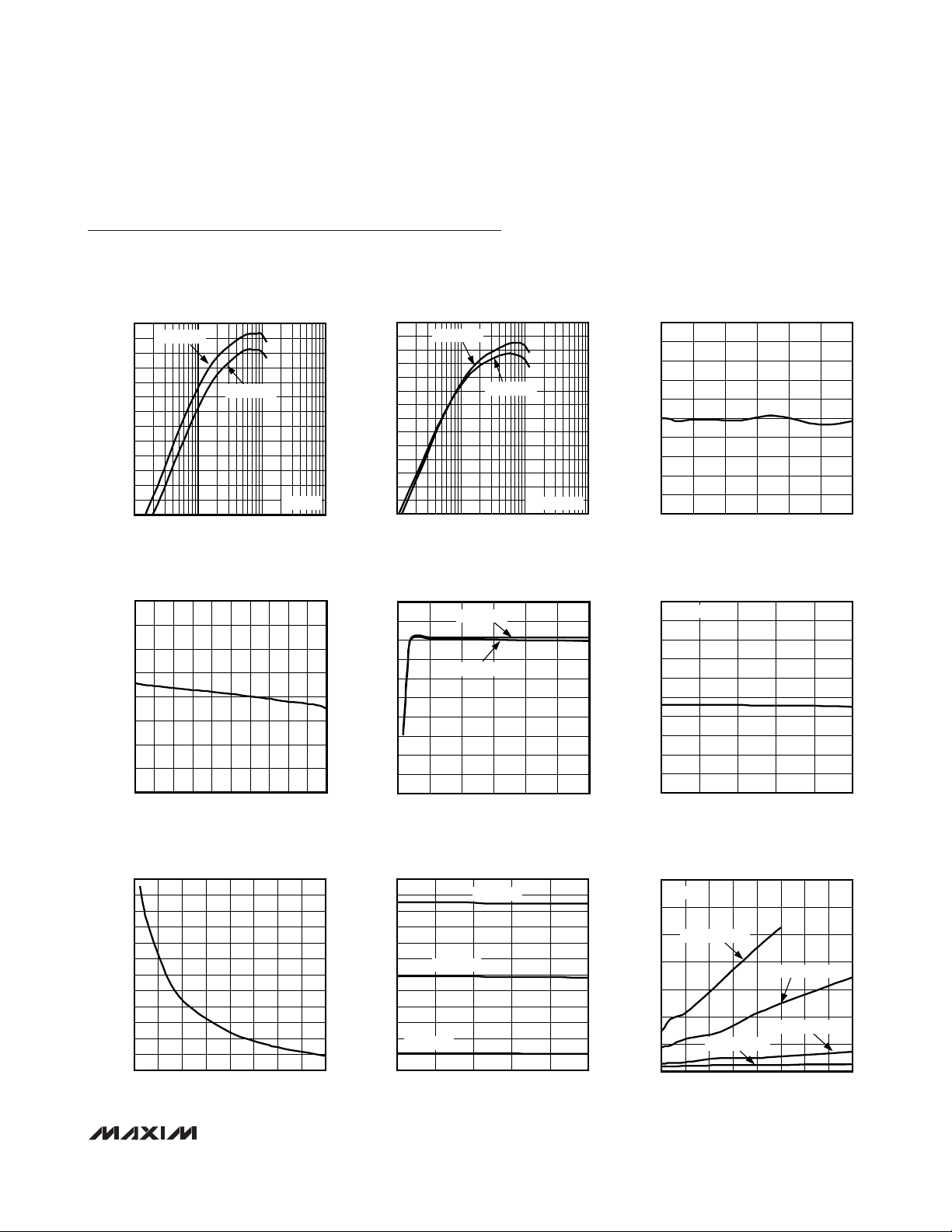
Typical Operating Characteristics
(Supply = IN = 12V, unless otherwise noted. See
Typical Application Circuit
of Figure 6.)
EFFICIENCY
vs. LOAD CURRENT
95
V
90
85
80
75
70
65
60
55
EFFICIENCY (%)
50
45
40
35
30
0.1 100
= 3.3V
OUT1
LOAD CURRENT (A)
MAX15023 toc01
V
= 1.2V
OUT1
VIN = 12V
101
VCC VOLTAGE
vs. LOAD CURRENT
5.40
5.35
5.30
5.25
5.20
5.15
SUPPLY VOLTAGE (V)
5.10
5.05
5.00
0 150
LOAD CURRENT (mA)
MAX15023 toc04
13512015 30 45 75 9060 105
EFFICIENCY
vs. LOAD CURRENT
100
95
90
85
80
75
70
65
60
EFFICIENCY (%)
55
50
45
40
35
30
V
= 3.3V
OUT1
0.1 100
LOAD CURRENT (A)
VCC VOLTAGE
vs. IN VOLTAGE
5.50
5.35
5.20
5.05
4.90
4.75
VOLTAGE (V)
4.60
CC
V
4.45
4.30
4.15
4.00
428
I
= 5mA
LOAD
I
= 50mA
LOAD
IN VOLTAGE (V)
V
OUT1
= 1.2V
VIN = VCC = 5V
101
OUTPUT VOLTAGE CHANGE
101.0
100.8
MAX15023 toc02
100.6
100.4
100.2
100.0
99.8
99.6
OUTPUT VOLTAGE CHANGE (%)
99.4
99.2
99.0
012
5.50
I
= 5mA
LOAD
5.45
5.40
MAX15023 toc05
5.35
5.30
5.25
5.20
SUPPLY VOLTAGE (V)
5.15
5.10
5.05
5.00
242016128
-40 85
vs. LOAD CURRENT
MAX15023 toc03
OUT1
108642
LOAD CURRENT (A)
VCC VOLTAGE
vs. TEMPERATURE
MAX15023 toc06
303510-15
TEMPERATURE (°C)
SWITCHING FREQUENCY
vs. R
1300
1200
1100
1000
900
800
700
600
500
400
SWITCHING FREQUENCY (kHz)
300
200
100
10 90
T
RT (kΩ)
SWITCHING FREQUENCY
vs. TEMPERATURE
800
750
700
MAX15023 toc07
650
600
550
500
450
400
350
SWITCHING FREQUENCY (kHz)
300
RT = 66.5kΩ
250
200
807050 6030 4020
-40 85
RT = 22.1kΩ
RT = 33.2kΩ
603510-15
TEMPERATURE (°C)
MAX15023 toc08
210
VIN = 12V
180
150
120
90
CURRENT (mA)
IN
I
60
30
0
200 1000
IIN CURRENT
vs. SWITCHING FREQUENCY
CDL = C
= 10nF
DH
CDL = C
DH
CDL = C
CDL = C
= 0nF
DH
SWITCHING FREQUENCY (kHz)
= 4.7nF
= 1nF
DH
MAX15023 toc09
900800700600500400300
Page 6
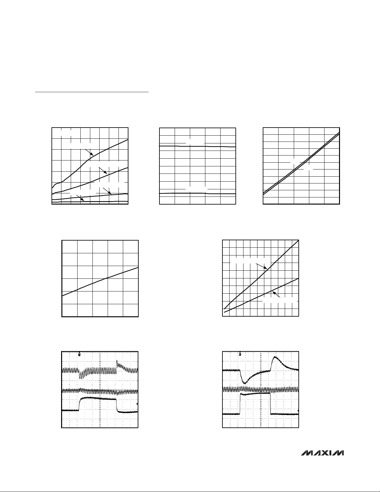
MAX15023
Wide 4.5V to 28V Input, Dual-Output
Synchronous Buck Controller
6 _______________________________________________________________________________________
Typical Operating Characteristics (continued)
(Supply = IN = 12V, unless otherwise noted. See
Typical Application Circuit
of Figure 6.)
I
IN
+ I
VCC
CURRENT
vs. SWITCHING FREQUENCY
MAX15023 toc10
SWITCHING FREQUENCY (kHz)
I
IN
+ I
VCC
CURRENT (mA)
900800700600500400300
30
60
90
120
150
180
210
0
200 1000
VIN = V
CC
= 5V
C
DL_
= C
DH_
= 10nF
C
DL_
= C
DH_
= 4.7nF
C
DL_
= C
DH_
= 1nF
CDL = C
DH
= 0nF
EN_ TURN-ON AND TURN-OFF THRESHOLD
vs. TEMPERATURE
MAX15023 toc11
TEMPERATURE (°C)
EN_ TURN-ON AND TURN-OFF THRESHOLDS
603510-15
1.025
1.050
1.075
1.100
1.125
1.150
1.175
1.200
1.225
1.250
1.000
-40 85
EN_ RISING
EN_ FALLING
LIM_ CURRENT
vs. TEMPERATURE
MAX15023 toc12
TEMPERATURE (°C)
LIM_ CURRENT (µA)
603510-15
40
42
44
46
48
50
52
54
56
58
60
38
-40 85
I
LIM2
I
LIM1
SHUTDOWN CURRENT
vs. TEMPERATURE
MAX15023 toc13
TEMPERATURE (°C)
SHUTDOWN CURRENT (µA)
603510-15
205
210
215
220
225
230
200
-40 85
CURRENT-LIMIT THRESHOLD
vs. R
LIM
MAX15023 toc14
R
LIM
(kΩ)
CURRENT-LIMIT THRESHOLD (mV)
555040 4515 20 25 30 3510
30
60
90
120
150
180
210
240
270
300
0
560
SOURCE CURRENT LIMIT
SINK CURRENT LIMIT
LOAD TRANSIENT ON OUT1
MAX15023 toc15
10µs/div
V
OUT1
(AC-COUPLED)
100mV/div
V
OUT2
(AC-COUPLED)
50mV/div
I
OUT1
5A/div
LOAD TRANSIENT ON OUT2
MAX15023 toc16
10µs/div
V
OUT2
(AC-COUPLED)
200mV/div
V
OUT1
(AC-COUPLED)
100mV/div
I
OUT2
2A/div
Page 7
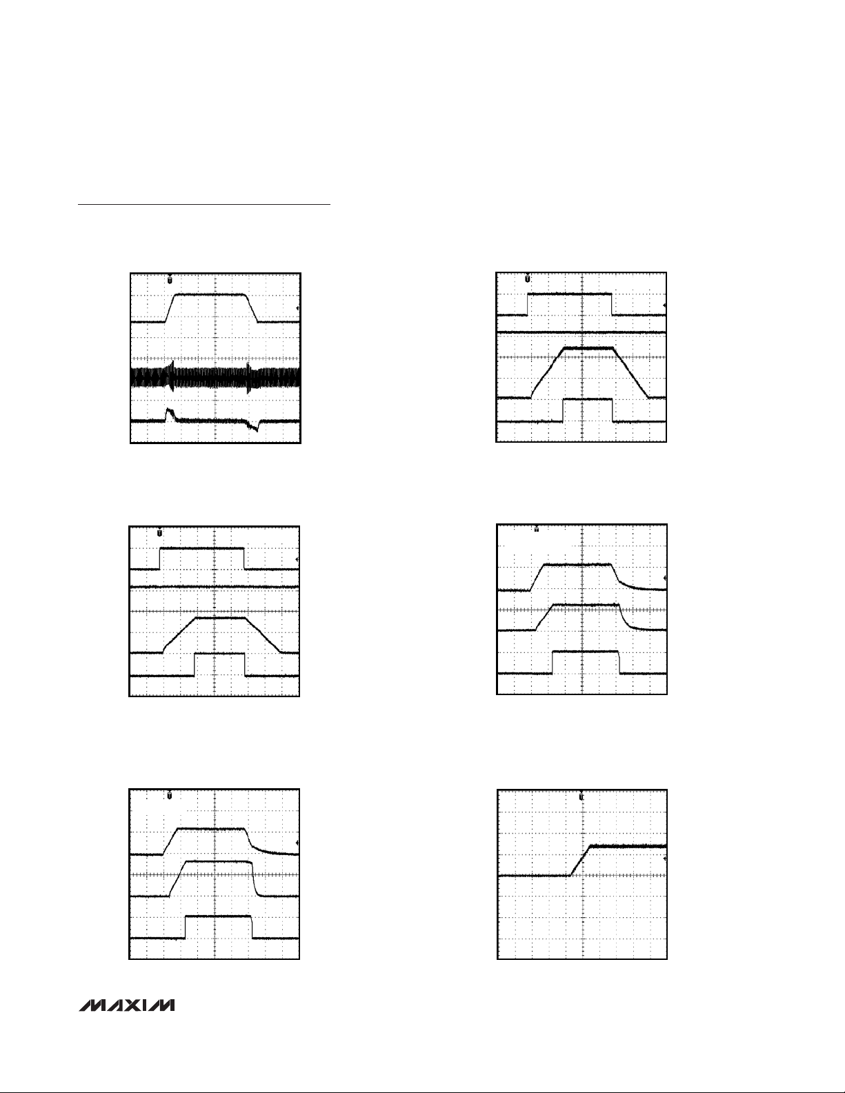
MAX15023
Wide 4.5V to 28V Input, Dual-Output
Synchronous Buck Controller
_______________________________________________________________________________________ 7
Typical Operating Characteristics (continued)
(Supply = IN = 12V, unless otherwise noted. See
Typical Application Circuit
of Figure 6.)
STARTUP AND DISABLE FROM EN
MAX15023 toc19
2ms/div
V
EN2
5V/div
V
IN
10V/div
V
OUT2
2V/div
V
PGOOD2
5V/div
I
OUT2
= 500mA
STARTUP AND TURN-OFF FROM IN
MAX15023 toc20
4ms/div
V
IN
10V/div
V
OUT1
1V/div
V
PGOOD1
5V/div
EN1 = EN2 = V
CC
I
OUT1
= 1.2A
STARTUP AND TURN-OFF FROM IN
MAX15023 toc21
4ms/div
V
IN
10V/div
V
OUT2
2V/div
V
PGOOD2
5V/div
I
OUT2
= 500mA
STARTUP INTO PREBIASED OUTPUT
(0.5V PREBIASED)
MAX15023 toc22
2ms/div
V
OUT1
500mV/div
0V
LINE-TRANSIENT RESPONSE
MAX15023 toc17
2ms/div
V
IN
5V/div
V
OUT1
(AC-COUPLED)
50mV/div
V
OUT2
(AC-COUPLED)
100mV/div
STARTUP AND DISABLE FROM EN
MAX15023 toc18
2ms/div
V
EN1
5V/div
V
IN
10V/div
V
OUT1
500mV/div
V
PGOOD1
5V/div
I
OUT1
= 1.2A
Page 8
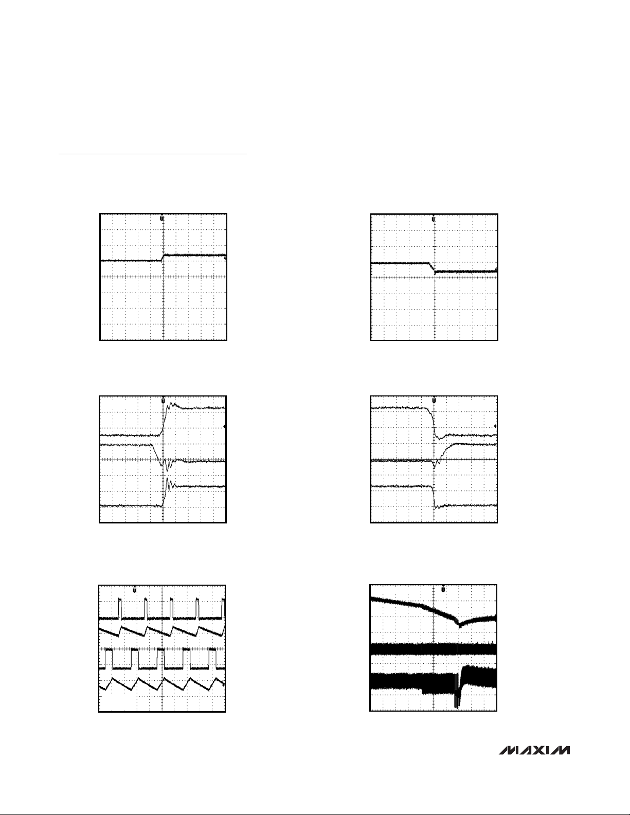
MAX15023
Wide 4.5V to 28V Input, Dual-Output
Synchronous Buck Controller
8 _______________________________________________________________________________________
Typical Operating Characteristics (continued)
(Supply = IN = 12V, unless otherwise noted. See
Typical Application Circuit
of Figure 6.)
STARTUP INTO PREBIASED OUTPUT
(1V PREBIASED)
MAX15023 toc23
2ms/div
V
OUT1
500mV/div
0V
STARTUP INTO PREBIASED OUTPUT
(1.5V PREBIASED)
MAX15023 toc24
2ms/div
V
OUT1
500mV/div
0V
DH_ AND DL_ DISOVERLAP
MAX15023 toc25
20ns/div
V
DH1
10V/div
V
DL1
5V/div
V
LX1
10V/div
I
OUT1
= 5A
DH_ AND DL_ DISOVERLAP
MAX15023 toc26
20ns/div
V
DH1
10V/div
V
DL1
5V/div
V
LX1
10V/div
I
OUT1
= 5A
OUT-OF-PHASE SWITCHING FORMS
MAX15023 toc27
1µs/div
V
LX1
10V/div
V
LX2
10V/div
I
LX1
5A/div
I
LX2
2A/div
I
OUT1
= 5A
I
OUT2
= 2.5A
SINK CURRENT-LIMIT WAVEFORMS
MAX15023 toc28
100µs/div
V
OUT1
200mV/div
V
LX1
20V/div
I
LX1
2A/div
1.5V PREBIASED
Page 9
MAX15023
Wide 4.5V to 28V Input, Dual-Output
Synchronous Buck Controller
_______________________________________________________________________________________ 9
Pin Description
PIN NAME FUNCTION
1 FB1
2 EN1
3 EN2
4 PGOOD1
5 DL1
6 PGND1
7 LX1
8 BST1
9 DH1
10 DH2
11 BST2
12 LX2
Feedback Input for Regulator 1. Connect FB1 to a resistive divider between Output 1 and SGND to adjust
the output voltage between 0.6V and (0.85 x input voltage (V)). See the Setting the Output Voltage section.
Active-High Enable Input for Regulator 1. When the voltage at EN1 exceeds 1.2V (typ), the controller begins
regulating OUT1. When the voltage falls below 1.05V (typ), the regulator is turned off. The EN1 input can be
used for power sequencing and as a secondary UVLO. Connect EN1 to V
Active-High Enable Input for Regulator 2. When the voltage at EN2 exceeds 1.2V (typ), the controller begins
regulating OUT2. When the voltage falls below 1.05V (typ), the regulator is turned off. The EN2 input can be
used for power sequencing and as a secondary UVLO. Connect EN2 to V
Power-Good Output (Open Drain) for Channel 1. To obtain a logic signal, pull up PGOOD1 with an external
resistor connected to a positive voltage below 28V.
Low-Side Gate-Driver Output for Regulator 1. DL1 swings from V
reaches the UVLO rising threshold voltage.
Low-Side Gate-Driver Supply Return (Regulator 1). Connect to the source of the low-side MOSFET of
Regulator 1.
External Inductor Connection for Regulator 1. Connect LX1 to the switched side of the inductor. LX1 serves
as the lower supply rail for the DH1 high-side gate driver and as sensing input of the synchronous
MOSFET’s V
Boost Flying-Capacitor Connection for Regulator 1. Connect a ceramic capacitor with a minimum value of
100nF between BST1 and LX1.
High-Side Gate-Driver Output for Regulator 1. DH1 swings from LX1 to BST1. DH1 is low before V
reaches the UVLO rising threshold voltage.
High-Side Gate-Driver Output for Regulator 2. DH2 swings from LX2 to BST2. DH2 is low before V
reaches the UVLO rising threshold voltage.
Boost Flying-Capacitor Connection for Regulator 2. Connect a ceramic capacitor with a minimum value of
100nF between BST2 and LX2.
External Inductor Connection for Regulator 2. Connect LX2 to the switched side of the inductor. LX2 serves
as the lower supply rail for the DH2 high-side gate driver and as sensing input of the synchronous
MOSFET’s V
drop (drain terminal).
DS
drop (drain terminal).
DS
for always-on applications.
CC
for always-on applications.
CC
to PGND1. DL1 is low before V
CC
CC
CC
CC
Page 10

MAX15023
Wide 4.5V to 28V Input, Dual-Output
Synchronous Buck Controller
10 ______________________________________________________________________________________
Pin Description (continued)
PIN NAME FUNCTION
13 PGND2
14 DL2
15 PGOOD2
16 V
CC
Low-Side Gate-Driver Supply Return (Regulator 2). Connect to the source of the low-side MOSFET of
Regulator 2.
Low-Side Gate-Driver Output for Regulator 2. DL2 swings from V
reaches the UVLO rising threshold voltage.
Power-Good Output (Open Drain) for Channel 2. To obtain a logic signal, pull up PGOOD2 with an external
resistor connected to a positive voltage below 28V.
Internal 5.2V Linear Regulator Output and the Device’s Core Supply. When using the internal regulator,
bypass V
operation, then a 2.2µF ceramic capacitor is adequate for decoupling (see the Typical Application Circuits).
to SGND with a 4.7µF minimum low-ESR ceramic capacitor. If VCC is connected to IN for 5V
CC
CC
to PGND2. DL2 is low before V
CC
17 FB2
18 COMP2 Compensation Pin for Regulator 2. See the Compensation section.
19 RT
20 SGND
21 IN
22 LIM2
23 LIM1
24 COMP1 Compensation Pin for Regulator 1. See the Compensation section.
—EP
Feedback Input for Regulator 2. Connect FB2 to a resistive divider between output 2 and SGND to adjust
the output voltage between 0.6V and (0.85 x input voltage (V)). See the Setting the Output Voltage section.
Oscillator-Timing Resistor Input. Connect a resistor from RT to SGND to set the oscillator frequency from
200kHz to 1MHz (see the Setting the Switching Frequency section).
Signal Ground. Connect SGND to the SGND plane. SGND also serves as sensing input of the synchronous
MOSFET’s V
Internal V
linear regulator (V
Current-Limit Adjustment for Regulator 2. Connect a resistor (R
current-limit threshold (V
Cycle-by-Cycle Low-Side Source Peak Current Limit section.
Current-Limit Adjustment for Regulator 1. Connect a resistor (R
current-limit threshold (V
Cycle-by-Cycle Low-Side Source Peak Current Limit section.
Exposed Paddle. Connect EP to a large copper plane at SGND potential to improve thermal dissipation. Do
not use as the main IC’s SGND ground connection.
drop (source terminals) for both channels.
DS
Regulator Input. Bypass IN to SGND with a 1µF minimum ceramic capacitor when the internal
CC
) is used. When operating in the 5V ±10% range, connect IN to VCC.
CC
) from 30mV (R
ITH2
) from 30mV (R
ITH1
= 6kΩ) to 300mV (R
LIM2
= 6kΩ) to 300mV (R
LIM1
LIM2
LIM1
) from LIM2 to SGND to adjust the
= 60kΩ). See the Setting the
LIM2
) from LIM1 to SGND to adjust the
= 60kΩ). See the Setting the
LIM1
Page 11

MAX15023
Wide 4.5V to 28V Input, Dual-Output
Synchronous Buck Controller
______________________________________________________________________________________ 11
Functional Diagram
COMP1
M
FB1
ENABLE1
g
DAC_VREF
SOFT-START/
VREF
DC-DC CONVERTER 1
HICCUP TIMEOUT
AND
STOP LOGIC
HICCUP LOGIC
HICCUP
PWM
PWM
COMPARATOR
RAMP
RAMP
GENERATOR
CK1
BST1
CK1
GATEP
BOOST
DRIVER
DH1
LX1
DL1
PGND1
FB1
PGOOD1
HIGH-
SIDE
DRIVER
CC
V
HICCUP
PWM
LOGIC
CONTROL
HICCUP
TIMEOUT
REF
V
LOW-SIDE DRIVER
LIM1/20
ENABLE1
SINK
COMPARATOR
CURRENT-LIMIT
PGOOD
COMPARATOR
REF
0.925 x V
LIM1/10
SOURCE
COMPARATOR
CURRENT-LIMIT
MAX15023
DC-DC CONVERTER 2
COMP2 BST2 DH2 PGND2
RT
CK2
VREF
CK1
OSCILLATOR
ENABLE1
CK2
ENABLE1 ENABLE2
COMPARATOR
VREF
EN1
ENABLE2
LIM2
VREF
ENABLE2
COMPARATOR
VREF
EN2
ENABLE
THERMAL
SHUTDOWN
LOGIC
BIAS
STARTUP
SGND
SGND LIM1
MAX15023 GEN
GENERATOR
LIM1
CC
IN
UVLO
VOLTAGE
INTERNAL
REGULATOR
VREF
BANDGAP
V
UVLO
VREF = 0.6V
CC
V
IN
REFERENCE
LIM
LIM2
CURRENT
PGOOD2 FB2 DL2 LX2
Page 12

MAX15023
Wide 4.5V to 28V Input, Dual-Output
Synchronous Buck Controller
12 ______________________________________________________________________________________
Detailed Description
The MAX15023 dual, synchronous, step-down controller operates from a 5.5V to 28V or 5V ±10% input
voltage range and generates two independent output
voltages. As long as the controller’s input bias voltage
is within the specified range, the input power bus can
also be lower than 4.5V and step-down conversion
from a 3.3V rail is also possible. Both output voltages
can be set from 0.6V to 85% of regulator’s input voltage. Each output can support loads of 12A or higher.
The switching sequence of the regulators is interleaved
with 180° out-of-phase operation, so that input voltage
ripple and total RMS input ripple current are reduced.
Enable inputs with precise turn-on/off threshold
(±4.2%) allow accurate external UVLO settings. Powergood (PGOOD) open-drain outputs can be used for
supply sequencing.
The MAX15023’s capability to provide low output voltages (down to 0.6V) and high output current (in excess
of 12A) makes it ideal for applications where a 5V or
12V bus is postregulated to deliver low voltages and
high currents, such as in set-top boxes.
The switching frequency is adjustable from 200kHz to
1MHz using an external resistor. The MAX15023’s
adaptive synchronous rectification eliminates the need
for external freewheeling Schottky diodes.
The MAX15023 utilizes voltage-mode control and external compensation. The device also utilizes cycle-bycycle low-side source peak current limit for overcurrent
protection, where the external low-side MOSFET’s onresistance is used as a current-sense element during
the inductor freewheeling time, eliminating the need for
a current-sense resistor. The current-limit threshold
voltage is resistor adjustable independently on each
regulator from 30mV to 300mV and is temperature
compensated, so that the effects of the MOSFET’s
R
DS(ON)
variation over temperature are reduced.
Hiccup-mode current limit reduces average current
and power dissipation during a prolonged short-circuit
condition.
The MAX15023 also features a proprietary adaptive
internal digital soft-start and allows prebias startup
without discharging the output. Adaptive digital softstart, by acting on the loop voltage reference, automatically prolongs the soft-start time, if the current-limit
threshold is reached during the soft-start sequence.
This increases the ability to smoothly bring up a large,
unknown amount of output capacitance. Also, since
soft-start is invoked during hiccup-mode short-circuit
protection, the same voltage reference rollback algorithm achieves good control of the peak inductor current during steady short-circuit or overload conditions.
An additional protection feature (cycle-by-cycle lowside sink peak current limit) prevents the regulators from
sinking excessive amount of current if the prebias voltage exceeds the programmed steady-state regulation
level, or if another voltage source is trying to force the
output above that. This way, the synchronous rectifier
MOSFET and the body diode of the high-side MOSFET
do not experience dangerous levels of current stress
while the regulator is sinking current from the output.
Thermal shutdown protects the MAX15023 from excessive power dissipation.
DC-DC PWM Controller
The MAX15023 step-down controller uses a PWM voltage-mode control scheme (see the
Functional
Diagram
) for each channel. Control loop compensation
is external for providing maximum flexibility in choosing
the operating frequency and output LC filter components. An internal transconductance error amplifier produces an integrated error voltage at COMP_ that helps
provide higher DC accuracy. The voltage at COMP_
sets the duty cycle using a PWM comparator and a
ramp generator. On the rising edge of its internal clock,
the high-side n-channel MOSFET of each regulator
turns on and remains on until either the appropriate
duty cycle or the maximum duty cycle is reached.
During the high-side MOSFET’s on-time, the inductor
current ramps up. During the second-half of the switching cycle, the high-side MOSFET turns off and the lowside n-channel MOSFET turns on. Now the inductor
releases the stored energy as its current ramps down,
providing current to the output. Under overload conditions, when the inductor current exceeds the selected
cycle-by-cycle low-side source peak current-limit
threshold (see the
Current-Limit Circuit (LIM_)
section),
the high-side MOSFET does not turn on at the subsequent clock rising edge and the low-side MOSFET
remains on to let the inductor current ramp down.
Interleaved Out-of-Phase Operation
The two independent regulators in the MAX15023 operate 180° out-of-phase to reduce input filtering requirements, reduce electromagnetic interference (EMI), and
improve efficiency. This effectively lowers component
cost and saves board space, making the MAX15023
ideal for cost-sensitive applications.
Page 13

MAX15023
The internal oscillator frequency is divided down to
obtain separated clock signals for each regulator. The
phase difference of the two clock signals is 180°, so that
the high-side MOSFETs turn on out-of-phase. The instantaneous input current peaks of both regulators no longer
overlap, resulting in reduced RMS ripple current and
input voltage ripple. As a result, this allows an input
capacitor with a lower ripple-current rating to be used or
allows the use of fewer or less expensive capacitors, as
well as reduces EMI filtering and shielding requirements.
Internal 5.2V Linear Regulator
The MAX15023’s internal functions and MOSFET drivers
are designed to operate from a 5V ±10% supply voltage. If the available supply voltage exceeds 5.5V, a
5.2V internal low-dropout linear regulator is used to
power internal functions and the MOSFET drivers at
V
CC
. If an external 5V ±10% supply voltage is available,
then IN and V
CC
can be tied to the 5V supply. The maxi-
mum regulator input voltage (V
IN
) is 28V. The regulator’s
input (IN) must be bypassed to SGND with a 1µF
ceramic capacitor when the regulator is used. Bypass
the regulator’s output (VCC) with a 4.7µF ceramic
capacitor to SGND. The V
CC
dropout voltage is typically
70mV, so when V
IN
is greater than 5.5V, VCCis typically
5.2V. The MAX15023 also employs a UVLO circuit that
disables both regulators when V
CC
falls below 3.8V
(typ). The 430mV UVLO hysteresis prevents chattering
on power-up/power-down.
The internal VCClinear regulator can source up to
100mA to supply the IC, power the low-side gate drivers, recharge the external boost capacitors, and supply small external loads. The current available for
external loads depends on the current consumed for
the MOSFET gate drive.
For example, when switched at 600kHz, a single
MOSFET with 18nC total gate charge (at V
GS
= 5V)
requires 18nC x 600kHz ≅ 11mA. Since four MOSFETs
are driven and 6mA (max) is used by the internal control functions, the current available for external loads is:
(100 – (4 x 11) – 6)mA ≅ 50mA
MOSFET Gate Drivers (DH_, DL_)
The DH_ and DL_ drivers are optimized for driving
large size n-channel power MOSFETs. Under normal
operating conditions and after startup, the DL_ low-side
drive waveform is always the complement of the DH_
high-side drive waveform (with controlled dead time to
prevent cross-conduction or shoot-through). On each
channel, an adaptive dead-time circuit monitors the DH
and DL outputs and prevents the opposite-side
MOSFET from turning on until the other MOSFET is fully
off. Thus, the circuit allows the high-side driver to turn
on only when the DL_ gate driver has been turned off.
Similarly, it prevents the low-side (DL_) from turning on
until the DH_ gate driver has been turned off.
The adaptive driver dead time allows operation without
shoot-through with a wide range of MOSFETs, minimizing
delays, and maintaining efficiency. There must be a lowresistance, low-inductance path from the DL_ and DH_
drivers to the MOSFET gates for the adaptive dead-time
circuits to work properly. Otherwise, because of the stray
impedance in the gate discharge path, the sense circuitry could interpret the MOSFET gates as off while the V
GS
of the MOSFET is still high. To minimize stray impedance, use very short, wide traces (50 mils to 100 mils
wide if the MOSFET is 1in from the driver).
Synchronous rectification reduces conduction losses in
the rectifier by replacing the normal low-side Schottky
catch diode with a low-resistance MOSFET switch. The
internal pulldown transistor that drives DL_ low is
robust, with a 0.75Ω (typ) on-resistance. This low onresistance helps prevent DL_ from being pulled up during the fast rise time of the LX_ node, due to capacitive
coupling from the drain to the gate of the low-side synchronous rectifier MOSFET.
High-Side Gate-Drive Supply (BST_)
and Internal Boost Switches
The high-side MOSFET is turned on by closing an internal switch between BST_ and DH_. This provides the
necessary gate-to-source voltage to turn on the high-side
MOSFET, an action that boosts the gate drive signal
above V
IN
. The boost capacitor connected between
BST_ and LX_ holds up the voltage across the floating
gate driver during the high-side MOSFET on-time.
The charge lost by the boost capacitor for delivering the
gate charge is refreshed when the high-side MOSFET is
turned off and LX_ node swings down to ground. When
the corresponding LX_ node is low, an internal high-voltage switch connected between V
CC
and BST_ recharges
the boost capacitor to the VCCvoltage. The need for
external boost diodes is negated. See the
Boost Flying-
Capacitor Selection
section in the
Design Procedure
section to choose the right size of the boost capacitor.
Enable Inputs (EN_),
Adaptive Soft-Start and Soft-Stop
The MAX15023 can be used to regulate two independent outputs. Each of the two outputs can be turned on
and off independently of one another by controlling the
enable input of each phase (EN1 and EN2).
A logic-high on each enable pin turns on the corresponding channel. Then, the soft-start sequence is initiated by step-wise increasing the reference voltage of
Wide 4.5V to 28V Input, Dual-Output
Synchronous Buck Controller
______________________________________________________________________________________ 13
Page 14

MAX15023
Wide 4.5V to 28V Input, Dual-Output
Synchronous Buck Controller
14 ______________________________________________________________________________________
the error amplifier. The duration of the soft-start ramp is
2048 switching cycles and the resolution is 1/64 of the
steady-state regulation voltage. This allows a smooth
increase of the output voltage. A logic-low on each EN_
initiates a soft-stop sequence by stepping down the reference voltage of the error amplifier. After the soft-stop
sequence is completed, the MOSFET drivers are both
turned off. See Figure 1 for more detail.
Connect EN1 and EN2 to VCCfor always-on operation.
Owing to their accurate turn-on and turn–off thresholds,
EN1 and EN2 can be used as a UVLO adjustment input
and for power sequencing together with the PGOOD_
outputs. (See the
Setting the Enable Input (EN_)
section).
The adaptive action in the soft-start becomes visible if
the cycle-by-cycle, low-side, source peak current limit
is reached during the soft-start ramping sequence. In
this case, the rate-of-rise of the internal reference is
decreased, so that the PWM controller tries to regulate
to the inductor current around its limit value, rather than
the output voltage. The soft-start time can be prolonged
up to 4096 clock cycles (twice the normal soft-start
duration). This implementation allows the soft-start time
to be automatically adapted to the time necessary to
keep the LX current below the limit while charging the
output capacitor.
Since soft-start is invoked by the hiccup-mode shortcircuit protection, also see the
Hiccup Mode
Overcurrent Protection
section for additional details.
Power-Good Outputs (PGOOD_)
The MAX15023 includes two power-good comparators
to monitor the regulators’ output voltages and detect
the power-good threshold, fixed at 92.5% of the nominal FB voltage. The PGOOD_ outputs are open-drain
and should be pulled up with an external resistor to the
supply voltage of the logic input they drive. This voltage
should not exceed 28V. They can sink up to 2mA of
current while low.
Figure 1. MAX15023 Detailed Power-On/-Off Sequencing
UVLO
V
EN_
CC
CD
B
E
F
G
HIA
V
OUT_
2048 CLK
CYCLES
V
is higher than the UVLO threshold. EN_ is low.
CC
EN is pulled high. DH_ and DL_ start switching.
Normal operation.
drops below UVLO.
V
CC
V
goes above UVLO threshold. DH_ and DL_
CC
start switching. Normal operation.
EN_ is pulled low. V
EN_ is pulled high. DH_ and DL_ start switching.
Normal operation.
V
drops below UVLO.
CC
enters soft-stop.
OUT_
DAC_VREF_
DH_
DL_
SYMBOL DEFINITION
UVLO
V
CC
EN_
V
OUT_
DAC_VREF_
DH_
DL_
A
Undervoltage threshold value is provided in
the Electrical Characteristics table.
Internal 5.2V linear regulator output.
Active-high enable input.
Regulator output voltage.
Regulator internal soft-start and soft-stop signal.
Regulator high-side gate-driver output.
Regulator low-side gate-driver output.
V
rising while below the UVLO threshold.
CC
EN_ is low.
2048 CLK
CYCLES
SYMBOL DEFINITION
B
C
D
E
F
G
H
I
Page 15

MAX15023
Each PGOOD_ goes high (high impedance) when the
corresponding regulator output increases above 92.5%
of its nominal regulated voltage. Each PGOOD_ goes
low when the corresponding regulator output voltage
drops typically below 89.5% of its nominal regulated
voltage. PGOOD_ can be used as power-on-reset or
power sequencing for the two regulators.
PGOOD_ asserts low during the hiccup timeout period.
Startup into a Prebiased Output
When the controller starts into a prebiased output, the
DH_/DL_ complementary switching sequence is inhibited until the PWM comparator commands its first PWM
pulse. Until then, DH_ and DL_ are kept off so that the
converter does not sink current from the output. The
first PWM pulse occurs when the ramping reference
voltage increases above the FB_ voltage or the internal
soft-start time is over.
Current-Limit Circuit (LIM_)
The current-limit circuit employs a cycle-by-cycle lowside source peak and sink current-sensing algorithm
that uses the on-resistance of the low-side MOSFET as
a current-sensing element, so that costly sense resistors are not required. The current-limit circuit is also
temperature compensated to track the MOSFET’s onresistance variation over temperature. The current limit
is adjustable on each channel with an external resistor
at LIM_ (see the
Typical Application Circuits
), and
accommodates MOSFETs with a wide range of onresistance characteristics (see the
Design Procedure
section). The adjustment range is from 30mV to 300mV
for the cycle-by-cycle, low-side, source peak current
limit, corresponding to resistor values of 6kΩ to 60kΩ.
The cycle-by-cycle, low-side, sink peak current-limit
threshold across the low-side MOSFET is precisely 1/10
the voltage seen at LIM_, while the cycle-by-cycle, lowside, sink peak current-limit threshold is 1/20 the voltage seen at LIM_.
The MAX15023 uses SGND to sense the voltage of the
source terminals of the low-side MOSFETs for both
channels, and LX_ to sense the drain voltage of each
low-side MOSFET. Carefully observe the
PCB Layout
Guidelines
section to ensure that noise and systematic
errors do not corrupt the current-sense signals seen by
LX_ and SGND on each channel.
Cycle-by-cycle, low-side, source peak current limit acts
when the inductor current flows in the normal direction,
and the drain (LX_) is more negative than source
(sensed by SGND) during the low-side MOSFET ontime. If the magnitude of current-sense signal exceeds
the cycle-by-cycle, low-side, source peak current-limit
threshold during the low-side MOSFET on-time, the
controller does not initiate a new PWM cycle and lets
the inductor current decay in the next cycle. Since
cycle-by-cycle, low-side, source peak current sensing
is employed, the actual peak current is greater than the
current-limit threshold by an amount equal to the inductor ripple current. Therefore, the exact current-limit
characteristic and maximum load capability are functions of the low-side MOSFET’s on-resistance, currentlimit threshold, inductor value, and input voltage.
Cycle-by-cycle, low-side, sink peak current limit is also
implemented by monitoring the voltage drop across the
low-side MOSFET, but with opposite polarity (drain
more positive than source). If this drop exceeds 1/20
the voltage at the corresponding LIM_ pin at any time
during the low-side MOSFET on-time, the low-side
MOSFET is turned off and the inductor current flows
from the output through the high-side MOSFET back. If
the cycle-by-cycle, low-side, sink peak current limit is
activated, the DH_ and DL_ switching sequence is no
longer complementary.
Hiccup Mode Overcurrent Protection
Hiccup mode overcurrent protection reduces power
dissipation during prolonged short-circuit or deep overload conditions.
After the soft-start sequence has been completed, on
each switching cycle where the cycle-by-cycle, low-side,
source peak current-limit threshold is reached, a 3-bit
counter is incremented. The counter is decremented on
each switching cycle where the threshold is not reached,
and stopped at zero (000).
If the cycle-by-cycle, low-side, source peak currentlimit condition persists, the counter fills up reaching 111
(= 7 events). Then, the controller stops both DL_ and
DH_ drivers and waits for 7936 switching cycles (hiccup timeout delay). After this delay, the controller initiates a new soft-start sequence.
If cycle-by-cycle, low-side, source peak current-limit
events occur during the soft-start time, turn-on cycles are
still skipped to control the inductor current, but the fill-up
of the 3-bit counter does not terminate the soft-start
sequence. Rather, the soft-start ramp is slowed down or
rolled back based on the cycle-by-cycle, low-side, source
peak current-limit events occurrences, so that the PWM
controller tries to regulate the inductor current around its
limit value, rather than the output voltage.
This proprietary technique prevents the duty cycle from
saturating, and limits the on-time and thus, the peak
inductor current is reached every time the high-side
MOSFET is turned on.
Wide 4.5V to 28V Input, Dual-Output
Synchronous Buck Controller
______________________________________________________________________________________ 15
Page 16

MAX15023
Wide 4.5V to 28V Input, Dual-Output
Synchronous Buck Controller
16 ______________________________________________________________________________________
In case of a nonideal short circuit applied at the output,
the output voltage equals the output impedance times the
limited inductor current during this phase. After reaching
the maximum allowable limit of the soft-start duration
(twice the normal soft-start time), the controller remains off
for 7936 clock cycles before trying to soft-start again.
Undervoltage Lockout
The MAX15023 has an internal undervoltage lockout
(UVLO) circuit to monitor the voltage on VCC. The
UVLO circuit prevents the MAX15023 from operating if
the voltages for the MOSFET drivers or for the internal
control functions are too low. The VCCfalling threshold
is 3.8V (typ), with 430mV hysteresis to prevent chattering on the rising/falling edge of the supply voltage.
Before VCCreaches UVLO rising threshold voltage,
DL_ and DH_ stay low to inhibit switching.
Thermal-Overload Protection
Thermal-overload protection limits total power dissipation
in the MAX15023. When the device’s die-junction temperature exceeds TJ= +150°C, an on-chip thermal sensor shuts down the device, forcing DL_ and DH_ low,
allowing the IC to cool. The thermal sensor turns the
device on again after the junction temperature cools by
20°C. During thermal shutdown, the regulators shut
down, and soft-start is reset. Thermal-overload protection
can be triggered by power dissipation in the LDO regulator, by excessive driving losses, or by both. Therefore,
carefully evaluate the total power dissipation (see the
Power Dissipation
section) to avoid unwanted triggering
of the thermal-overload protection in normal operation.
Design Procedure
Effective Input Voltage Range
Although the MAX15023 controllers can operate from
input supplies up to 28V and regulate down to 0.6V, the
minimum voltage conversion ratio (V
OUT/VIN
) might be
limited by the minimum controllable on-time. For proper
fixed-frequency PWM operation, the voltage conversion
ratio should obey the following condition:
where t
ON(MIN)
is 100ns (max) and fSWis the switching
frequency in Hertz. If the desired voltage conversion
does not meet the above condition, then pulse skipping
occurs to decrease the effective duty cycle. To avoid
this, decrease the switching frequency or lower the
input voltage VIN.
The maximum voltage conversion ratio is limited by the
maximum duty cycle (D
max
):
where V
DROP1
is the sum of the parasitic voltage drops
in the inductor discharge path, including synchronous
rectifier, inductor, and PCB resistances. V
DROP2
is the
sum of the resistances in the charging path, including
high-side switch, inductor, and PCB resistances. In
practice, the above condition should be met with adequate margin for good load-transient response.
Setting the Enable Input (EN_)
Each controller has an enable input referenced to an
analog voltage (1.2V). When the voltage exceeds 1.2V,
the regulator is enabled. To set a specific turn-on
threshold that can act as a secondary UVLO, a resistive
divider circuit can be used (see Figure 2)
Select R2(EN_ to SGND resistor) to a value lower than
200kΩ. Calculate R1(V
MON
to EN_ resistor) with the fol-
lowing equation:
where V
EN_H_
= 1.2V (typical).
EN_ off-time duration must be longer than 4096/fSWto
ensure proper soft-start operation, where fSWis in hertz.
Figure 2. Adjustable Enable Voltage
V
OUT
V
IN
<
D
D V (1 D ) V
max DROP2 max DROP1
−
max
×+ ×
−
V
IN
RR
12
⎡
⎢
⎢
⎣
⎛
⎜
⎝
V
MON
V
EN H
__
⎤
⎞
⎥
1=
−
⎟
⎥
⎠
⎦
V
OUT
tf
>×
N
I
ON(MIN) SW
V
EN_
MA15023
V
MON
R
1
R
2
Page 17

MAX15023
Setting the Output Voltage
Set the MAX15023 output voltage on each channel by
connecting a resistive divider from the output to FB_ to
SGND (Figure 3). Select R2(FB_ to SGND resistor) less
than or equal to 16kΩ. Calculate R1(OUT_ to FB_ resistor) with the following equation:
where V
FB_
= 0.6V (typ) (see the
Electrical Characteristics
table) and V
OUT_
can range from 0.6V to (0.85 x VIN).
Resistor R1also plays a role in the design of the Type
III compensation network. If a Type III compensation
network is used, make sure to review the values of R
1
and R2according to the
Type III Compensation
Network (See Figure 5)
section.
Setting the Switching Frequency
The switching frequency, fSW, for each channel is set
by a resistor (R
T
) connected from RT to SGND. The
relationship between f
SW
and RTis:
where f
SW
is in kHz, RT is in kΩ, and 24806 is in
1/farad. For example, a 600kHz switching frequency is
set with RT= 27.05kΩ. Higher frequencies allow
designs with lower inductor values and less output
capacitance. Consequently, peak currents and I2R
losses are lower at higher switching frequencies, but
core losses, gate-charge currents, and switching losses increase.
Inductor Selection
Three key inductor parameters must be specified for
operation with the MAX15023: inductance value (L),
inductor saturation current (I
SAT
), and DC resistance
(RDC). To select inductance value, the ratio of inductor
peak-to-peak AC current to DC average current (LIR)
must be selected first. A good compromise between
size and loss is a 30% peak-to-peak ripple current to
average-current ratio (LIR = 0.3). The switching frequency, input voltage, output voltage, and selected LIR
then determine the inductor value as follows:
where V
IN
, V
OUT
, and I
OUT
are typical values (so that
efficiency is optimum for typical conditions). The
switching frequency is set by R
T
(see the
Setting the
Switching Frequency
section). The exact inductor value
is not critical and can be adjusted in order to make
trade-offs among size, cost, efficiency, and transient
response requirements. Lower inductor values minimize
size and cost, but also improve transient response and
reduce efficiency due to higher peak currents. On the
other hand, higher inductance increases efficiency by
reducing the RMS current, but requires more output
capacitance to meet load-transient specifications.
Find a low-loss inductor having the lowest possible DC
resistance that fits in the allotted dimensions. The
inductor’s saturation rating (I
SAT
) must be high enough
to ensure that saturation can occur only above the maximum current-limit value, given the tolerance of the lowside MOSFET’s on-resistance and of the LIM_ reference
current (I
LIM
). On the other hand, these tolerances
should not prevent the converter from delivering the
rated load current (I
LOAD(MAX)
). Combining these con-
ditions, the inductor saturation current (I
SAT
) should be
such that:
where R
DS(ON,MAX)
and R
DS(ON,TYP)
are the maximum
and typical on-resistance of the low-side MOSFET. For
a given inductor type and value, choose the LIR corresponding to the worst-case inductor tolerance.
For LIR = 0.4, and a +25% on the low-side MOSFET’s
R
DS(ON,MAX)
, the inductor saturation current should be
about 50% greater than the converter’s maximum load
current. A variety of inductors from different manufacturers can be chosen to meet this requirement (for
example, Coilcraft MSS1278 series).
Figure 3. Adjustable Output Voltage
Wide 4.5V to 28V Input, Dual-Output
Synchronous Buck Controller
______________________________________________________________________________________ 17
⎡
⎛
V
OUT
RR
⎢
12
⎜
⎢
⎝
⎣
V
FB
⎤
⎞
_
⎥
1=
−
⎟
⎥
⎠
_
⎦
R
T
24806
=
()
f
SW
1 0663
.
OUT_
R
1
FB_
R
MA15023
2
VVV
OUT IN OUT
L
=
V f I LIR
IN SW OUT
R
I1I
SAT
DS(ON,MAX)
>×+
R
DS(ON,TYP)
−()
LIR
⎛
⎜
⎝
⎞
⎟
⎠
2
×
LOAD(MAX)
Page 18

MAX15023
Wide 4.5V to 28V Input, Dual-Output
Synchronous Buck Controller
18 ______________________________________________________________________________________
Setting the Cycle-by-Cycle, Low-Side,
Source Peak Current Limit
The minimum current-limit threshold must be high
enough to support the maximum expected load current
with the worst-case low-side MOSFET on-resistance
value since the low-side MOSFET’s on-resistance is
used as the current-sense element. The inductor’s
cycle-by-cycle, low-side, source peak current occurs at
I
LOAD(MAX)
minus half the ripple current. The ripple current is maximum when the inductor value is at the lower
limit of its specified tolerance. The minimum value of
the current-limit threshold voltage (V
ITH
) should be
greater than the voltage on the low-side MOSFET during the ripple-current valley:
where R
DS(ON)
is the on-resistance of the low-side
MOSFET in ohms. Use the maximum value for R
DS(ON)
from the low-side MOSFET’s data sheet.
To adjust the current-limit threshold, connect a resistor
(R
LIM_
) from LIM_ to SGND. The relationship between
the current-limit threshold (V
ITH_
) and R
LIM_
is:
where R
LIM_
is in kΩ and V
ITH_
is in mV.
An R
LIM_
resistance range of 6kΩ to 60kΩ corresponds
to a current-limit threshold of 30mV to 300mV. When
adjusting the current limit, use 1% tolerance resistors to
minimize errors in the current-limit threshold setting.
Input Capacitor
The input filter capacitor reduces peak currents drawn
from the power source and reduces noise and voltage
ripple on the input caused by the circuit’s switching.
The two converters of the MAX15023 run 180° out-ofphase, thereby, effectively doubling the switching frequency at the input and lowering the input RMS current.
The input ripple waveform would be unsymmetrical due
to the difference in load current and duty cycle between
converter 1 and converter 2. In fact, the worst-case input
RMS current occurs when only one controller is operating. The converter delivering the highest output power
(V
OUT
x I
OUT
) must be used in the formulas below:
The input capacitor RMS current requirement (I
RMS
) is
defined by the following equation:
I
RMS
has a maximum value when the input voltage
equals twice the output voltage (VIN= 2V
OUT
), so
I
RMS(MAX)
= I
LOAD(MAX)
/2.
Choose an input capacitor that exhibits less than +10°C
temperature rise at the RMS input current for optimal
long-term reliability.
The input voltage ripple is composed of ∆V
Q
(caused
by the capacitor discharge) and ∆V
ESR
(caused by the
ESR of the capacitor). Use low-ESR ceramic capacitors
with high ripple current capability at the input. Assume
the contribution from the ESR and capacitor discharge
are equal to 50%. Calculate the input capacitance and
ESR required for a specified input voltage ripple using
the following equations:
where:
and:
where:
All equations listed above are valid under the assumption that the input ports of both converters can be
merged in the physical layout, so that only one input
capacitor truly serves both converters. If this is not the
case, additional low-ESR, low-ESL ceramic capacitors
should be locally placed on each converter’s input port,
connected between the drain of the high-side MOSFET
and the source of the low-side MOSFET.
Output Capacitor
The key selection parameters for the output capacitor
are capacitance value, ESR, and voltage rating. These
parameters affect the overall stability, output ripple voltage, and transient response. The output ripple has two
components: variations in the charge stored in the output capacitor, and the voltage drop across the capacitor’s ESR caused by the current flowing into and out of
the capacitor:
LIR
VR I
>××
ITH DS ON MAX LOAD MAX
(, ) ( )
⎛
−
1
⎜
⎝
2
V
×10
R
=
LIM
50µ
ITH__
A
⎞
⎟
⎠
ESR
∆I
L
C
V
∆
ESR
=
IN
I
+
OUT
−()
VV V
IN OUT OUT
=
Vf L
××
IN SW
IDD
×
OUT
=
IN
∆
Vf
×
QSW
I
∆
L
2
×
−()1
V
OUT
D
=
V
IN
−
()
VVV
II
=
RMS LOAD MAX
()
OUT IN OUT
V
IN
∆∆∆VVV
RIPPLE ESR Q
≅+
Page 19

MAX15023
Wide 4.5V to 28V Input, Dual-Output
Synchronous Buck Controller
______________________________________________________________________________________ 19
The output voltage ripple as a consequence of the ESR
and the output capacitance is:
where ∆IL is the peak-to-peak inductor current ripple
(see the
Inductor Selection
section). These equations
are suitable for initial capacitor selection, but final values should be verified by testing in a prototype or evaluation circuit.
As a general rule, a smaller inductor ripple current
results in less output ripple voltage. The output capacitor must be also checked against load-transient
response requirements. The allowable deviation of the
output voltage during fast load transients also determines the output capacitance, its ESR, and its equivalent series inductance (ESL). The output capacitor
supplies the load current during a load step until the
controller responds with a greater duty cycle. The
response time (t
RESPONSE
) depends on the closed-
loop bandwidth of the converter (see the
Compensation
section). The resistive drop across the output capacitor’s ESR, the drop across the capacitor’s ESL (∆V
ESL
),
and the capacitor discharge causes a voltage droop
during the load step.
Use a combination of low-ESR tantalum/aluminum electrolytic or polymer and ceramic capacitors for better
transient load and voltage ripple performance. Nonleaded capacitors and capacitors in parallel help
reduce the ESL. Keep the maximum output voltage
deviation below the tolerable limits of the load. Use the
following equations to calculate the required ESR, ESL,
and capacitance value during a load step:
where I
STEP
is the load step, t
STEP
is the rise time of the
load step, t
RESPONSE
is the response time of the con-
troller, and fOis the closed-loop crossover frequency.
Compensation
Each channel of the MAX15023 provides an internal
transconductance amplifier with its inverting input and
its output available to the user for external frequency
compensation. The flexibility of external compensation
for each converter offers wide selection of output filtering components, especially the output capacitor. For
cost-sensitive applications, use low-ESR aluminum
electrolytic capacitors; for component-size sensitive
applications, use low-ESR tantalum, polymer, or ceramic capacitors at the output. The high switching frequency of the MAX15023 allows use of ceramic capacitors
at the output. Choose the small-signal components for
the error amplifier to achieve the desired closed-loop
bandwidth and phase margin.
To choose the appropriate compensation network type,
the power-supply poles and zeros, the zero crossover
frequency, and the type of the output capacitor must be
determined.
In a buck converter, the LC filter in the output stage
introduces a pair of complex poles at the following frequency:
The output capacitor and its ESR also introduce a zero
at:
The loop-gain crossover frequency (f
O
, where the loop
gain equals 1 (0dB)) should be set below 1/10 the
switching frequency:
Choosing a lower crossover frequency might also help
in reducing the effects of noise pickup into the feedback loop, such as jittery duty cycle.
In order to maintain a stable system, two stability criteria must be met:
1) The phase shift at the crossover frequency fO, must
be less than 180°. In other words, the phase margin
of the loop must be greater than zero.
2) The gain at the frequency where the phase shift is
-180° (gain margin) must be less than 1.
∆∆
V I ESR
=×
ESR L
∆
I
∆
V
=
Q
8
()
VV V
∆
IN OUT OUT
=
I
L
L
××
Cf
OUT SW
−
Vf L
IN SW
×
××
ESR
C
ESL
t
RESPONSE
V
∆
ESR
=
I
STEP
×
It
STEP RESPONSE
=
OUT
=
∆
Vt
∆
V
Q
×
ESL STEP
I
STEP
1
≅
×
3
f
O
f
=
PO
2π
f
=
ZO
2π
1
LC
××
OUT OUT
1
ESR C
××
f
≤
O
f
SW
10
OUT
Page 20

MAX15023
Wide 4.5V to 28V Input, Dual-Output
Synchronous Buck Controller
20 ______________________________________________________________________________________
It is recommended to have a phase margin around
+50° to +60° to maintain a robust loop stability and
well-behaved transient response.
If an electrolytic or large-ESR tantalum output capacitor
is used, the capacitor ESR zero fZOtypically occurs
between the LC poles and the crossover frequency f
O
(f
PO
< f
ZO
< fO). In this case, use a Type II (PI or pro-
portional-integral) compensation network.
If a ceramic or low-ESR tantalum output capacitor is
used, the capacitor ESR zero typically occurs above
the desired crossover frequency fO, that is f
PO
< fO <
f
ZO
. In this situation, choose a Type III (PID or propor-
tional-integral-derivative) compensation network.
Type II Compensation Network
(See Figure 4)
If fZOis lower than fOand close to fPO, the phase lead
of the capacitor ESR zero almost cancels the phase
loss of one of the complex poles of the LC filter around
the crossover frequency. Therefore, a Type II compensation network with a midband zero and a high-frequency pole can be used to stabilize the loop. In Figure
4, RFand CFintroduce a midband zero (fZ1). RFand
CCFin the Type II compensation network also provide a
high-frequency pole (fP1), which mitigates the effects of
the output high-frequency ripple.
To calculate the component values for Type II compensation network in Figure 4, follow the instruction below:
1) Calculate the gain of the modulator (Gain
MOD
)—
composed of the regulator’s pulse-width modulator,
LC filter, feedback divider, and associated circuitry
at crossover frequency:
where VINis the regulator’s input voltage, V
OSC
is the
amplitude of the ramp in the pulse-width modulator,
VFBis the FB_ input voltage set-point (0.6V typically,
see
Electrical Characteristics
table), and V
OUT
is the
desired output voltage.
The gain of the error amplifier (GainEA) in midband frequencies is:
where g
m
is the transconductance of the error amplifier.
The total loop gain as the product of the modulator gain
and the error amplifier gain at f
O
should equal 1. So:
Therefore:
Solving for RF:
2) Set a midband zero (fZ1) at 0.75 x f
PO
(to cancel
one of the LC poles):
Solving for CF:
3) Place a high-frequency pole at fP1= 0.5 x f
SW
(to
attenuate the ripple at the switching frequency, fSW)
and calculate CCFusing the following equation:
Figure 4. Type II Compensation Network
V
Gain
MOD
IN
=×
V
OSC O OUT
Gain g R
EA m F
ESR
××
2π
fLVV
()
×
FB
OUT
=×
Gain Gain
MOD EA
×=1
V
IN
×
V
OSC O OUT
ESR
××
()21π
fLVV
FB
×××=
gR
OUT
VfLV
OSC O OUT OUT
R
=
F
2π
×××
()
×××
V V g ESR
FB IN m
×
2
××
π
1
RC
FF
f
075=
=×
.
f
Z
C
=
F
2075π .
1
Rf
×× ×
FPO
C
=
CF
π
V
OUT
R
1
R
2
V
REF
1
Rf
××
FSW
g
m
1
−
C
F
R
F
C
F
mF
PO1
COMP
C
CF
Page 21

MAX15023
Type III Compensation Network
(See Figure 5)
If the output capacitor used is a low-ESR tantalum or
ceramic type, the ESR-induced zero frequency is usually above the targeted zero crossover frequency (f
O
). In
this case, Type III compensation is recommended.
Type III compensation provides three poles and two
zeros at the following frequencies:
Two midband zeros (fZ1and fZ2) cancel the pair of
complex poles introduced by the LC filter:
f
P1
= 0
fP1introduces a pole at zero frequency (integrator) for
nulling DC output voltage errors:
Depending on the location of the ESR zero (fZO), f
P2
can be used to cancel it, or to provide additional attenuation of the high-frequency output ripple:
fP3attenuates the high-frequency output ripple.
The locations of the zeros and poles should be such
that the phase margin peaks around fO.
Ensure that RF>>2/gm(1/gm(MIN) = 1/600µS = 1.67kΩ)
and the parallel resistance of R1, R2, and RIis greater
than 1/gm. Otherwise, a 180° phase shift is introduced
to the response and will make it unstable.
The following procedure is recommended:
1) With RF≥ 10kΩ, place the first zero (fZ1) at 0.5 x
f
PO
:
so:
2) The gain of the modulator (Gain
MOD
)—composed of
the regulator’s pulse-width modulator, LC filter,
feedback divider, and associated circuitry at
crossover frequency is:
The gain of the error amplifier (Gain
EA
) in midband fre-
quencies is:
The total loop gain as the product of the modulator gain
and the error amplifier gain at f
O
should be equal to 1.
So:
Therefore:
Solving for CI:
3) If f
PO
< fO < f
ZO
< fSW/2, the second pole (fP2)
should be used to cancel fZO. This way, the Bode
plot of the loop gain plot does not flatten out soon
after the 0dB crossover, and maintains its
-20dB/decade slope up to 1/2 the switching frequency. This is likely to occur if the output capacitor is a
low-ESR tantalum or polymer. Then set:
f
P2
= f
ZO
If a ceramic capacitor is used, then the capacitor ESR
zero, fZO, is likely to be located even above 1/2 the
switching frequency, that is, f
PO
< fO< fSW/2 < fZO. In
this case, the frequency of the second pole (fP2) should
be placed high enough in order not to significantly
erode the phase margin at the crossover frequency. For
example, it can be set at 5 x fO, so that its contribution
to phase loss at the crossover frequency, fO, is only
about 11°:
f
P2
= 5 x f
O
Once fP2is known, calculate RI:
Wide 4.5V to 28V Input, Dual-Output
Synchronous Buck Controller
______________________________________________________________________________________ 21
f
=
1
Z
f
=
2
Z
1
RC
2
××
π
FF
1
CRR
2
×× +
π ()
1
II
2=××π
1
RC
II
f
P
2
f
P
3
2=××
π
R
F
1
×
CC
FCF
+
CC
FCF
2
××
π
1
RC
FF
f
05=
=×
.
PO1
f
Z
C
=
F
205π .
1
Rf
×× ×
FPO
V
Gain
MOD
IN
=×
V
OSC
()π
×× ×
2
1
2
fL C
O OUT OUT
Gain f C R
= ×××2π
EA O I F
Gain Gain
×=1
MOD EA
V
V
OSC
IN
×
()
2
×× ×
1
2
fC L
O OUT OUT
ππ
× ××× =
21
fCR
OIF
2π
××× ×
()
×
VR
IN F
VfLC
OSC O OUT OUT
C
=
I
R
=
I
fC
××
2
π
PI
1
2
Page 22

MAX15023
Wide 4.5V to 28V Input, Dual-Output
Synchronous Buck Controller
22 ______________________________________________________________________________________
4) Place the second zero (fZ2) at 0.2 x fOor at fPO,
whichever is lower and calculate R1using the following equation:
5) Place the third pole (fP3) at half the switching frequency and calculate C
CF
:
6) Calculate R
2
as:
MOSFET Selection
The MAX15023’s step-down controller drives two external logic-level n-channel MOSFETs as the circuit switch
elements. The key selection parameters to choose
these MOSFETs include:
• On-resistance (R
DS(ON)
)
• Maximum drain-to-source voltage (V
DS(MAX)
)
• Minimum threshold voltage (V
TH(MIN)
)
• Total gate charge (Qg)
• Reverse transfer capacitance (C
RSS
)
• Power dissipation
All four n-channel MOSFETs must be a logic-level type
with guaranteed on-resistance specifications at VGS=
4.5V. For maximum efficiency, choose a high-side
MOSFET (NH_) that has conduction losses equal to the
switching losses at the typical input voltage. Ensure
that the conduction losses at minimum input voltage do
not exceed MOSFET package thermal limits, or violate
the overall thermal budget. Also, ensure that the conduction losses plus switching losses at the maximum
input voltage do not exceed package ratings or violate
the overall thermal budget. Ensure that the MAX15023
DL_ gate drivers can drive a low-side MOSFET (NL_).
In particular, check that the dV/dt caused by NH_ turning on does not pull up the NL_ gate through NL_’s
drain-to-gate capacitance. This is the most frequent
cause of cross-conduction problems.
Gate-charge losses are dissipated by the driver and do
not heat the MOSFET. Therefore, if the drive current is
taken from the internal LDO regulator, the power dissipation due to drive losses must be checked. All
MOSFETs must be selected so that their total gate
charge is low enough; therefore, VCCcan power all four
drivers without overheating the IC:
where Q
G_TOTAL
is the sum of the gate charges of all
four MOSFETs.
Power Dissipation
Device’s maximum power dissipation depends on the
thermal resistance from the die to the ambient environment and the ambient temperature. The thermal resistance depends on the device package, PCB copper
area, other thermal mass, and airflow.
The power dissipated into the package (PT) depends on
the supply configuration (see the
Typical Application
Circuits
). It can be calculated using the following equation:
PT= VINx I
IN
For the circuits of Figures 7 and 8:
PT = V
CC
x (I
IN
+ I
VCC
)
where VINand VCCare the voltages at the respective
pins, I
IN
is the current at the input of the internal LDO
(IINis practically zero for the circuits of Figures 7 and
8), I
VCC
is the current consumed by the internal core
and drivers when the internal regulator is unused for 5V
supply operation (IN = VCC). See the corresponding
Typical Operating Characteristics
for the typical curves
of IINand I
VCC
current consumption vs. operating fre-
quency at various load capacitance values.
Figure 5. Type III Compensation Network
R
1
fC
π
2=××
ZI
2
R
−
I1
C
=
CF
()
R
21
×× ××
=×
C
F
fRC
SW F F
V
FB
−
VV
OUT FB
−205 1π .
R
V
OUT
R
R
I
1
C
I
R
2
C
CF
C
F
R
F
g
m
V
REF
PVQ f
=× ×
DRIVE IN G TOTAL SW
_
COMP
Page 23

MAX15023
To estimate the temperature rise of the die, use the following equation:
TJ= TA+ (PTx θJA)
where θJAis the junction-to-ambient thermal resistance
of the package, PTis power dissipated in the device,
and TAis the ambient temperature. The θ
JA
is 36°C/W
for the 24-pin TQFN package on multilayer boards, with
the conditions specified by the respective JEDEC standards (JESD51-5, JESD51-7). If actual operating conditions significantly deviate from those described in the
JEDEC standards, then an accurate estimation of the
junction temperature requires a direct measurement of
the case temperature (TC). Then, the junction temperature can be calculated using the following equation:
TJ= TC+ (PTx θJC)
Use 3°C/W as θJCthermal resistance for the 24-pin
TQFN package. The case-to-ambient thermal resistance (θCA) is dependent on how well the heat is transferred from the PCB to the ambient. Therefore, solder
the exposed pad of the TQFN package to a large copper area to spread heat through the board surface,
minimizing the case-to-ambient thermal resistance. Use
large copper areas to keep the PCB temperature low.
Boost Flying-Capacitor Selection
The MAX15023 uses a bootstrap circuit to generate the
necessary gate-to-source voltage to turn on the highside MOSFET. The selected n-channel high-side MOSFET determines the appropriate boost capacitance
values (C
BST_
in
Typical Application Circuits
) according
to the following equation:
where Qg is the total gate charge of the high-side
MOSFET and ∆V
BST_
is the voltage variation allowed on
the high-side MOSFET driver after turn-on. Choose
∆V
BST_
such that the available gate drive voltage is not
significantly degraded (e.g., ∆V
BST_
= 100mV to
300mV) when determining C
BST_
. The boost flyingcapacitor should be a low-ESR ceramic capacitor. A
minimum value of 100nF is recommended.
Applications Information
PCB Layout Guidelines
Make the controller ground connections as follows: create a small analog ground plane near the IC or use a
dedicated internal plane. Connect this plane to SGND
and use this plane for the ground connection for the IN
bypass capacitor, compensation components, feedback dividers, RT resistor, and LIM_ resistors.
If possible, place all power components on the top side
of the board, and run the power stage currents (especially the one having large high-frequency components)
using traces or copper fills on the top side only, without
adding vias.
On the top side, lay out a large PGND copper area for
the output of channels 1 and 2, and connect the bottom
terminals of the high-frequency input capacitors, output
capacitors, and the source terminals of the low-side
MOSFETs to that area.
Then, make a star connection of the SGND plane to the
top copper PGND area with few vias in the vicinity of
the source terminal sensing. Do not connect PGND and
SGND anywhere else. Refer to the MAX15023
Evaluation Kit data sheet for guidance.
Keep the power traces and load connections short,
especially at the ground terminals. This practice is
essential for high efficiency and jitter-free operation. Use
thick copper PCBs (2oz vs. 1oz) to enhance efficiency.
Place the controller IC adjacent to the synchronous rectifier MOSFETs (NL _) and keep the connections for
LX_, PGND_, DH_, and DL_ short and wide. Use multiple small vias to route these signals from the top to the
bottom side. The gate current traces must be short and
wide, measuring 50 mils to 100 mils wide if the low-side
MOSFET is 1in from the controller IC. Connect each
PGND trace from the IC close to the source terminal of
the respective low-side MOSFET.
Route high-speed switching nodes (BST_, LX_, DH_,
and DL_) away from the sensitive analog areas (RT,
COMP_, LIM_, and FB_). Group all SGND-referred and
feedback components close to the IC. Keep the FB_
and compensation network nets as small as possible to
prevent noise pickup.
Wide 4.5V to 28V Input, Dual-Output
Synchronous Buck Controller
______________________________________________________________________________________ 23
C
BST
Qg
=
∆
V
BST__
Page 24

MAX15023
Wide 4.5V to 28V Input, Dual-Output
Synchronous Buck Controller
24 ______________________________________________________________________________________
Typical Application Circuits
Figure 6. Application Diagram (Operation from a Single-Supply Rail, VIN= 9V to 16V)
V
OUT1
12.1kΩ
16.2kΩ
12.1kΩ
EN1
200kΩ
PGOOD2
EN2
200kΩ
PGOOD1
V
IN
10µF
25V
V
OUT1
22µF
6.3V
10µF
25V
1500µF
2.5V
DL1
3300pF
22pF
V
CC
47kΩ
V
CC
47kΩ
Q1
FDS8880
C
BST1
0.8µH 3.3µH
2200pF
1.5Ω
0.22µF
30.1kΩ
2
EN1
15
PGOOD2
3
EN2
4
PGOOD1
9
DH1
8
BST1
Q3
FDS8880
1
24
FB1
LX1
7
Q2
FDS8880
VIN
9V TO 16V
23
21
IN
LIM1
COMP1
MAX15023
DL16PGND114DL2
5
1µF
20
SGND
PGND2
13
FDS6982AS-Q2
22
COMP2
FB2
V
DH2
BST2
LX2
12
LIM2
RT
CC
22.1kΩ
19
18
17
16
10
11
Q5
R
T
33kΩ
4.7µF
C
BST2
0.22µF
1.62kΩ
3300pF
20kΩ
Q4
FDS6982AS-Q1
2200pF
1.5Ω
390pF
33pF
45.3kΩ
10kΩ
22µF
6.3V
V
OUT2
V
CC
V
IN
10µF
25V
V
OUT2
22µF
22µF
6.3V
6.3V
Page 25

MAX15023
Typical Application Circuits (continued)
Figure 7. Application Diagram (Operation with VIN= VCC= 5V ±10%)
Wide 4.5V to 28V Input, Dual-Output
Synchronous Buck Controller
______________________________________________________________________________________ 25
V
OUT1
R
PU1
PGOOD1
V
4.5V TO 5.5V
C
IN1
L1
IN
R8
C5
R5
R7
EN1
EN2
V
IN
Q1
C8
C6
118COMP2
217FB2
316V
415PGOOD1 PGOOD2
514DL1 DL2
613PGND1 PGND2
R10 R9 R
R6
23
24
FB1
EN1
EN2
22
MAX15023
DH1 LIM2
BST1 LIM1
LX1 COMP1
9
8
7
C
BST1CBST2
21
DH2 IN
10
20
11
BST2 SGND
T
19
CC
LX2 RT
12
C5
C4
R4
C2
V
IN
R2
C3
R3
R1
R
PU2
PGOOD2
C
IN2
Q3
L2
V
OUT2
C
OUT1
Q2
Q4
C
OUT2
Page 26

MAX15023
Wide 4.5V to 28V Input, Dual-Output
Synchronous Buck Controller
26 ______________________________________________________________________________________
Typical Application Circuits (continued)
Figure 8. Application Diagram (Operation with Auxiliary 5V Supply and 3.3V Bus)
V
3.3V
IN
R8
C8
V
AUX
4.5V TO 5.5V
R
PU1
PGOOD1
C
IN1
L1
V
OUT1
C
OUT1
C5
R5
R7
EN1
EN2
Q1
Q2
C6
118COMP2
217FB2
316V
415PGOOD1 PGOOD2
514DL1 DL2
613PGND1 PGND2
R10 R9 R
R6
22
23
24
FB1
EN1
EN2
MAX15023
DH1 LIM2
BST1 LIM1
LX1 COMP1
9
8
7
C
BST1CBST2
20
21
DH2 IN
11
10
BST2 SGND
T
19
CC
LX2 RT
12
C5
C4
R4
C2
V
IN
3.3V
R2
C3
R3
R1
R
PU2
PGOOD2
C
IN2
Q3
L2
V
OUT2
Q4
C
OUT2
Page 27

MAX15023
Wide 4.5V to 28V Input, Dual-Output
Synchronous Buck Controller
Maxim cannot assume responsibility for use of any circuitry other than circuitry entirely embodied in a Maxim product. No circuit patent licenses are
implied. Maxim reserves the right to change the circuitry and specifications without notice at any time.
Maxim Integrated Products, 120 San Gabriel Drive, Sunnyvale, CA 94086 408-737-7600 ____________________
27
© 2008 Maxim Integrated Products is a registered trademark of Maxim Integrated Products, Inc.
Package Information
For the latest package outline information, go to
www.maxim-ic.com/packages
.
Chip Information
PROCESS: BiCMOS
PACKAGE TYPE PACKAGE CODE DOCUMENT NO.
24 TQFN-EP T2444-4
21-0139
 Loading...